DOI:10.32604/cmc.2022.026061
| Computers, Materials & Continua DOI:10.32604/cmc.2022.026061 | |
| Article |
A Compact Rhombus Shaped Antenna with Extended Stubs for Ultra-Wideband Applications
1Department of Electrical Engineering, IIC University of Technology, Phnom Penh, Cambodia
2Department of Computer Science, COMSATS University Islamabad, Abbottabad Campus, 22060, Pakistan
3Department of Electrical and Computer Engineering, COMSATS University Islamabad, Abbottabad Campus,22060, Pakistan
4School of Computer Science, SCS, Taylor’s University, Subang Jaya, 47500, Selangor, Malaysia
5Center for Smart Society 5.0, CSS5 Faculty of Innovation and Technology, Taylor’s University, Subang Jaya, 47500, Malaysia
6Department of Information Systems, College of Computer and Information Sciences, Jouf University, Al-Jouf, KSA
*Corresponding Author: NZ Jhanjhi. Email: noorzaman.jhanjhi@taylors.edu.my
Received: 14 December 2021; Accepted: 23 March 2022
Abstract: Ultra-wideband (UWB) is highly preferred for short distance communication. As a result of this significance, this project targets the design of a compact UWB antennas. This paper describes a printed UWB rhombus-shaped antenna with a partial ground plane. To achieve wideband response, two stubs and a notch are incorporated at both sides of the rhombus design and ground plane respectively. To excite the antenna, a simple microstrip feed line is employed. The suggested antenna is built on a 1.6 mm thick FR4 substrate. The proposed design is very compact with overall electrical size of 0.18λ × 0.25λ (14 × 18 mm2). The rhombus shaped antenna covers frequency ranging from 3.5 to 11 GHz with 7.5 GHz impedance bandwidth. The proposed design simulated and measured bandwidths are 83.33% and 80%, respectively. Radiation pattern in terms of E-field and H-field are discussed at 4, 5.5 and 10 GHz respectively. The proposed design has 65% radiation efficiency and 1.5 dBi peak gain. The proposed design is simulated in CST (Computer Simulation Technology) simulator and the simulated design is fabricated for the measured results. The simulated and measured findings are in close resemblance. The obtained results confirm the application of the proposed design for the ultra-wide band applications.
Keywords: Ultra-wideband; impedance bandwidth; radiation pattern; CST; electrical size
There is a significant improvement in the wireless technologies. Wireless devices are getting smarter not only in term of size but also in the provision of services. Antenna is an integral part of every wireless communication system. These days compact and wideband antennas are highly preferred. In 2002, the Federal Communications Commission (FCC) granted permission for ultra-wideband (UWB) uses in the 3.1–10.6 GHz spectrum [1]. It is important to note that UWB technology is very popular because of power-efficient wireless communication system. Moreover, for short-range communication UWB antennas are of great significance [2]. Low cost, high data rate, minimal power consumption, low complexity, are all advantages of the UWB system [3–5]. With the large scale commercialization of 5G infrastructure, efficient and highly compact wireless devices are required. For such wireless devices, compact UWB antennas that can cover the required frequency band with a good overall performance are highly demanded. Since long time UWB antennas are under consideration. Multiple antennas designs for UWB application have been reported in [6–15]. These published works highlight different aspects of the UWB antennas which include gain and efficiency enhancement, improvement in impedance matching and miniaturization. In [6] a heart shape, monopole antenna is presented with a band notch characteristic. The antenna operates over a bandwidth from 3 to 11 GHz. This design has an overall size of 50 × 50 mm2. This much size is relatively larger for the UWB applications, thus it minimizes the design significance. Similarly, in [7] an elliptical slot form rings monopole antenna with a bandwidth of 8 GHz is presented. The size of the design is 28 × 28 mm2. Although the design is compact, however the excitation by a separate circular disc makes it bulky and difficult to house in RF (Radio Frequency) systems. A bio-inspired leaf shape antenna with dimensions of314 × 121 mm2 is presented in [8]. The design is used for partial discharge monitoring in high-voltage insulation systems. The proposed UWB antenna has impedance bandwidth from 3 to 8 GHz. Additionally the design has truncated ground plane which helps in enhancing the operating bandwidth. A Vivaldi M- shaped antenna array is presented in [9]. The design has a high gain of 16 dBi. The design has an operating bandwidth of 5.6 GHz which is from 3.3 to 8 GHz. Although the design has a very good gain but it does not cover the complete UWB band. Moreover, the overall size of the design is too large which also reduces its usefulness. A compact UWB fractal antenna with stub loaded defected ground is presented in [10]. The design in this work has a very wide operating band and excellent performance. The design has an overall dimension of 30 × 24 × 1.6 mm3 and 17.53 GHz operating bandwidth. The gain of the proposed design is 6.48 dBi, however addition of multiple techniques to achieve the desired results make the design complex. The work in [16] describes two printed wide-slot antennas with E-shaped patches and slots. The design is fed via a coplanar waveguide (CPW) feedline and a microstrip line for broadband applications. The antenna has a large size of 85 × 85 mm2 (0.216λ × 0.216λ).This design has an operating bandwidth from 2.85 to 15.12 GHz. A microstrip printed monopole UWB antenna is proposed in [17]. The antenna is large, with the physical dimensions of 70 × 70 mm2 and an electrical length of (0.233λ × 0.233λ).This antenna’s bandwidth ranges from 1.73 to 9.36 GHz. The work in [18] proposes a monopole ultra wideband (UWB) antennas with half-wavelength symmetric circular slots etched on the radiating patch that operate in the UWB spectrum and have an electrical length of 0.408λ × 0.350λ.This antenna has a bandwidth from 3.5 to 12.5 GHz. The research in [19] demonstrates a spiral-shaped CPW-fed wideband (WB) slot antenna. The antenna is both complicated and large in size. The suggested antenna’s overall dimensions are 37 × 33 mm, with an electrical length of 0.291λ × 0.259λ × 0.012λ mm, however the dimensions as well as the electrical length are both relatively larger.
Several studies have been conducted on miniaturizing the size of UWB antenna. A miniaturized antenna for medical implantable application is discussed in [11]. The antenna's dimensions are as small as 9.2 × 11 mm2 and the bandwidth is approximately 1 GHz. Similarly, in [12] a slot monopole antenna with a resonating V shaped patch covers the UWB range. There is gain variations from 0.2 to 3.5 dBi. In [13] with size of 29 × 20 mm2, an open slot antenna with UWB response is presented. The design covers the operating band from 3.1–10.8 GHz with the value of gain between 4 to 5 dBi. In [14] another UWB antenna with an overall size of 34 × 33 mm2 is discussed. The recorded gain of the proposed design is 4.35 dBi. However, the measured gain for the whole operating band is inconsistent. Another z-shaped UWB antenna with a total area of 38 × 35 mm2 and a gain of 1.6–6.4 dBi is discussed in [15]. However, there the design has low impedance matching which minimizes its significance for real time applications.
From the above discussion, it is clear that a compact UWB antennas with good performance is highly preferred for multiple real time applications. Therefore, the design of simple, compact, and high performance UWB antennas needs thorough investigation. A printed simple UWB rhombus-shaped antenna is discussed in detail in this work. This antenna is designed on an FR4 substrate which low cost and easily available. The proposed antenna is very compact with the dimensions of 14 × 18 × 1.6 mm3. The antenna operates between 3.5 and 11 GHz, which cover UWB band. Moreover, the design has an acceptable values of gain and efficiency. The far field radiation pattern of the proposed design is stable at all the resonance frequencies.
The proposed design front and bottom views are given in Figs. 1a and 1b respectively. The detailed dimensions of the proposed design are given in Tab.1. The antenna is etched on a 1.6 mm thick FR4 substrate, with a loss tangent of 0.0009 and a dielectric constant of 4.3. The microstrip consists of copper with an electric conductivity of 5.8 × 10⁷ S/m. The proposed antenna has an overall size of 14 × 18 × 1.6
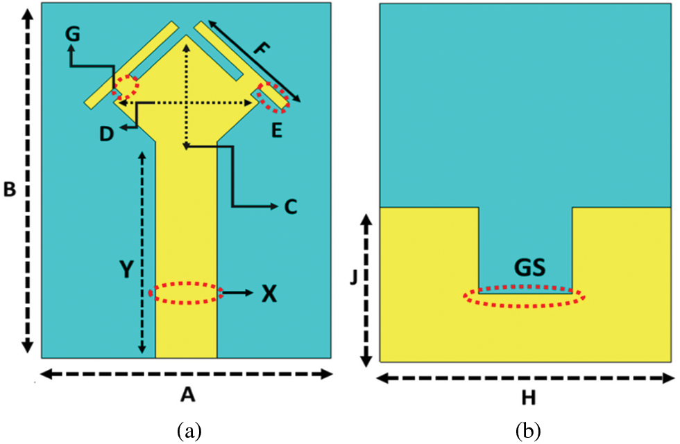
Figure 1: Proposed UWB antenna (a) Front View (b) Bottom View
The proposed design is simulated by using CST (Computer Simulation Technology) 2019 version. The proposed simple and compact design is finalized in three basic steps. First, a planar tetrahedron shaped radiating element is excited with a simple microstrip feedline on the upper side of the substrate. In the second step, the ground plane is truncated and a rectangular notch is introduced to it. In the third step, two stubs with two rectangular elements are attached with the tetrahedron shape to achieve the final design. Every design step brings certain improvement to the simulated results. Truncation of the ground plane with a rectangular notch enhances the operating bandwidth. At this stage, the targeted results do not satisfy the minimum requirement of the UWB design. To achieve the desired results, two stubs with two rectangular elements are added to the tetrahedron shaped radiator. The stubs change the current distribution on the radiator and this helps to widen the operating band with relatively good impedance matching.
Fig. 2 shows the design steps of the proposed antenna. The initial tetrahedron shaped antenna with truncated ground plane resonates at 8.6 GHz with a relatively narrow bandwidth and better impedance matching. With the introduction of the rectangular notch on the upper side of the truncated ground, the operating band is enhanced. However, it still needs improvement in the impedance matching. To improve impedance matching two stubs are introduced with tetrahedron shaped patch. This improve the impedance matching and at this stage, the design covers the whole UWB band.
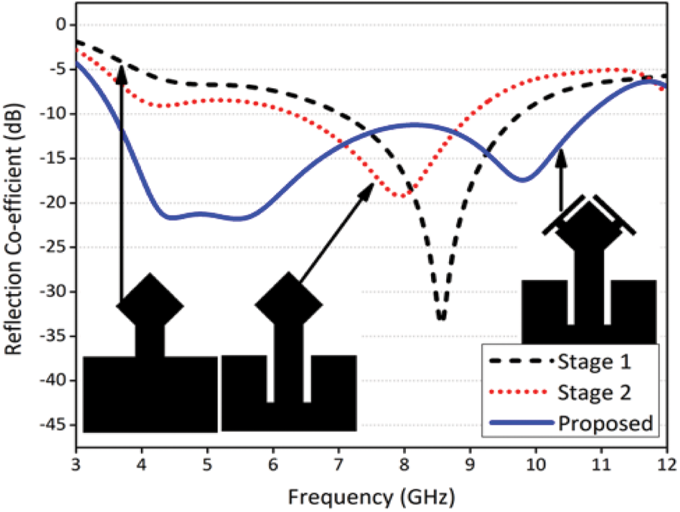
Figure 2: Stepwise design of the antenna and their corresponding reflection coefficient
3 Parametric Study of the proposed Antenna
In order to get the final design, the parametric study is performed on multiple parameters. This helps to observe the behavior of the different parameters and its impact on the simulated results. For this, the impact of the ground plane notch, length of the feedline and thickness of the attached stubs are analysed.
The first parameter for the parametric analysis is the ground plane notch. During the simulation, it is observed that the variation in the length of the ground plane has a minimum impact on the reflection coefficient. Therefore the parametric study on this parameter is not performed. It is also witnessed that the width of the ground plane notch changes the reflection coefficient. Fig. 3 shows that any increase or decrease in the ground plane notch will change the reflection coefficient. The width of the ground plane notch varies from 2 to 5 mm with the step size of 0.5 mm. From the simulated result of the parametric study of this parameter, it is found that with the increase in the width of the ground plane notch the impedance matching is reduced but the operating bandwidth is increased. With the value of 4.5 mm width for the ground plane notch, the target UWB band is achieved with an acceptable value of impedance matching.
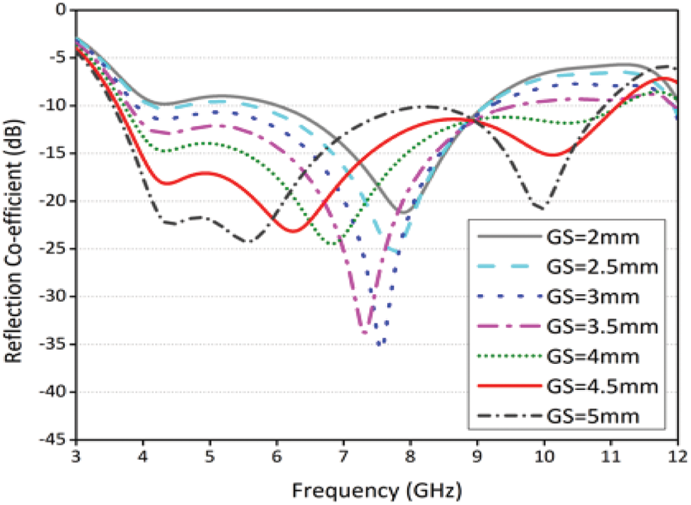
Figure 3: Parametric analysis of the ground plane slot impact on the reflection coefficient
Feedline length is another important parameter, which affects the reflection coefficient and impedance matching. As the width of the feedline is a predetermined fixed calculated value which depends on the dielectric constant of the substrate. Thus, the parametric study is performed on the length of the feed line. From the parametric study it is clear that, increasing the length of the feedline enhances the operating band width. As shown in Fig. 4, the length of the feed line is varied between 9.5 and 12 mm. The required UWB band with an acceptable value of the impedance matching is achieved at the length of 11.5 mm.
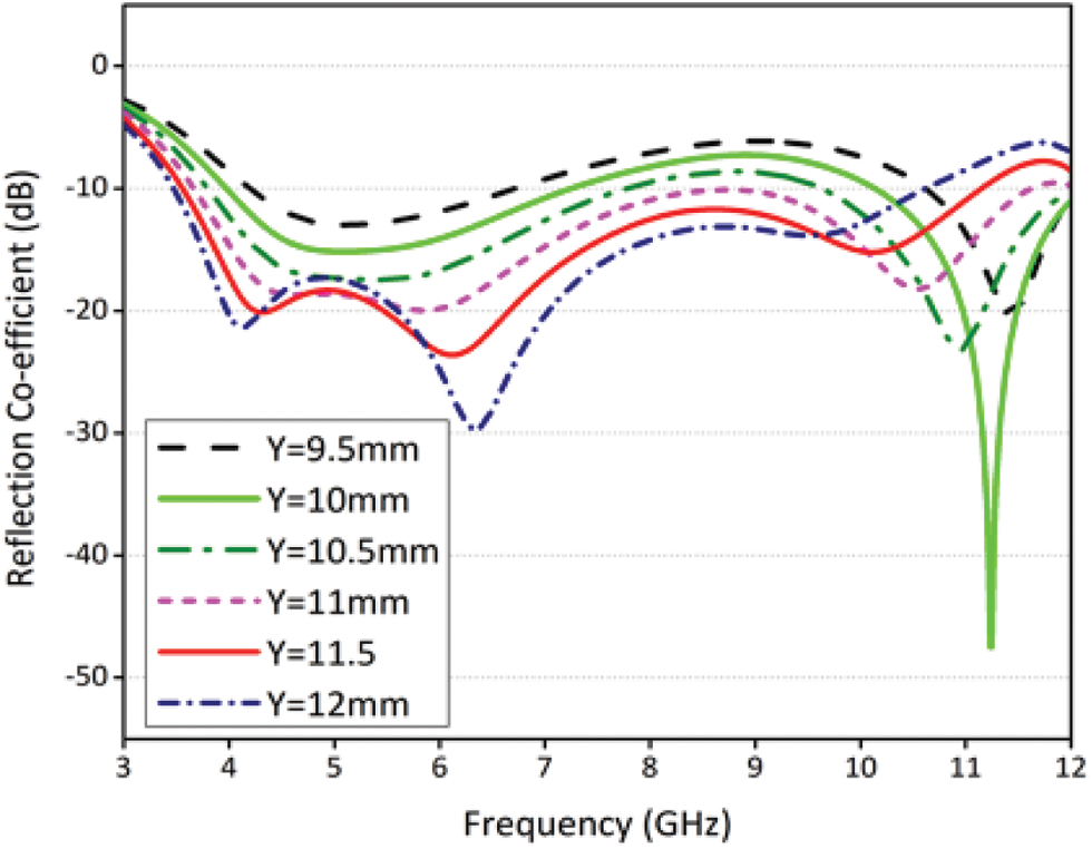
Figure 4: Parametric study of the impact of feedline length on the reflection coefficient
The last parametric study is performed on the attached rectangular elements with the stub thickness. The impact is understandable from the simulated values of the reflection coefficients as shown in Fig. 5. The stub thickness changes the current distribution on the stub as well as on the tetrahedron patch. As a result, there is a change in the simulated reflection coefficient and impedance matching. With the narrow thickness, the impedance matching has a good value but the UWB band is not achieved at this stage. At the 3.5 mm thickness, the design has UWB band with an acceptable value of the impedance matching.
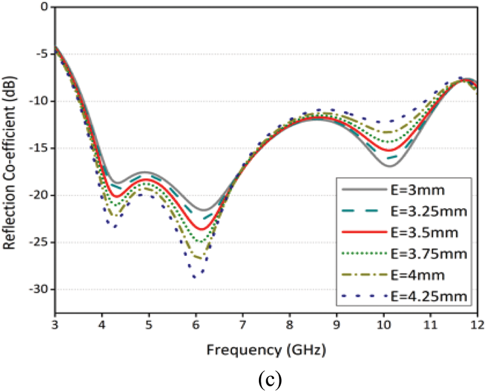
Figure 5: Parametric analysis on the impact of attached rectangular elements thickness on the reflection coefficients
4 Surface Current Distribution and Group Delay
The surface current distribution, Group Delay and E-field distribution are discussed in detail in this section. Figs. 6a–6c shows the current distribution at 4.5, 5.5 and 10 GHz respectively. For4.5 GHz the current is concentrated on the feedline and lower half of the Rhombus patch. For 5.5 GHz the maximum current activity in addition to feedline and lower half of the Rhombus is also witnessed on the ground plane. For 10 GHz the maximum current activity is noticed on the feedline, Rhombus patch and around the notch of the ground plane. Thus there is an increase in the current activity with the increase in the frequency.
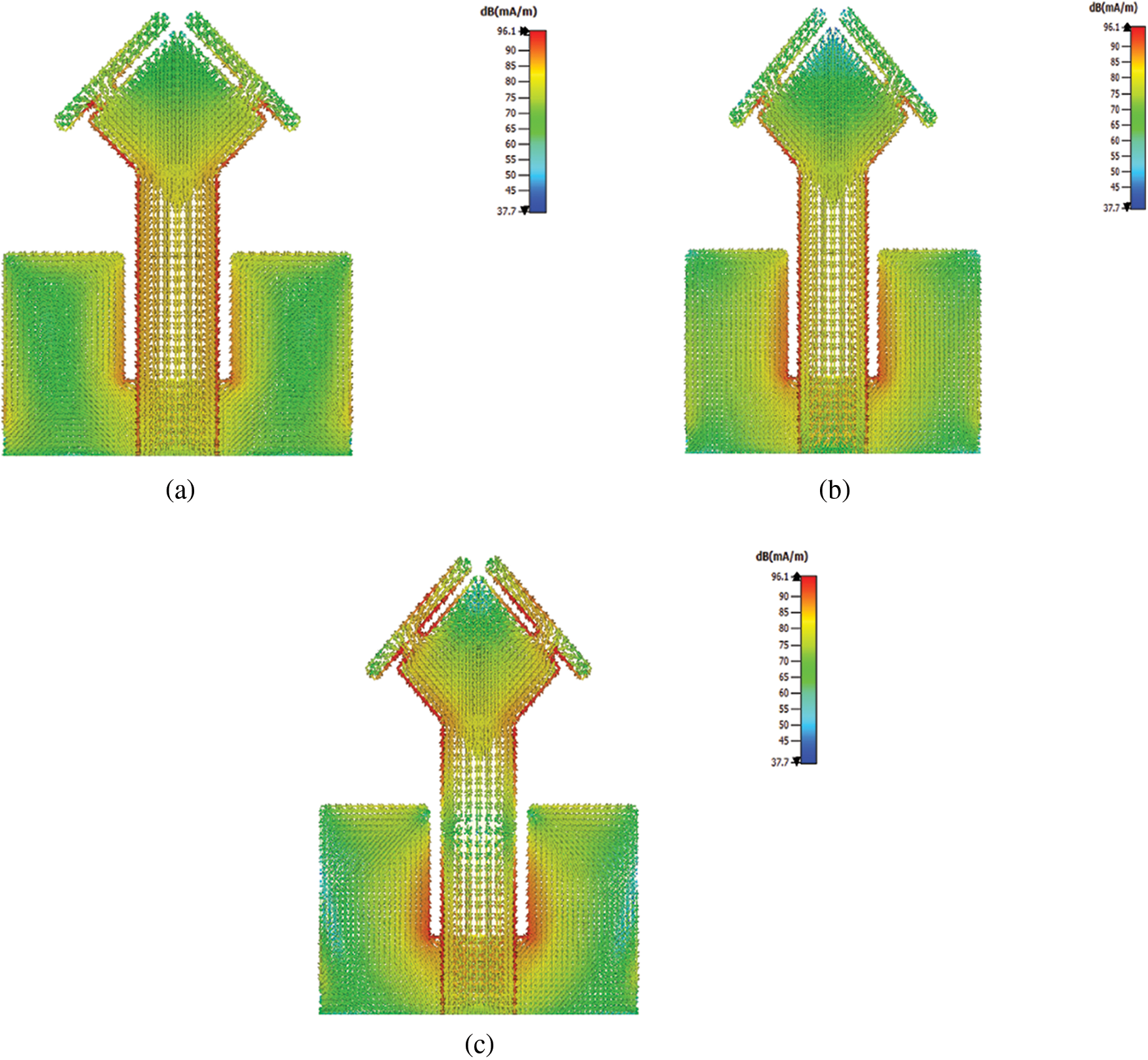
Figure 6: Current distribution at (a) 4 GHz, (b) 5.5 GHz and (c) 10 GHz
Fig. 7 shows the equivalent circuit model of the proposed UWB antenna. The upper patch, substrate and truncated ground plane with a rectangular notch are modelled as parallel resonance circuit. The equation used to determine these circuit elements are given below [16,20].
In the above equations the C, L, R are the capacitance, inductance and resistance of the equivalent modelled circuit.
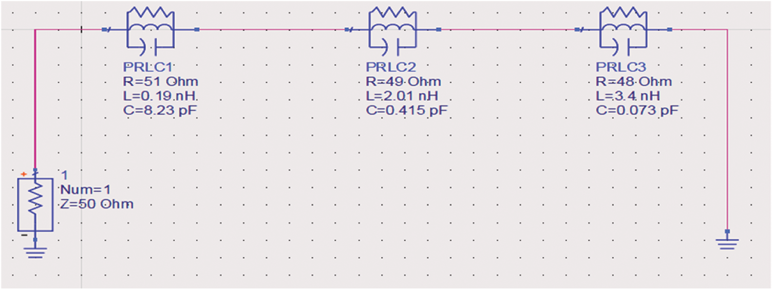
Figure 7: The equivalent circuit model of the proposed UWB antenna
The modes generated in the design at the three different resonance frequencies are given in the Fig. 8. For the three resonance frequencies, the design has three tank circuits. The proposed design is positioned in XY plane. As the design has a simple microstrip line feeding, thus transverse electric (TE) will be the dominant mode on the patch surface. Fig. 9 shows the dominant mode generated at the three different resonance frequencies is TE110. At 4.5 GHz, the E-fields have high concentration on the both stubs uniformly. At 5.5 GHz the E-field are concentrated on the lower edges of the stubs. At 10 GHz, the E-fields are distributed on the upper half of the stubs. Thus at the resonance frequencies, the E-field distribution changes which causes the generation of multiple resonance frequencies.
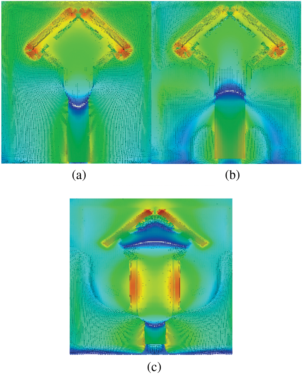
Figure 8: The E-field distribution on the patch at 4 GHz, 5.5 GHz and 10 GHz respectively
The group delay is an important parameter of the time domain analysis of the UWB antennas. It gives details of the delay in the signal while travelling from receiver to the transmitter [16]. In order to determine the group delay, the proposed design is positioned in two possible arrangements. Front to front and side by side are the two orientations. The distance between the two ends for both the arrangement is 35 mm. Fig. 9, shows that proposed design has a very small group delay for both the orientations which is considered a good value as compared to the published literature.
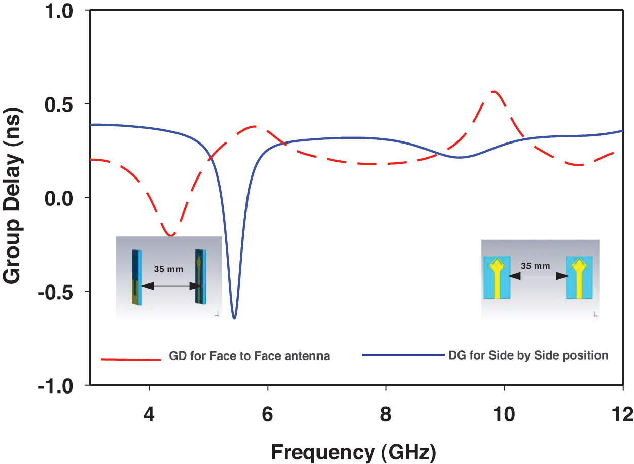
Figure 9: Group Delay of the design for fact to face and side by side arrangements
In this section, the simulated and measured results of the proposed design are discussed in detail. These include simulated and measure reflection coefficients, simulated and measured radiation patterns, 3D radiation pattern, simulated and measured gain and efficiency. Fig. 10, shows the simulated and measured reflection coefficients. From the Fig. 10, it is clear that in terms of the UWB coverage the simulated and measured values of the proposed design are in close agreement. However, due to fabrication errors, surrounding noise and power reflection from the port, the measured reflection coefficient has low impedance matching. In fact, a slight increase in the measured operating bandwidth at higher frequencies is noticed.
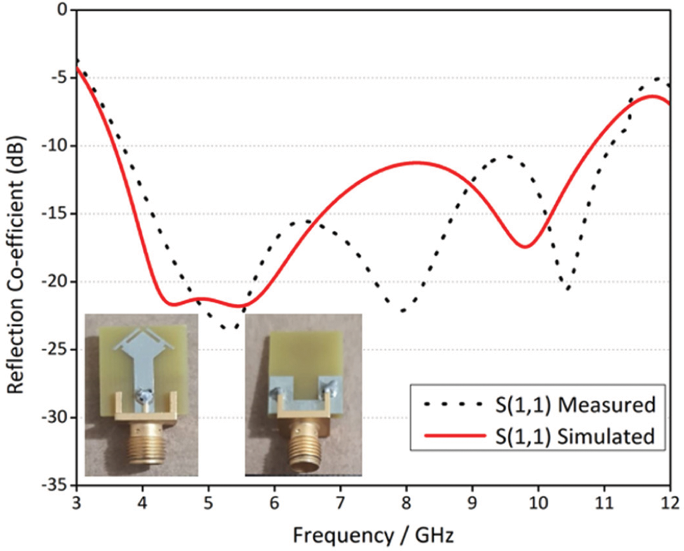
Figure 10: Simulated and measured reflection coefficients of the proposed design
Fig. 11 shows the detail of the simulated and measured efficiency and gain of the proposed design. The simulated peak efficiency of the proposed design is 66% while the measured peak efficiency of the proposed design is 68%. This slight increase is due to imperfect measurement environment and surrounding noise. Moreover, the simulated and measured efficiencies meet the requirements of the wireless applications. Fig. 11 also gives detail of the simulated and measured gain. The peak simulated and measure gain is 1.5 dBi. Due to the surrounding noise, there is a slight deviation in the measured values.
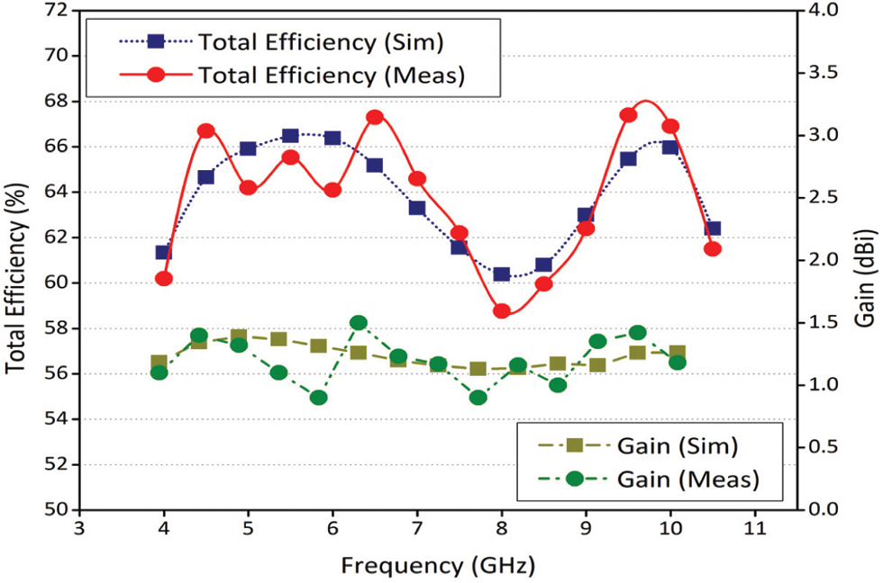
Figure 11: Simulated and measured efficiency and gain of the proposed antenna
Fig. 12 shows the far-field radiation pattern of the proposed design while Fig. 13 shows the 3D radiation pattern. The far-field radiation pattern is presented in terms of E-field and H-field. The E-field at 4 GHz has a broadside pattern. The simulated and measured E-field pattern are in close agreement in terms of beam width and main beam direction. The measured E-field pattern has a slightly decrease gain. Similarly, the H-field simulated and measured pattern are also in the same pattern with a minor degradation in terms of gain. The simulated and measured radiation pattern for 5.5 and 10 GHz are also in close agreement for the beam width and main lob direction. However, there is loss of 1 dBi for the measured radiation pattern.
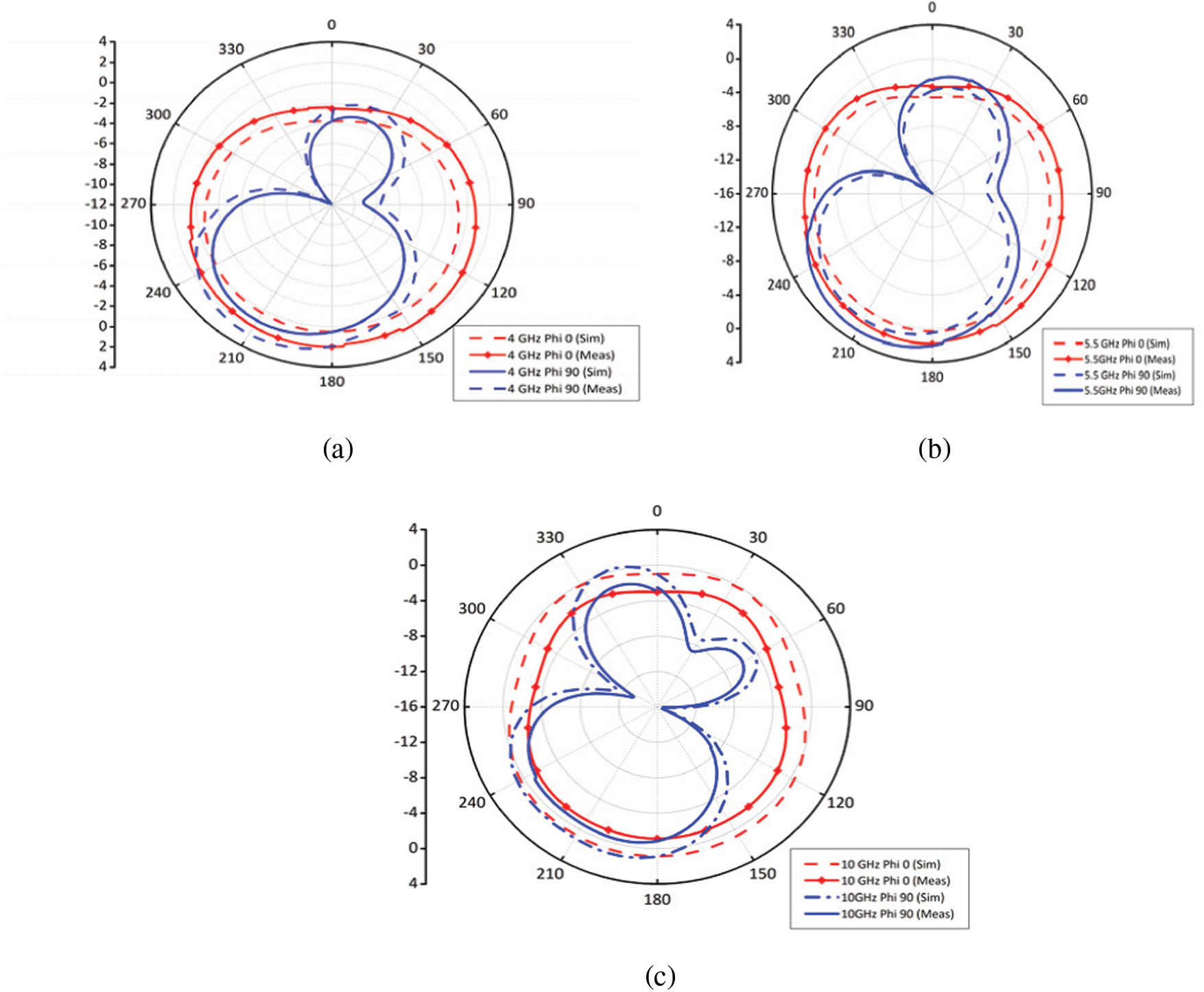
Figure 12: Radiation pattern in term of E-field and H-field at (a) 4 GHz, (b) 5.5 GHz and (d) 10 GHz respectively
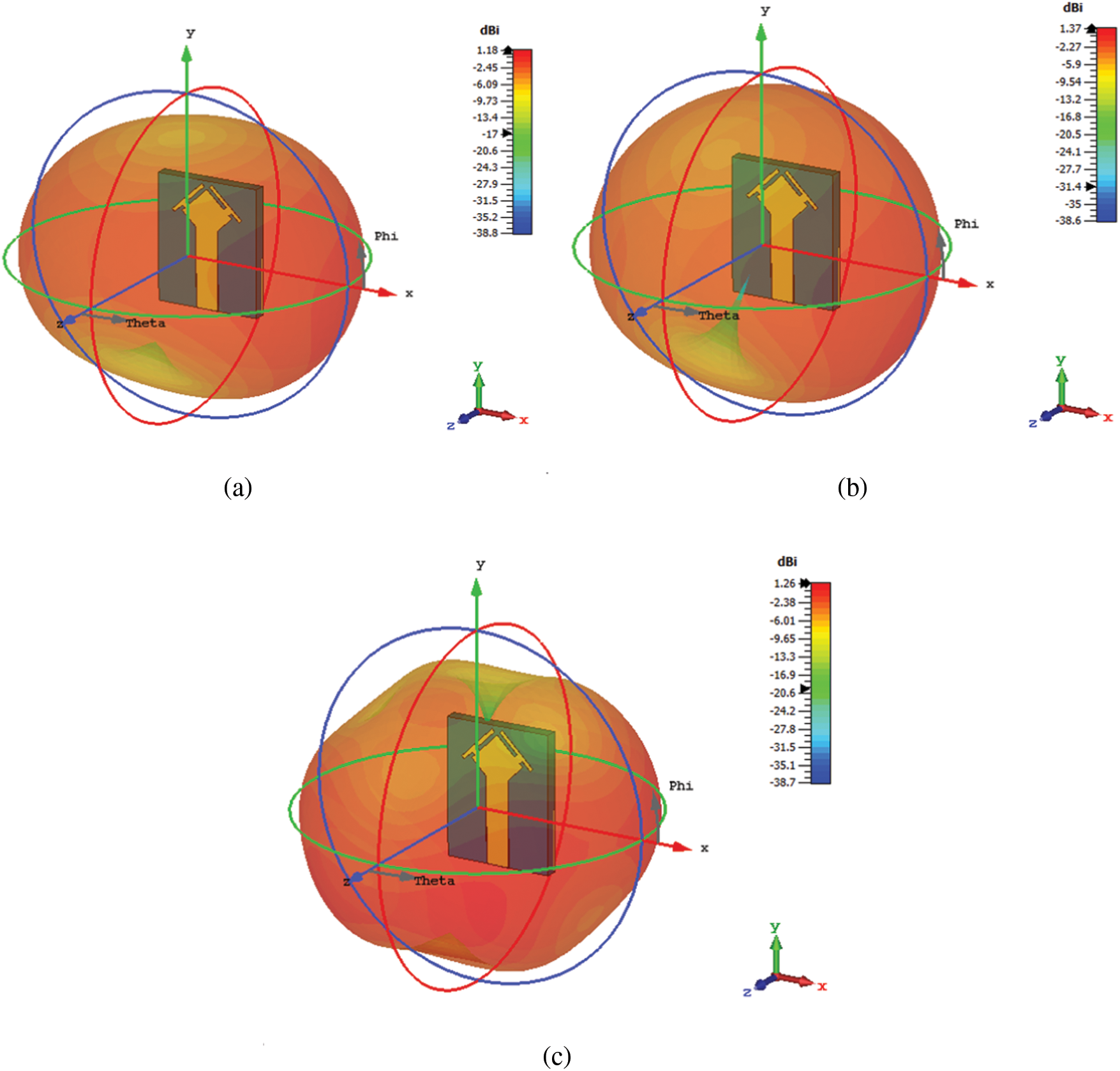
Figure 13: 3D Radiation pattern at (a) 4 GHz, (b) 5.5 GHz and (c) 10 GHz respectively
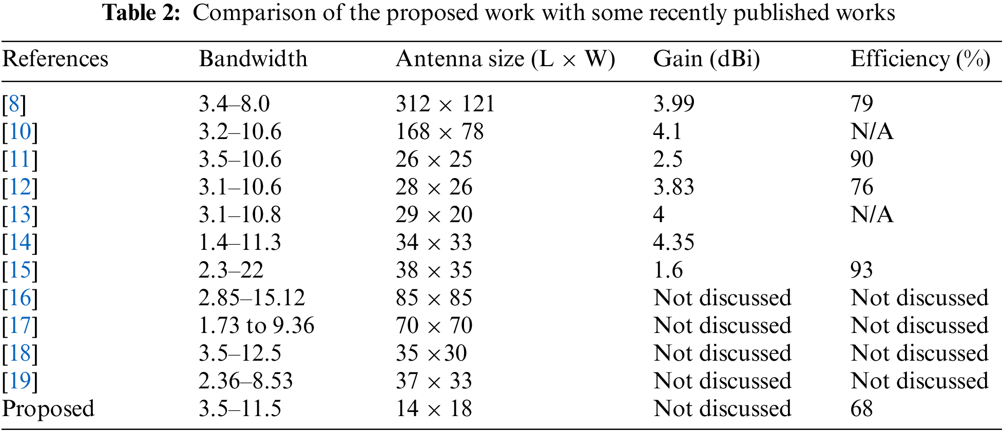
In Tab. 2, a comparison of the proposed antenna is made with some latest published works. Comparison is based on the achieved impedance bandwidth, antenna size gain and efficiencies. From the comparison table it is evident that the proposed design is very compact and has reasonable performance for UWB applications.
A compact rhombus shaped UWB antenna with truncated ground plane has been discussed in this work. For the wider impedance bandwidth, the proposed design has truncated ground plane with a rectangular notch in the ground plane. To enhance the impedance matching two stubs with two rectangular elements have been added to the tetrahedron shaped patch. The proposed design has an impedance band width of 8 GHz which start from 3.5 GHz till 11.5 GHz. The design has achieved a peak efficiency and gain of 68% and 1.5 dBi respectively. The design has a miniaturized size as compare to the published work. All these characteristics signify the proposed design suitability for the UWB applications.
Acknowledgement: We would like to give special thanks to Taif University Researchers supporting project number (TURSP-2020/216), Taif University, Taif, Saudi Arabia.
Funding Statement: Taif University Researchers are supporting project number (TURSP-2020/216), Taif University, Taif, Saudi Arabia.
Conflicts of Interest: The authors state that they have no conflicting interests to disclose in relation to this work.
1. S. R. Ahasan, K. Islam, M. M. Khan, M. Masud, G. S. Gaba et al., “Novel compact UWB band notch antenna design for body-centric communications,” Computer Systems Science and Engineering, vol. 40, no. 2, pp. 673–689, 2022. [Google Scholar]
2. J. Liang, C. C. Chiau, X. Chen and C. G. Parini, “Study of a printed circular disc monopole antenna for UWB systems,” IEEE Transactions on Antennas and Propagation, vol. 53, no. 11, pp. 3500–3504, 2005. [Google Scholar]
3. A. Haider, M. Rahman, H. Ahmad, M. N. Jahromi, M. T. Niaz et al., “Frequency-agile WLAN notch UWB antenna for URLLC applications,” Computers Materials & Continua, vol. 67, no. 2, pp. 2243–2254, 2021. [Google Scholar]
4. M. M. Khan, K. Islam, A. Shovon, M. Nakib, M. Baz et al., “Design of a novel 60 GHz millimeter wave Q-Slot antenna for body-centric communications,” International Journal of Antennas and Propagation, vol. 2021, no. 1, pp. 230–242, 2021. [Google Scholar]
5. V. N. K. R. Devana and A. M. Rao, “A compact flower slotted dual band notched ultra wideband antenna integrated with Ku band for ultra wideband, medical, direct broadcast service, and fixed satellite service applications,” Microwave and Optical Technology Letters, vol. 63, no. 2, pp. 556–563, 2021. [Google Scholar]
6. H. M. Rahman, M. M. Khan, M. Baz, M. Masud and M. A. AlZain, “Novel compact design and investigation of a super wideband millimeter wave antenna for body-centric communications,” International Journal of Antennas and Propagation, vol. 2021, no. 1, pp. 202–229, 2021. [Google Scholar]
7. K. Nakprasit, A. Sakonkanapong and C. Phongcharoenpanich, “Elliptical ring antenna excited by circular disc monopole for UWB communications,” International Journal of Antennas and Propagation, vol. 2020, no. 1, pp. 1–11, 2020. [Google Scholar]
8. J. N. Cruz, A. J. R. Serres, A. C. de Oliveira, G. V. R. Xavier, C. C. R. de Albuquerque et al., “Bio-inspired printed monopole antenna applied to partial discharge detection,” Sensors, vol. 19, no. 3, pp. 628–643, 2019. [Google Scholar]
9. S. A. Omar, A. Iqbal, O. Saraereh and A. Basir, “An array of M-shaped Vivaldi antennas for UWB applications,” Progress In Electromagnetics Research Letters, vol. 68, no. 1, pp. 67–72, 2017. [Google Scholar]
10. S. D. Ahirwar and C. Sairam, “Broadband corrugated square-shaped monopole antenna,” International Scholarly Research Notices, vol. 10, no. 1, pp. 9–19, 2011. [Google Scholar]
11. K. Islam, T. Hossain, M. M. Khan, M. Masud and R. Alroobaea, “Comparative design and study of A60 GHz antenna for body-centric wireless communications,” Computer Systems Science and Engineering, vol. 37, no. 1, pp. 19–32, 2019. [Google Scholar]
12. N. A. Jan, S. H. Kiani, F. Muhammad, D. A. Sehrai, A. Iqbal et al., “V-shaped monopole antenna with chichena itzia inspired defected ground structure for UWB applications,” Computers Materials & Continua, vol. 65, no. 1, pp. 19–32, 2020. [Google Scholar]
13. S. Zhang, Y. Zhong, Y. Zhou, Y. Guo and C. Ji, “Design of a symmetric open slot antenna for UWB applications,” IEICE Electronics Express, vol. 16, no. 20, pp. 1–13, 2019. [Google Scholar]
14. A. Iqbal, A. Smida, N. K. Mallat, M. T. Islam and S. Kim, “A compact UWB antenna with independently controllable notch bands,” Sensors, vol. 19, no. 6, pp. 1411–1424, 2019. [Google Scholar]
15. S. Ullah, C. Ruan, M. S. Sadiq, T. U. Haq and W. He, “High efficient and ultra wide band monopole antenna for microwave imaging and communication applications,” Sensors, vol. 20, no. 1, pp. 115–128, 2020. [Google Scholar]
16. A. K. Gautam, S. Yadav and B. K. Kanaujia, “A CPW-fed compact UWB microstrip antenna,” IEEE Antennas and Wireless Propagation Letters, vol. 12, pp. 1225–1536, 2013. [Google Scholar]
17. S. S. Bhatia and J. S. Sivia, “A novel design of circular monopole antenna for wireless applications,” Wireless Personal Communications, vol. 91, pp. 1153–1161, 2016. [Google Scholar]
18. M. Hayouni, F. Choubani, T. H. Vuong and J. David, “Main effects ensured by symmetric circular slots etched on the radiating patch of a compact monopole antenna on the impedance bandwidth and radiation patterns,” Wireless Personal Communications, vol. 95, no. 4, pp. 4243–4256, 2017. [Google Scholar]
19. L. C. Tsai and W. C. Lai, “Wideband CPW-Fed spiral shaped slot antenna for wireless applications,” Radio Electronics and Communications Systems, vol. 61, no. 4, pp. 180–183, 2018. [Google Scholar]
20. N. Sharma and S. S. Bhatia, “Ultra-wideband fractal antenna using rhombus shaped patch with stub loaded defected ground plane: Design and measuremet,” International Journal of Electronics and Communications, vol. 131, no. 4, pp. 58–65, 2021. [Google Scholar]
 | This work is licensed under a Creative Commons Attribution 4.0 International License, which permits unrestricted use, distribution, and reproduction in any medium, provided the original work is properly cited. |