DOI:10.32604/cmc.2022.029019
| Computers, Materials & Continua DOI:10.32604/cmc.2022.029019 | |
| Article |
Cache Memory Design for Single Bit Architecture with Different Sense Amplifiers
1VLSI Center of Excellence, GLA University, Mathura, 281406, India
2Computer Engineering Department, Research Chair of New Emerging Technologies and 5G Networks and Beyond, College of Computer and Information Sciences, King Saud University, Saudi Arabia
3Software Engineering Department, King Saud University, Riyadh, 11543, Saudi Arabia
4Al-Nahrain University, Al-Nahrain Nano-Renewable Energy Research Center, Baghdad, Iraq
5Applied College in Abqaiq, King Faisal University, Al-Ahsa, 31982, Saudi Arabia
*Corresponding Author: Reeya Agrawal. Email: agrawalreeya0304@gmail.com
Received: 22 February 2022; Accepted: 14 April 2022
Abstract: Most modern microprocessors have one or two levels of on-chip caches to make things run faster, but this is not always the case. Most of the time, these caches are made of static random access memory cells. They take up a lot of space on the chip and use a lot of electricity. A lot of the time, low power is more important than several aspects. This is true for phones and tablets. Cache memory design for single bit architecture consists of six transistors static random access memory cell, a circuit of write driver, and sense amplifiers (such as voltage differential sense amplifier, current differential sense amplifier, charge transfer differential sense amplifier, voltage latch sense amplifier, and current latch sense amplifier, all of which are compared on different resistance values in terms of a number of transistors, delay in sensing and consumption of power. The conclusion arises that single bit six transistor static random access memory cell voltage differential sense amplifier architecture consumes 11.34 μW of power which shows that power is reduced up to 83%, 77.75% reduction in the case of the current differential sense amplifier, 39.62% in case of charge transfer differential sense amplifier and 50% in case of voltage latch sense amplifier when compared to existing latch sense amplifier architecture. Furthermore, power reduction techniques are applied over different blocks of cache memory architecture to optimize energy. The single-bit six transistors static random access memory cell with forced tack technique and voltage differential sense amplifier with dual sleep technique consumes 8.078 μW of power, i.e., reduce 28% more power that makes single bit six transistor static random access memory cell with forced tack technique and voltage differential sense amplifier with dual sleep technique more energy efficient.
Keywords: Current differential sense amplifier (CDSA); voltage differential sense amplifier (VDSA); voltage latch sense amplifier (VLSA); current latch sense amplifier (CLSA); charge-transfer differential sense amplifier (CTDSA); new emerging technologies
Very-large-scale integrated circuit (VLSI) industries keep getting bigger, and the demand for mobile devices and battery-powered embedded systems is getting bigger and bigger all the time [1]. It takes up 60% to 70% of the chip area. As more chips are used, the speed of microprocessors slows down. Single-chip failure rates go up and down when a million transistors are on each chip. Cache memories now use more than half of a high-performance computer's transistors, which is expected to rise [2]. 6TSRAMC is the most common option for built-in stock because it is vital in chips like this that work well in noisy places. The design of low-power, high-performance processors, on the other hand, was given a lot of attention [3]. At some point, speed and power made things better. SA is an essential part of all 6TSRAMC memory blocks because it responds well to high frequency. It's the same for CMOS memories and other integrated circuits [4]. When there is more memory, the parasite space of the bit line tends to grow. In the last few years, the amount of memory that needs a lot of energy has kept going up. Cache memory is used to speed up synchronizing with a high-speed central processing unit (CPU). It is used as a CPU register because of its economic behaviour, even though it is costlier than the main memory. Cache memory is a buffer between the CPU and (random access memory) RAM, as the memory is high-speed [5]. It has data and instructions to easily and instantly accessible to the CPU. Cache memory is of two types, i.e., 6TSRAMC and dynamic random-access memory (DRAM). 6TSRAMC reduces the average time for data access and has a holding capacity of data than DRAM.
1.1 Low Power Reduction Techniques (LPRT)
This section discusses a small introduction of low power reduction techniques, including the working of techniques in the logic circuit and the working of transistors, as shown below [6].
1.1.1 Low Power Reduction Dual Sleep Technique
Space requirements for this technology are cut down because each transistor is replaced by three transistors, which takes up less space [7]. All logic circuits have a dual sleep component as standard. Schematic 1a illustrates that a specific logic circuit requires fewer transistors.
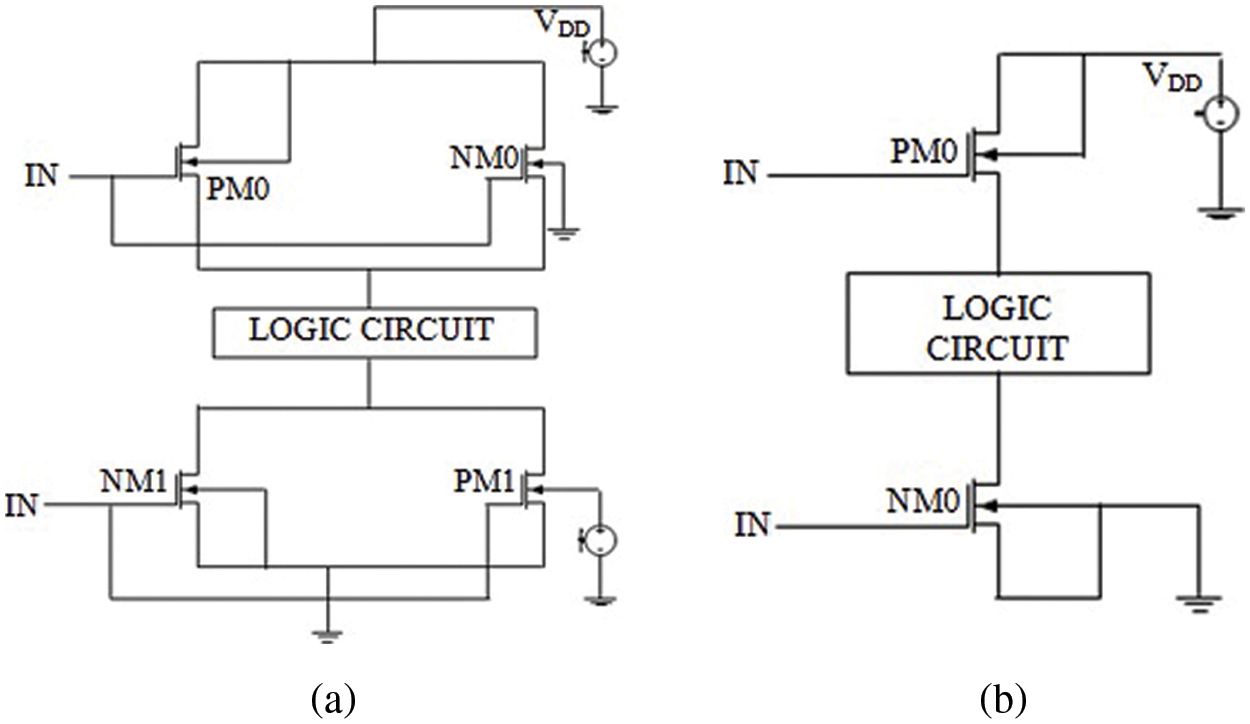
Schematic 1: (a) Low power reduction dual sleep technique circuit diagram, (b) Low power reduction sleep transistor technique circuit diagram
1.1.2 Low Power Reduction Sleep Transistor Technique
Low Power Reduction Sleep Transistor Technique is a well-known technique. It is also known as Power Reduction MTCMOS Technique. Schematic 1b [8] shows an extra sleep PMOS transistor between the VDD and the circuit pull-up network.
1.1.3 Low Power Reduction Forced Stack Technique
In the forced stack approach, instead of using a voltage supply, PM0 is utilized in the logic circuit, and instead of ground, NM0 is used, as illustrated in the Schematic 2a. Both MOS has the same input in this approach [9].
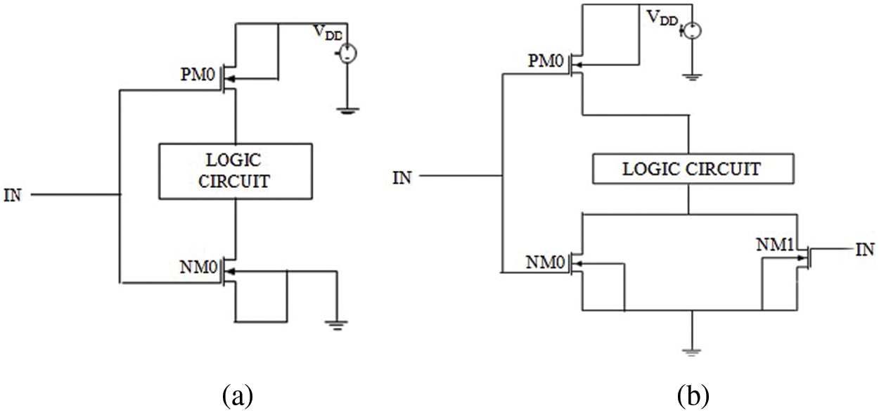
Schematic 2: (a) Low power reduction forced stack technique circuit diagram, (b) Low power reduction sleep stack technique circuit diagram
1.1.4 Low Power Reduction Sleep Stack Technique
Schematic 2b illustrates its structure. When both transistors are switched off simultaneously, the resulting reverse bias causes a sub-threshold reduction in leakage current. The sleepy stack approach was solved by integrating sleep and stacking methodologies [10].
Apart from the introduction, Section 2 covers related work in cache memory design for single-bit architecture. Section 3 describes a functional block diagram of cache memory design for single-bit architecture. Section 4 describes the proposed single bit 6TSRAMC SA architecture with its working and schematic. Section 5 describes simulated results with output waveforms and comparisons concerning the consumption of power, delay in sensing, and several transistors. Section 6 describes the summary of the paper in the form of a conclusion and future scope.
This section describes related work done in 6TSRAMC till 2022 by different authors’ papers. The conclusion arises from Tab. 1 that 6TSRAMC is the most popular in cache memory.
3 Cache Memory Design for Single Bit Architecture
They are creating a cache memory for single-bit architecture that allows for non-destructive reads and reliable writes. These two requirements collide when it comes to the size of 6TSRAMC transistors. 6TSRAMC transistor ratios must be followed for ad writing to be read successfully [31–33]. The main building blocks of the architectural blocks of ingle bit cache memory are described below. Schematic 3 shows the block diagram of cache memory design for single bit architecture.
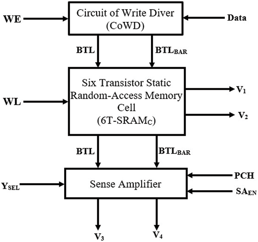
Schematic 3: Block diagram of cache memory design for single bit architecture
3.1 Circuit of Write Driver (CoWD) Working and Schematic
The CoWD function of the 6TSRAMC circuit is to rapidly discharge one of the bit-lines from pre-charge levels to below the 6TSRAMC write margin. Write Enable (WE) signal activates CoWD, which uses full-swing discharge to drive the bit line from the pre-charge stage to the ground [34]. As illustrated in Schematic 4, the order in which word line (WL) is authorized and CoWD is triggered is unimportant for the proper writing process.
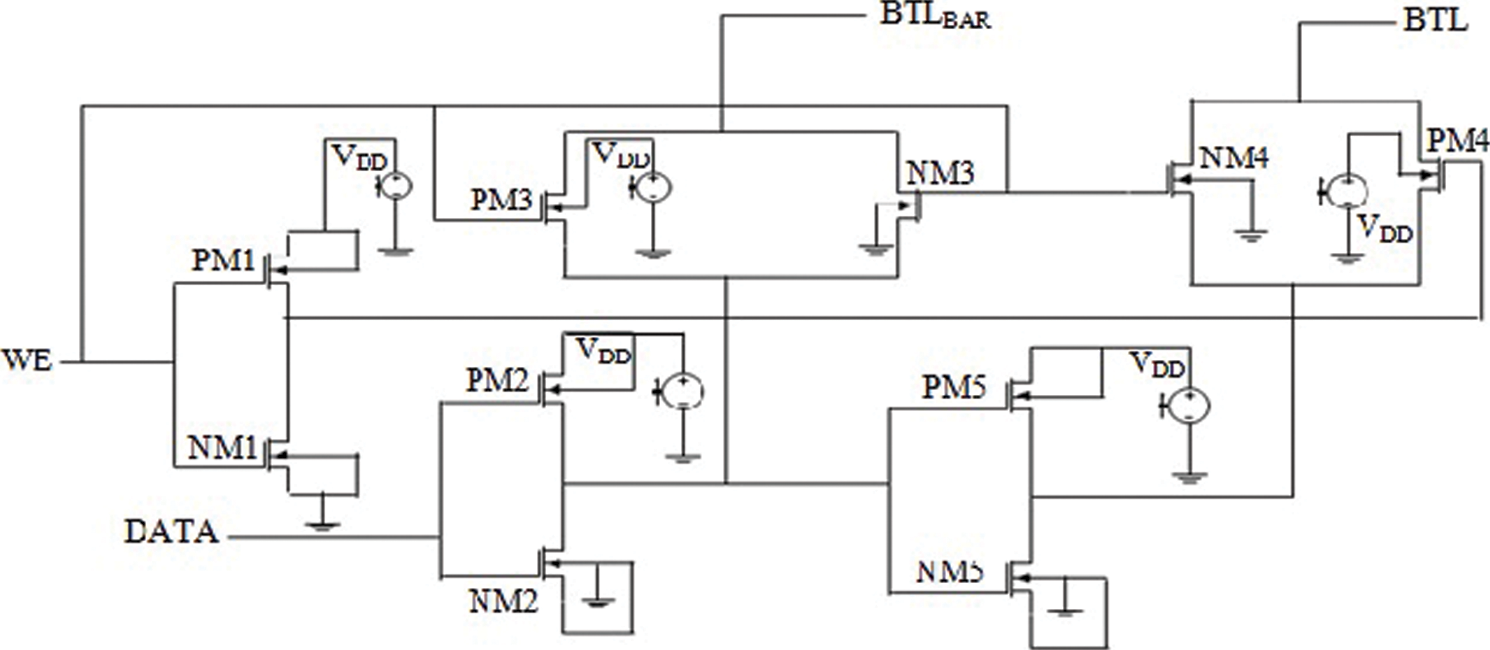
Schematic 4: CoWD circuit diagram
3.2 Six-Transistor Static Random Access Memory (6TSRAMC) Working and Schematic
The design of 6TSRAMC is essential for the safe and robust functioning of the architecture. The 6TSRAMC must be small, stable, robust, and yield constraints—binary data storage by a 6TSRAMC portion [35]. The word line defines modes of operation. When all transistors are removed, and cells are separated. The word line pulls high for reading and writing functions that enable access transistors (NM8 and NM9).
A typical 6TSRAMC uses two cross-connected inverters, which create a transistor lock and access [36]. Access transistors (NM8 and NM9) allow reading and writing to the cell and provide cell isolation when the cell is not accessible, as shown in the Schematic 5.
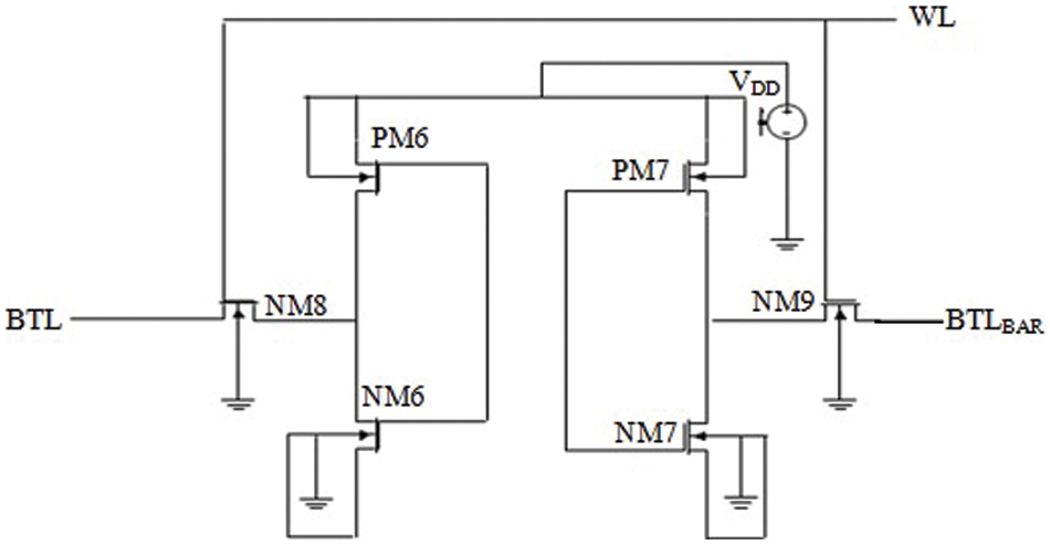
Schematic 5: 6TSRAMC circuit diagram
SA is a vital memory design aspect. SA's preference and configuration determine the robustness of bit-line detection, which impacts readability and power [37–39]. Sensing operation must be non-destructive, provided that 6TSRAMCs need no data to refresh circuits after sensing.
4 Proposed Single Bit 6TSRAMC SA Architecture
In this section, all the proposed architecture schematic has been shown as well as the working of all the architecture has been defined below [40].
4.1 Single Bit 6TSRAMC VDSA Architecture Working and Schematic
Voltage Differential Sense Amplifier (VDSA) detects the bit-line differential voltage and generates a total rail output. The circuit is depicted in Schematic 6. The BTL and BTLBAR pair create a voltage difference when WL = high. When SAEN = high, when the required differential is reached, the cross-coupled inverter enters a positive feedback loop [41].
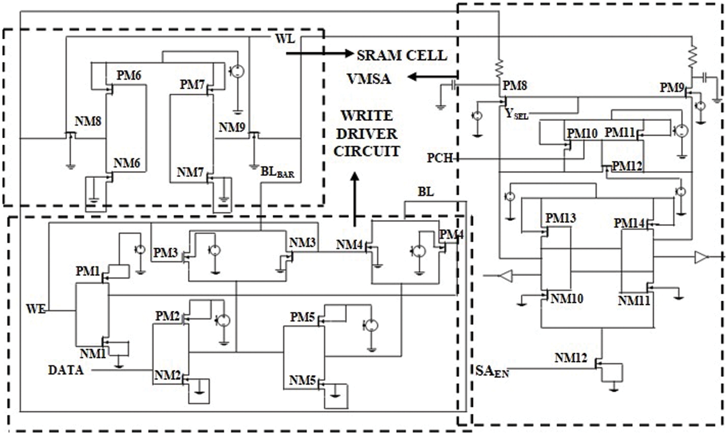
Schematic 6: Single bit 6TSRAMC VDSA architecture circuit diagram
The bit-line connected SA output node is set to zero, while the other output SA1 is kept raised with a lower voltage, e.g., SA2. When the sensing amplifier is turned on, NM10 and NM11 become saturated. The NM11 device has a greater VDD input voltage than the NM10, with a lower Vgs voltage. The more significant current (NM11) results in a lower output voltage on the other NM10 device, lowering Vgs and resulting in a lower current [42].
4.2 Single Bit 6TSRAMC CDSA Architecture Working and Schematic
The circuit architecture for a current detecting amplifier is shown in the Schematic 7. CDSA operates by directly measuring bit-cell current. It does not rely on developing a different voltage across the bit-line [43,44]. The lower bit-line can be clamped at a greater voltage in an amplifier voltage sense. As a consequence, bit-line power pre-charge can be minimized. CDSA has two components: a transmitting circuit with unit transmission characteristics and a sensing circuit that monitors the differential current. Pre-charge and assessment are two tasks of the current mode sensing amplifier [45,46].
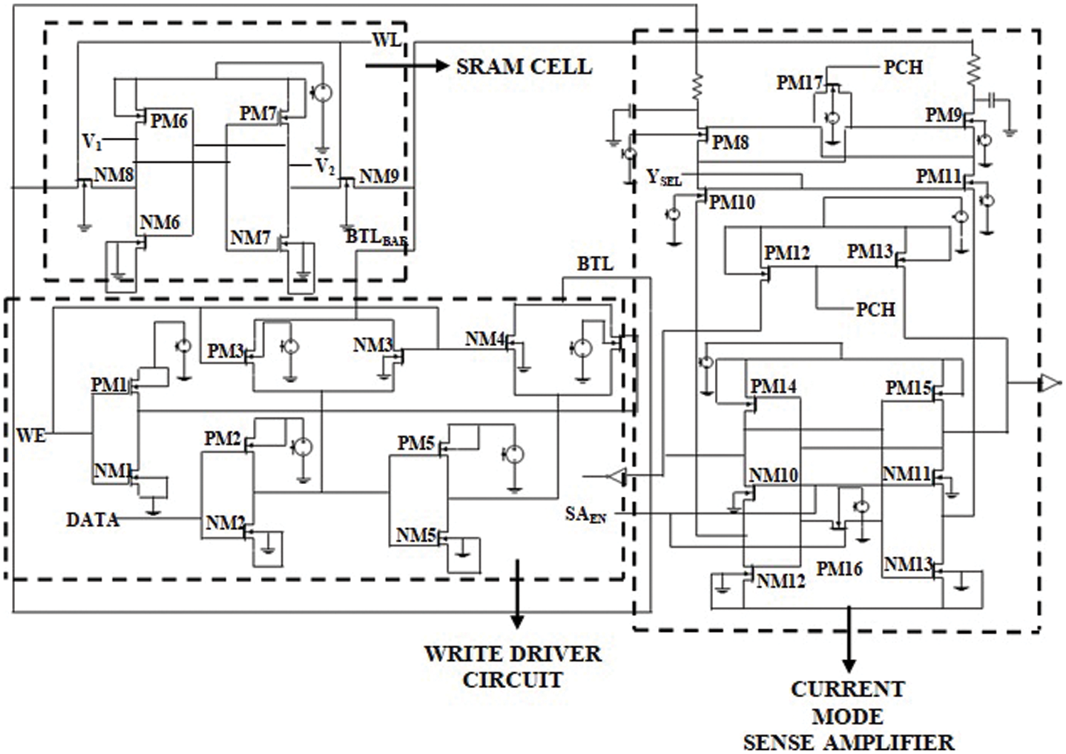
Schematic 7: Single bit 6TSRAMC CDSA architecture circuit diagram
4.3 Single Bit 6TSRAMC CTDSA Architecture Working and Schematic
The circuit diagram of a CTDSA is shown in Schematic 8. Load transfer amplification aims to increase voltage gain by utilizing load conservation across capacitive systems [47]. A charge is transferred from high-capacity bit lines to low-capacity amplifier output nodes in the CTDSA. The minimal voltage swing of the bit-lines results in faster speeds and reduced energy usage.
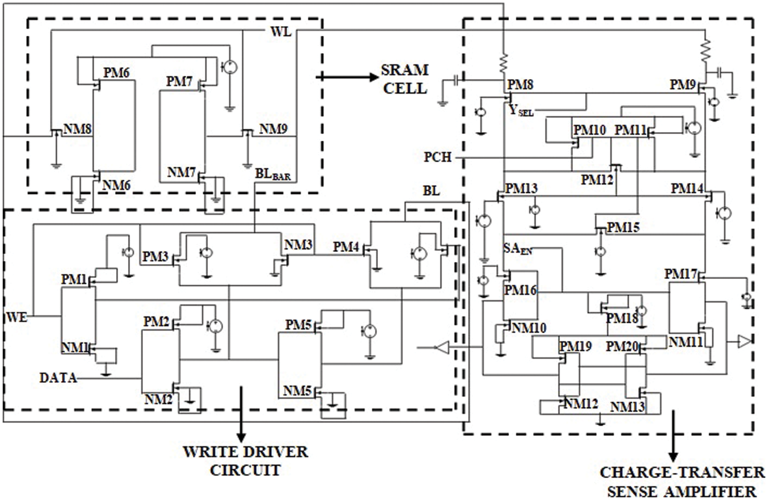
Schematic 8: Single bit 6TSRAMC CTDSA architecture circuit diagram
4.4 Single Bit 6TSRAMC VLSA Architecture Working and Schematic
This study created the voltage latch sense amplifier (VLSA) schematics in this study in Schematic 9. The bit-lines are used to pre-charge the internal nodes of this architecture. The circuit design employs the input bit-lines based on internal nodes [48,49].
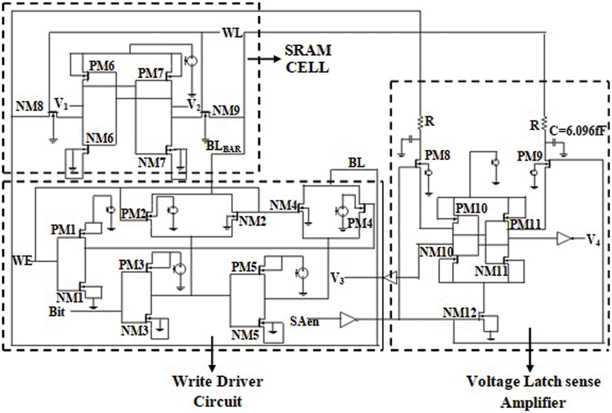
Schematic 9: Single bit 6TSRAMC VLSA architecture circuit diagram
When the word line is pushed high and before the sense amplifier signal, NM12 is turned off, and PM8 and PM9 pass transistors are turned on. The random bit on the internal nodes of the sense amplifier has an appropriate voltage difference as the differential on the bit lines grows. A differential voltage is amplified to its maximum swing output when the SAEN sensing amplifier signal is asserted [50,51].
4.5 Single Bit 6TSRAMC CLSA Architecture Working and Schematic
One of the bit lines releases throughout the reading operation, while the other remains at supply voltage. Due to the capabilities of a big bit-line, the slow discharge is moderate, and the bit cells have access to the transistor [52–54].
SA does this by amplifying a slight change in the bit line voltages at digital levels. CLSA schematic is shown in Schematic 10. The differential voltage is carried via bit-lines to the CLSA inputs SA3 and SA4. If SA1 and SA2 begin to discharge at high levels, SAEN is pulled high [55–58].
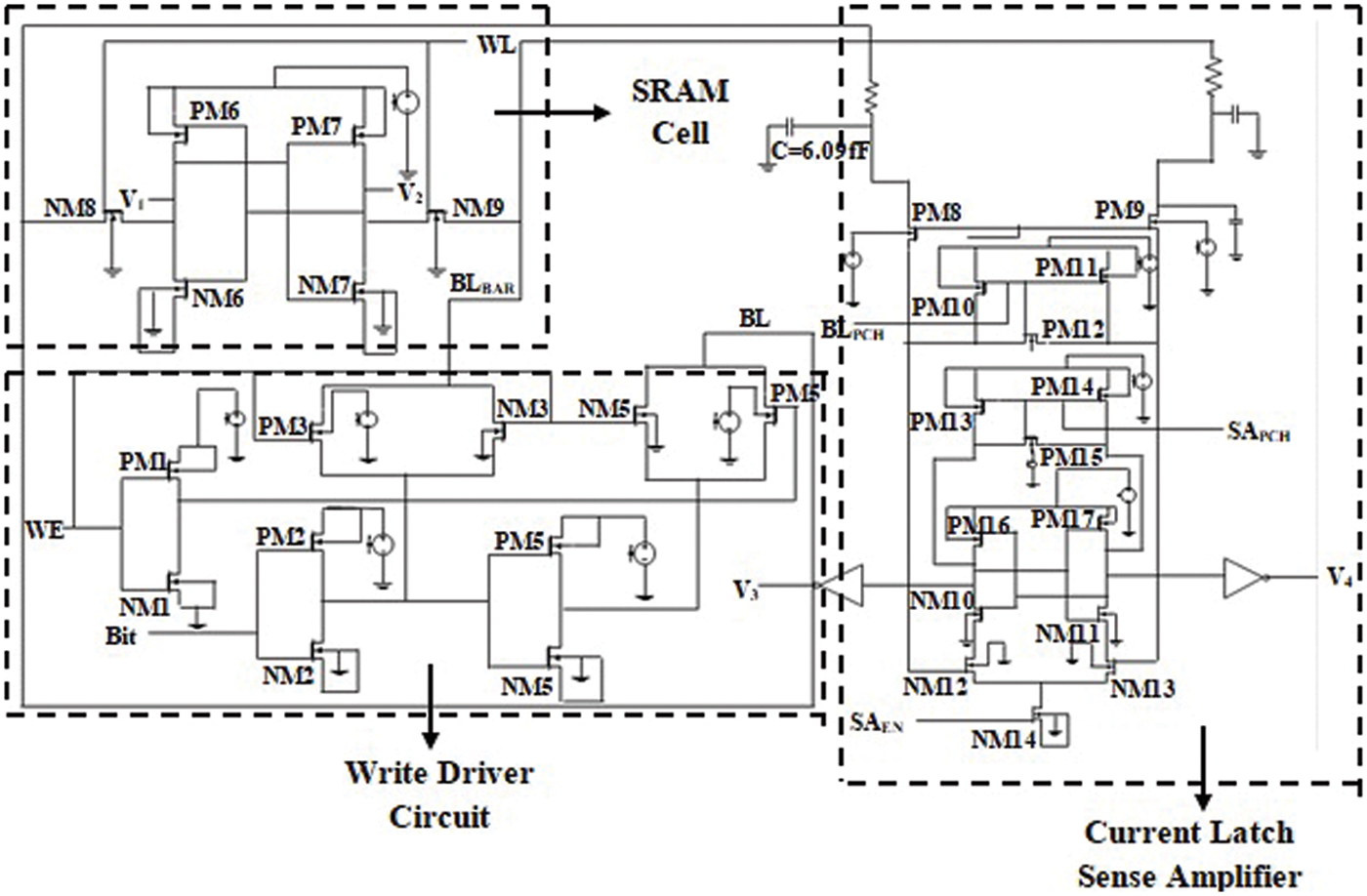
Schematic 10: Single bit 6TSRAMC CLSA architecture circuit diagram
The power consumption of all the circuits has been analyzed in this section. Tabs. 2 and 3 describe a single bit 6TSRAMC SA architecture with different parameters using different types of SA's such as (VDSA, CDSA, CTDSA, VLSA, and CLSA) at additional values of resistance (such as 42.3 Ω and 42.3 kΩ) with other parameters such as delay in sensing, several transistors and consumption of power.

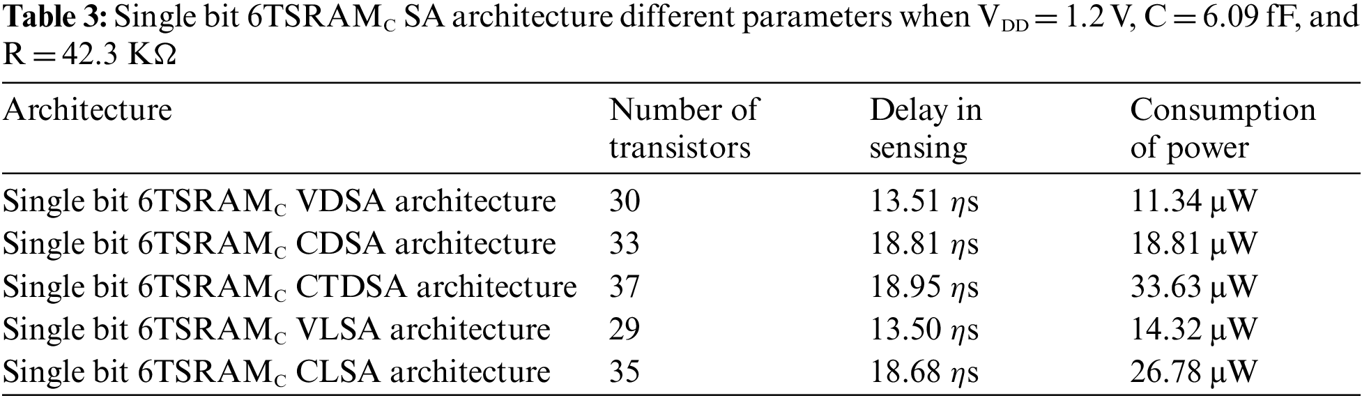
From Tabs. 2 and 3, conclusions arise that singe bit 6TSRAMC VDSA architecture consumes 11.34 μW of power, the lowest among all the architectures. Due to this reason, LPRT has been applied over a single bit 6TSRAMC VDSA architecture, but there is an increment in the number of the transistor.
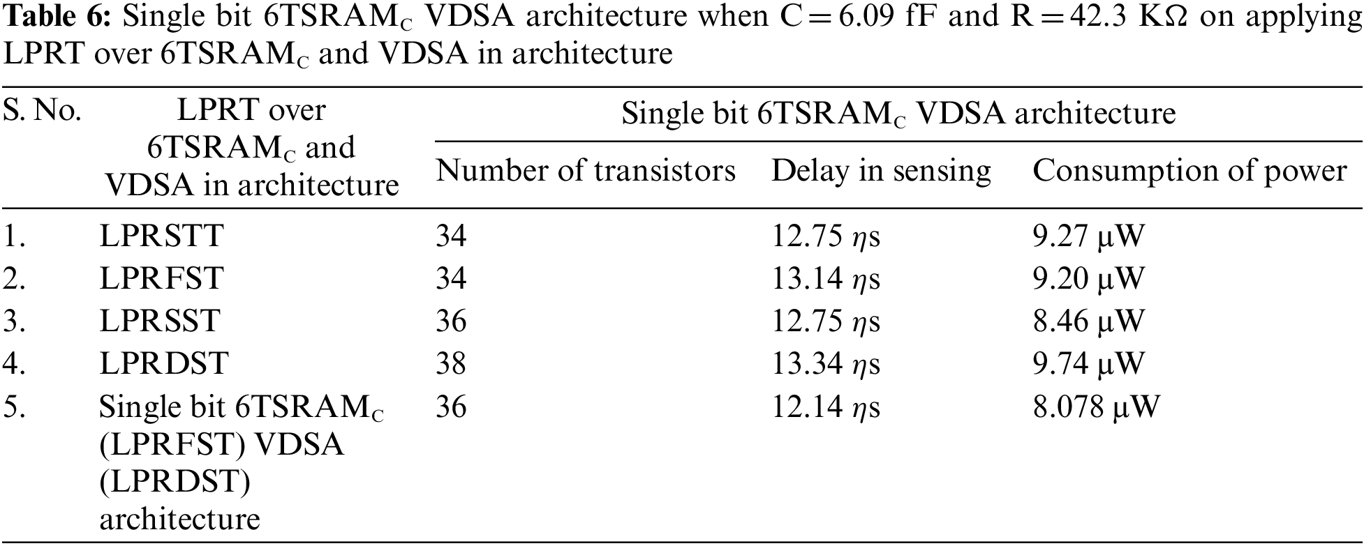
Tab. 4 describes different parameters of single bit 6TSRAMC VDSA architecture, and to optimize the consumption of power, techniques of power reduction are applied over VDSA. Tab. 5 describes that using LPRT over 6TSRAMC in single bit 6TSRAMC VDSA architecture also reduces the consumption of power. Due to this, there is an increment in the number of transistors in the design.
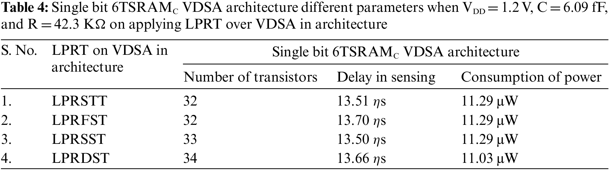
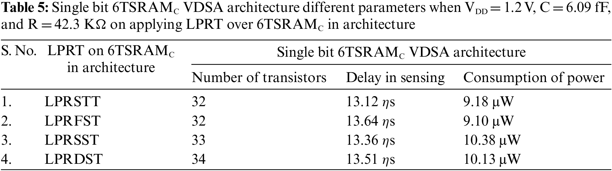
From Tabs. 4 and 5, conclusions arise that Singe Bit 6TSRAMC with LPRFST VDSA with LPRDST consumes 8.078 μW of power, which is the lowest compared to others. Schematic 11 shows the proposed schematic of single bit 6TSRAMC with LPRFST VDSA with LPRDST architecture schematic.
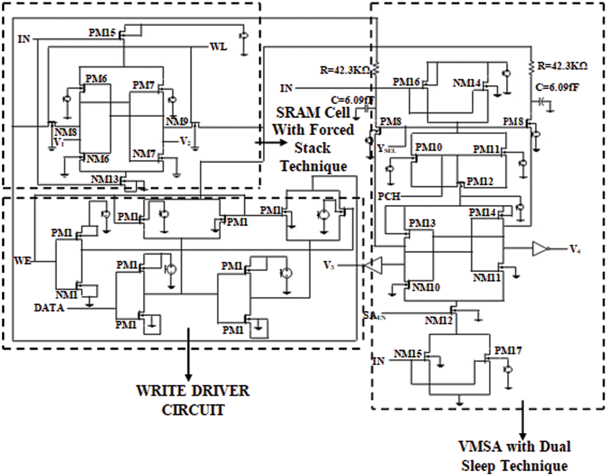
Schematic 11: Single bit 6TSRAMC with LPRFST VDSA with LPRDST architecture circuit diagram
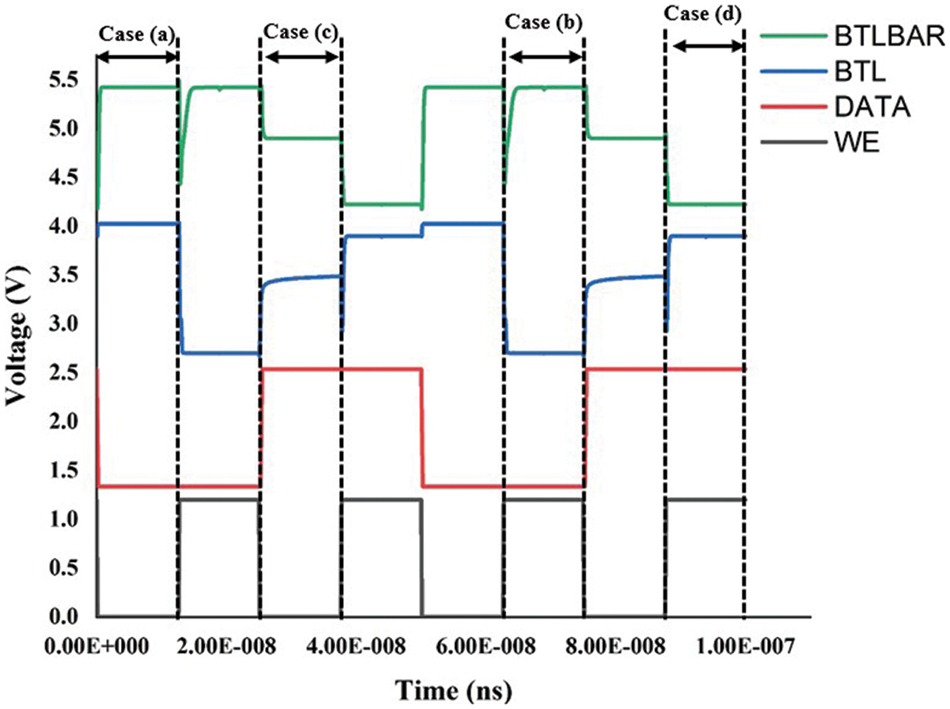
Schematic 12 shows the output waveform of CoWD, where WE and Data are inputs, and BTL and BTLBAR are output are described in four cases.
Schematic 12: CoWD output waveform
Case (a): WE and Data both are low, BTL and BTLBAR both are high, while,
Case (b): WE are high, Data is low, BTL is low, and BTLBAR is high,
Case (c): Data is high, and WE are low, BTL and BTLBAR are high/2,
Case (d): Data is high, WE are high, BTL is high, and BTLBAR is low.
Schematic 13 shows the output waveform of 6TSRAMC, which shows the write operation and hold operation held in the 6TSRAMC. Schematic 14 shows the output waveform of single bit 6TSRAMC VDSA architecture, i.e., reading operation done by a SA that reads the store data in 6TSRAMC. Tab. 6 describes applying LPRT over different blocks of cache memory design for single bit architecture (such as 6TSRAMC and VDSA) to optimize power consumption. Results depicted that single bit 6TSRAMC with LPRFST VDSA with LPRDST architecture consumes 8.078 μW of power which is the lowest as compared to architecture. But due to this, there is an increment in the number of transistors.
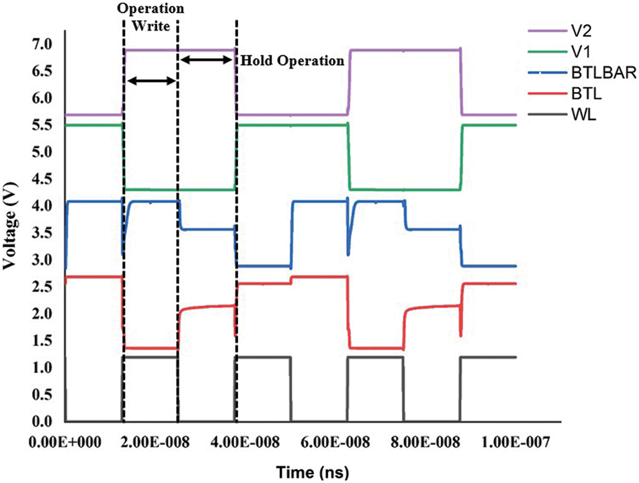
Schematic 13: 6TSRAMC output waveform
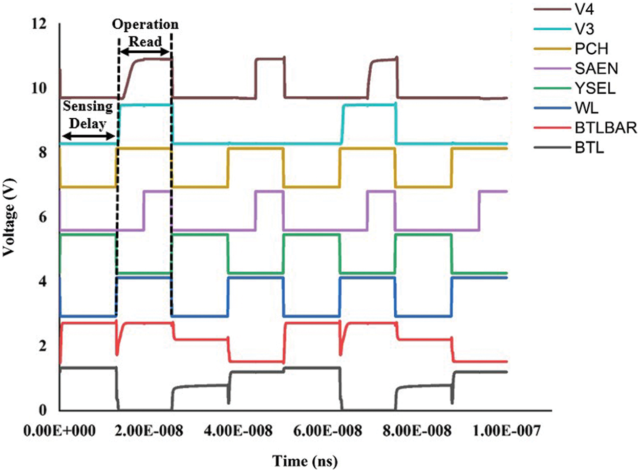
Schematic 14: Single bit 6TSRAMC VDSA architecture
In this paper, cache memory design for single-bit architecture with different sense amplifiers has been implemented and analyzed. Single Bit 6TSRAMC SA Architecture comprises CoWD, 6TSRAMC, and SA (VDSA, CDSA, CTDSA, VLSA, and CLSA). All architectures are compared on different values of resistance (R) with other parameters such as consumption of power, delay in sensing and number of transistors. Results showed that single bit six transistor static random access memory cell voltage differential sense amplifier architecture consumes 11.34 μW of power. Furthermore, LPRT is applied over different cache memory architecture blocks to optimize power. The single-bit 6TSRAMC with LPRFST and VDSA with LPRDST consume 8.078 μW of power, i.e., reduce 28% more ability and make it more efficient.
Future Scope–This work can be done in the form of the array, and LPRT can be applied to other architectures. Moreover, other sense amplifiers can be used in architecture to reduce the drawbacks of the proposed architecture; Apart from it, these architectures can be compared over different parameters such as read delay, write delay, signal to noise margin etc.
Author Contributions: A short paragraph specifying their contributions must be provided for research articles with several authors. The following statements should be used “Conceptualization, Reeya Agrawal; methodology, Reeya Agrawal; software, cadence tool; validation, Reeya Agrawal, Anjan Kumar Salman; formal analysis, Reeya Agrawal; investigation, Reeya Agrawal; resources, Reeya Agrawal; data curation, Reeya Agrawal; writing—original draft preparation, Reeya Agrawal; writing—review and editing, Anjan Kumar; visualization, Osamah Ibrahim Khalif; supervision, Salman; project administration. All authors have read and agreed to the published version of the manuscript.
Acknowledgement: Authors are grateful to the Deanship of Scientific Research at King Saud University for funding this work through the Vice Deanship of Scientific Research Chairs: Research Chair of New Emerging Technologies 5G Networks and Beyond.
Funding Statement: Research General Direction funded this research at Universidad Santiago de Cali, Grant Number 01-2021 and APC was funded by 01-2021.
Conflicts of Interest: The authors declare that they have no conflicts of interest to report regarding the present study.
1. P. Görgel, “Greedy segmentation based diabetic retinopathy identification using curvelet transform and scale invariant features,” Journal of Engineering Research, vol. 9, no. 1, pp. 134–150, 2021. [Google Scholar]
2. H. Bazzi, A. Harb, H. Aziza, M. Moreau and A. Kassem, “RRAM-based non-volatile SRAM cell architectures for ultra-low-power applications,” Analog Integrated Circuits and Signal Processing, vol. 106, no. 2, pp. 351–361, 2021. [Google Scholar]
3. X. Zhang, W. Zhang, W. Sun, X. Sun and S. K. Jha, “A robust 3-D medical watermarking based on wavelet transform for data protection,” Computer Systems Science and Engineering, vol. 41, no. 3, pp. 1043–1056, 2022. [Google Scholar]
4. Q. Zhang, J. Gao, J. T. Wu, Z. Cao and D. Dajun Zeng, “Data science approaches to confronting the COVID-19 pandemic: A narrative review,” Philosophical Transactions of the Royal Society A, vol. 380, no. 2214, pp. 20210127, 2022. [Google Scholar]
5. X. Wang, J. Liu, X. Liu, Z. Liu and O. I. Khalaf et al., “Ship feature recognition methods for deep learning in complex marine environments,” Complex & Intelligent Systems, pp. 1–17, 2022. https://doi.org/10.1007/s40747-022-00683-z. [Google Scholar]
6. W. Wang, U. Guin and A. Singh, “Aging-resilient SRAM-based true random number generator for lightweight devices,” Journal of Electronic Testing, vol. 36, no. 3, pp. 301–311, 2020. [Google Scholar]
7. Y. He, J. Zhang, X. Wu, X. Si and S. Zhen et al., “A half-select disturb-free 11 T SRAM cell with built-in write/read-assist scheme for ultralow-voltage operations,” IEEE Transactions on Very Large Scale Integration (VLSI) Systems, vol. 27, no. 10, pp. 2344–2353, 2019. [Google Scholar]
8. R. Fragasse, R. Tantawy, B. Dupaix, T. Dean and D. DiSabato et al., “Analysis of SRAM enhancements through sense amplifier capacitive offset correction and replica self-timing,” IEEE Transactions on Circuits and Systems I: Regular Papers, vol. 66, no. 6, pp. 2037–2050, 2019. [Google Scholar]
9. S. Gupta, K. Gupta, B. H. Calhoun and N. Pandey, “Low-power near-threshold 10 T SRAM bit cells with enhanced data-independent read port leakage for array augmentation in 32-nm CMOS,” IEEE Transactions on Circuits and Systems I: Regular Papers, vol. 66, no. 3, pp. 978–988, 2018. [Google Scholar]
10. K. Oladosu, A. Mustapha, M. Durowoju and O. Ogunsanya, “Performance evaluation of combustion of palm kernel shell and coconut husk blend in a pilot scale grate furnace,” Journal of Engineering Research, vol. 9, no. 1, pp. 1–12, 2021. [Google Scholar]
11. R. Zhang, K. Yang, Z. Liu, T. Liu, W. Cai and L. Milor, “A comprehensive framework for analysis of time-dependent performance-reliability degradation of SRAM cache memory,” IEEE Transactions on Very Large Scale Integration (VLSI) Systems, vol. 29, no. 5, pp. 857–870, 2021. [Google Scholar]
12. C. Roy, and A. Islam, “Design of low power, variation tolerant single bitline 9 T SRAM cell in 16-nm technology in subthreshold region,” Microelectronics Reliability, vol. 120, pp. 114126, 2021. [Google Scholar]
13. S. Mittal, G. Verma, B. Kaushik and F. A. Khanday, “A survey of SRAM-based in-memory computing techniques and applications,” Journal of Systems Architecture, vol. 119, pp. 102276, 2021. [Google Scholar]
14. K. Gavaskar, M. S. Narayanan, M. S. Nachammal and K. Vignesh, “Design and comparative analysis of SRAM array using low leakage controlled transistor technique with improved delay,” Journal of Ambient Intelligence and Humanized Computing, pp. 1–10, 2021. https://doi.org/10.1007/s12652-021-03353-z. [Google Scholar]
15. R. C. Aparna, “A study of different SRAM cell designs,” International Journal, vol. 9, no. 3, pp. 303–309, 2021. [Google Scholar]
16. R. Agrawal, “Cache memory design for single bit architecture for IoT applications,” in 5th Int. Conf. on Information Systems and Computer Networks (ISCON), pp. 1–4, 2021. https://doi.org.10.1109/ISCON52037.2021.9702515. [Google Scholar]
17. J. Dinesh Kumar, C. Ganesh Babu, V. Balaji, K. Priyadharsini and S. Karthi, “Performance investigation of various SRAM cells for IoT based wearable biomedical devices,” in Inventive Communication and Computational Technologies, Singapore, Springer, pp. 573–588, 2021. [Google Scholar]
18. K. Neeraj, M. M. Basha and S. Gundala, “Design of low power SRAM-based ubiquitous sensor for wireless body area networks,” International Journal of Pervasive Computing and Communications, vol. 17, no. 5, pp. 611–621, 2021. [Google Scholar]
19. T. V. Lakshmi, and M. Kamaraju, “Implementation of high performance 6 T-SRAM cell,” Journal of Physics: Conference Series, vol. 1804, no. 1, pp. 012185, 2021. [Google Scholar]
20. O. Mohana Chandrika and M. Siva Kumar, “Design and analysis of SRAM cell using reversible logic gates towards smart computing,” the Journal of Supercomputing, vol. 78, pp. 2287–2306, 2021. [Google Scholar]
21. T. Sargunam, C. Prabhu and L. W. Soong, “Design of novel low power (NLP) SRAM cell for wireless sensor network applications,” ARPN Journal of Engineering and Applied Sciences, vol. 16, no. 7, pp. 762–770, 2021. [Google Scholar]
22. Y. Kim, S. Patel, H. Kim, N. Yadav and K. K. Choi, “Ultra-low power and high-throughput SRAM design to enhance AI computing ability in autonomous vehicles,” Electronics, vol. 10, no. 3, pp. 256, 2021. [Google Scholar]
23. G. Munirathnam and Y. M. M. Babu, “Analysis of static power reduction strategies in deep submicron CMOS device technology for digital circuits,” in 2021 6th International Conference on Signal Processing, Computing and Control (ISPCC), pp. 278–282, 2021. https://doi.org.10.1109/ISPCC53510.2021.9609444. [Google Scholar]
24. C. J. Liu, Y. Wan, L. J. Li, C. P. Lin and T. H. Hou et al., “Two-dimensional materials-based static random-access memory,” in Advanced Materials, pp. 2107894, 2021. https://doi.org/10.1002/adma.202107894. [Google Scholar]
25. Y. Wang, Z. Wang and L. Zhang, “A new 6-transistor SRAM cell for low power cache design,” in 11th Int. Conf. on Solid-State and Integrated Circuit Technology, pp. 1–3, 2012. https://doi.org/10.1109/ICSICT.2012.6467902. [Google Scholar]
26. M. Gupta, K. Gupta and N. Pandey, “Comparative analysis of the design techniques for low leakage SRAMs at 32 nm,” Microprocessors and Microsystems, vol. 85, pp. 104281, 2021. [Google Scholar]
27. K. R, S. T, V. N, S. B and S. A, “Design of a sleep transistor and read, write separation based 6 T SRAM memory array for low power IOT applications,” Smart Technologies, Communication and Robotics (STCR), pp. 1–5, 2021. https://doi.org.10.1109/STCR51658.2021.9588951. [Google Scholar]
28. P. Huang, K. C. Chang, J. Ge, C. Peng and X. Wu et al., “Offset-compensation high-performance sense amplifier for low-voltage DRAM based on current mirror and switching point,” IEEE Transactions on Circuits and Systems II: Express Briefs, vol. 69, no. 4, pp. 2011–2015, 2022. [Google Scholar]
29. C. A. Kumar, B. K. Madhavi and K. Lalkishore, “Performance analysis of low power 6 T SRAM cell in 180 nm and 90 nm,” in 2nd Int. Conf. on Advances in Electrical, Electronics, Information, Communication and Bio-Informatics (AEEICB), pp. 351–357, 2016. https://doi.org.10.1109/AEEICB.2016.7538307. [Google Scholar]
30. M. Nouripayam, A. Prieto, V. K. Kishorelal and J. Rodrigues, “An energy-efficient near-memory computing architecture for CNN inference at cache level,” in 28th IEEE Int. Conf. on Electronics, Circuits, and Systems (ICECS), pp. 1–4, 2021. https://doi.org.10.1109/ICECS53924.2021.9665530. [Google Scholar]
31. R. Agrawal and V. K. Tomar, “Implementation and analysis of Low power reduction techniques in sense amplifier,” in Second Int. Conf. on Electronics, Communication and Aerospace Technology (ICECA), pp. 439–444, 2018. https://doi.org.10.1109/ICECA.2018.8474703. [Google Scholar]
32. Y. Tao and W. Hu, “Design of sense amplifier in the high speed SRAM,” in Int. Conf. on Cyber-Enabled Distributed Computing and Knowledge Discovery, pp. 384–387, 2015. https://doi.org.10.1109/CyberC.2015.32. [Google Scholar]
33. O. I. Khalaf and G. M. Abdulsahib, “Design and performance analysis of wireless IPv6 for data exchange,” Journal of Information Science & Engineering, vol. 37, no. 6, pp. 1335–1340, 2021. [Google Scholar]
34. M. Jefremow, T. Kern, W. Allers, C. Peters and J. Otterstedt et al., “Time-differential sense amplifier for sub-80 mV bitline voltage embedded STT-MRAM in 40 nm CMOS,” IEEE International Solid-State Circuits Conference Digest of Technical Papers, pp. 216–217, 2013. https://doi.org.10.1109/ISSCC.2013.6487706. [Google Scholar]
35. R. Agrawal and V. K. Tomar, “Analysis of Low power reduction techniques on cache (SRAM) memory,” in 9th Int. Conf. on Computing, Communication and Networking Technologies (ICCCNT), pp. 1–7, 2018. https://doi.org.10.1109/ICCCNT.2018.8494021. [Google Scholar]
36. N. A. Khan, O. Ibrahim Khalaf, C. Andrés Tavera Romero, M. Sulaiman and M. A. Bakar, “Application of intelligent paradigm through neural networks for numerical solution of multiorder fractional differential equations,” Computational Intelligence and Neuroscience, vol. 2022, pp. 2710576, 2022. [Google Scholar]
37. R. Dutt and M. Abhijeet, “High speed current mode sense amplifier for sram applications,” IOSR Journal of Engineering, vol. 2, no. 5, pp. 1124–1127, 2012. [Google Scholar]
38. U. Srilakshmi, N. Veeraiah, Y. Alotaibi, S. A. Alghamdi and O. I. Khalaf et al., “An improved hybrid secure multipath routing protocol for MANET,” IEEE Access, vol. 9, pp. 163043–163053, 2021. [Google Scholar]
39. S. Rajendran, O. I. Khalaf, Y. Alotaibi and S. Alghamdi, “MapReduce-based big data classification model using feature subset selection and hyperparameter tuned deep belief network,” Scientific Reports, vol. 11, no. 1, pp. 1–10, 2021. [Google Scholar]
40. A. R. Khaparde, F. Alassery, A. Kumar, Y. Alotaibi, O. I. Khalaf et al., “Differential evolution algorithm with hierarchical fair competition model,” Intelligent Automation & Soft Computing (Tech Science Press), vol. 33, no. 2, pp. 1045–1062, 2022. [Google Scholar]
41. R. Agrawal, “Low-power SRAM memory architecture for IoT Systems,” in Recent Advances in Manufacturing, Automation, Design and Energy Technologies, Singapore, Springer, pp. 505–512, 2022. [Google Scholar]
42. H. Rödjegård and A. Lööf, “A differential charge-transfer readout circuit for multiple output capacitive sensors,” Sensors and Actuators A: Physical, vol. 119, no. 2, pp. 309–315, 2005. [Google Scholar]
43. T. Na, S. H. Woo, J. Kim, H. Jeong and S. O. Jung, “Comparative study of various latch-type sense amplifiers,” IEEE Transactions on Very Large Scale Integration (VLSI) Systems, vol. 22, no. 2, pp. 425–429, 2013. [Google Scholar]
44. O. I. Khalaf and G. M. Abdulsahib, “Optimized dynamic storage of data (ODSD) in IoT based on blockchain for wireless sensor networks,” Peer-to-Peer Networking and Applications, vol. 14, no. 5, pp. 2858–2873, 2021. [Google Scholar]
45. S. S. Rawat, S. Alghamdi, G. Kumar, Y. Alotaibi and O. I. Khalaf et al., “Infrared small target detection based on partial sum minimization and total variation,” Mathematics, vol. 10, no. 4, pp. 671, 2022. [Google Scholar]
46. P. Mohan, N. Subramani, Y. Alotaibi, S. Alghamdi and O. I. Khalaf et al., “Improved metaheuristics-based clustering with multihop routing protocol for underwater wireless sensor networks,” Sensors, vol. 22, no. 4, pp. 1618, 2022. [Google Scholar]
47. D. Arora, A. K. Gundu and M. S. Hashmi, “A high speed low voltage latch type sense amplifier for non-volatile memory,” in 20th Int. Symp. on VLSI Design and Test (VDAT), Guwahati, India, pp. 1–5, 2016. [Google Scholar]
48. T. Puri, M. Soni, G. Dhiman, O. Ibrahim Khalaf and I. Raza Khan, “Detection of emotion of speech for RAVDESS audio using hybrid convolution neural network,” Journal of Healthcare Engineering, vol. 2022, 1–9, 2022. https://doi.org/10.1155/2022/8472947. [Google Scholar]
49. C. Kavitha, V. Mani, S. Srividhya, O. I. Khalaf and C. A. Romero, “Early-stage Alzheimer's disease prediction using machine learning models,” Frontiers in Public Health, vol. 10, pp. 1–13, 2022. [Google Scholar]
50. R. Agrawal, “Cache memory architecture for core processor,” in Int. Conf. on Advanced Computing Applications, Springer, Singapore, pp. 809–820, 2022. [Google Scholar]
51. R. Rout, P. Parida, Y. Alotaibi, S. Alghamdi and O. I. Khalaf, “Skin lesion extraction using multiscale morphological local variance reconstruction based watershed transform and fast fuzzy C-means clustering,” Symmetry, vol. 13, no. 11, pp. 2085, 2021. [Google Scholar]
52. J. Jayapradha, M. Prakash, Y. Alotaibi, O. I. Khalaf and S. A. Alghamdi, “Heap bucketization anonymity—an efficient privacy-preserving data publishing model for multiple sensitive attributes,” in IEEE Access, vol. 10, pp. 28773–28791, 2022. [Google Scholar]
53. R. Agrawal, N. Faujdar, P. Kumar and A. Kumar, “Security and Privacy of Blockchain-Based Single-Bit Cache Memory Architecture for IoT Systems,” in IEEE Access, vol. 10, pp. 35273–35286, 2022. https://doi.org.10.1109/ACCESS.2022.3162890. [Google Scholar]
54. R. Agrawal, N. Faujdar and A. Saxena, “Low power single-bit cache memory architecture,” IOP Conference Series: Materials Science and Engineering, vol. 1116, no. 1, pp. 012136, 2021. [Google Scholar]
55. R. Agrawal, “Comparative study of latch type and differential type sense amplifier circuits using power reduction techniques,” in Int. Conf. on Microelectronic Devices, Circuits and Systems, Coimbatore, India, Singapore, Springer, pp. 269–280, 2021. [Google Scholar]
56. R. Agrawal and V. Goyal, “Analysis of MTCMOS cache memory architecture for processor,” in Proc. of Int. Conf. on Communication and Artificial Intelligence, GLA University, Mathura, India, pp. 81–91, Springer, Singapore, 2021. [Google Scholar]
57. O. I. Khalaf and G. M. Abdulsahib, “An improved efficient bandwidth allocation using TCP connection for switched network,” Journal of Applied Science and Engineering, vol. 24, no. 5, pp. 735–741, 2021. [Google Scholar]
58. R. Agrawal, “Analysis of cache memory architecture design using low-power reduction techniques for microprocessors,” in Recent Advances in Manufacturing, Automation, Design and Energy Technologies, NIT Punducherry, Singapore, Springer, pp. 495–503, 2022. [Google Scholar]
 | This work is licensed under a Creative Commons Attribution 4.0 International License, which permits unrestricted use, distribution, and reproduction in any medium, provided the original work is properly cited. |