Engineering & Sciences
| Computer Modeling in Engineering & Sciences |
DOI: 10.32604/cmes.2021.015462
ARTICLE
An Evolutionary Algorithm for Non-Destructive Reverse Engineering of Integrated Circuits
1College of Computer Science, Sichuan University, Chengdu, 610065, China
2School of Computer Science, Chengdu University of Information Technology, Chengdu, 610225, China
*Corresponding Author: Jiliu Zhou. Email: zhoujl@cuit.edu.cn
Received: 20 December 2020; Accepted: 09 February 2021
Abstract: In hardware Trojan detection technology, destructive reverse engineering can restore an original integrated circuit with the highest accuracy. However, this method has a much higher overhead in terms of time, effort, and cost than bypass detection. This study proposes an algorithm, called mixed-feature gene expression programming, which applies non-destructive reverse engineering to the chip with bypass detection data. It aims to recover the original integrated circuit hardware, or else reveal the unknown circuit design in the chip.
Keywords: Hardware Trojans; Trojan detection; mixed-feature; gene expression programming
The term hardware Trojan refers either to a particular circuit module deliberately implanted or changed during the process of designing or manufacturing an integrated circuit (IC), or to an unintentional design defect in the IC [1–5]. Once activated, the Trojan may change the function or specifications of the IC, which may cause leaking of sensitive information, a decrease in performance, or even irreversible damage to the IC [6–9].
In the global semiconductor supply chain, the traditional security strategy of implementing protection based on the underlying hardware, is no longer valid [1]. As shown in Fig. 1 [2], untrusted entities participate, directly and indirectly, in all stages of the lifecycle of electronic devices and ICs. This leads to hardware security vulnerabilities in the chain of design, manufacturing, testing, deployment, and application [1,2]. In the design and production processes, attackers are capable of implanting Trojans on target chips at any stage, through various methods. The vulnerabilities further enable the attackers to tamper with the original design, reduce circuit performance, monitor, control, and wage denial of service, and disclose confidential information that may cause irreversible damage to IC [3,4].
In today’s hardware Trojan detection technology [1–9], destructive reverse engineering [1,3,10–12] restores the original IC to be detected with the highest accuracy, but it incurs a great deal of time, effort, and money, and the chip will be destroyed after detection. Therefore, such application of detection technology has been limited to sampling or replication of a specific type of chip. Bypass detection [13–19] determines if an IC contains a Trojan by analyzing the bypass signals, such as timing, power, electromagnetics, and heat. This detection technology is considered as perhaps the most effective because it does not damage the chip and only a relatively small amount of data and resources are required.
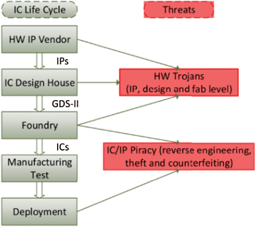
Figure 1: Threats in the IC and IP supply chain
Unlike some previous work that researched evolvable hardware [20–26] using evolutionary algorithms, this paper proposes an evolutionary algorithm called mixed-feature gene expression programming (MF-GEP) and attempts to find the original IC. The algorithm can be evolved by using a single circuit component or a group of circuit structures as the node and mixing multiple features into a single operator.
2.1.1 Composition and Attack Mechanism of Hardware Trojan
A hardware Trojan primarily consists of two components: the trigger logic and the payload. A model of the structure of a hardware Trojan is shown in Fig. 2. In this model, the payload is activated by the trigger logic through monitoring the input signal, data/control bus, register status, or a set work time. The payload is responsible for executing the attack.
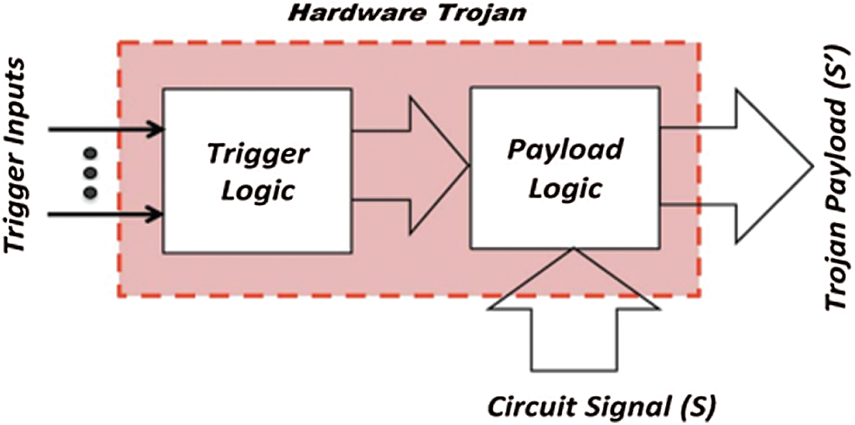
Figure 2: A hardware Trojan modifies signal S to S’ when triggered [3]
2.1.2 Destructive Detection Methods
Destructive detection methods usually use destructive reverse engineering to decapsulate an IC and obtain images of each layer, so as to reproduce and verify the trusted design of the final product [1,3,10–12]. However, the process of reverse engineering is irreversible, which means an IC can no longer be used once the intrusion process is completed, and only the information of a single IC sample is available [7–9].
Courbon et al. [10] proposed a fast-intrusive technique, which divided the IC to be tested into regions, and extracted images of each region by scanning before multiple images were stitched to reproduce the original design. Although this invasive method only works for hardware Trojans implanted by modifying functional units at the manufacturing stage, it significantly decreases the time and cost of the reverse process. Bhasin et al. [9,10] proposed the use of machine learning methods, such as support vector machine (SVM) and clustering (K-means), to identify an IC with no hardware Trojans.
The specific operation process of the SVM method is depicted in Fig. 3. This has been modified from [11].
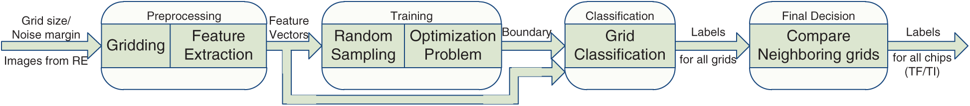
Figure 3: Hardware Trojan detection based on SVM
The author uses the golden layout of N chips to classify parameter values with grid size and noise margin dnm as input. First, the images of each layer of N chips are obtained. Then, each layer of the chips is divided into a non-overlapping grid based on the obtained images. The size and noise margin dnm of each grid are tested in the classification conditions. These grids are used to train the classifier and are subsequently classified as Trojan-free (TF) or Trojan-inserted (TI) through SVM. Finally, the classification results are used to identify whether the chip contains a Trojan.
2.1.3 Logic Test and Bypass Analysis Method
The main goal of the logic test method is to activate a hardware Trojan by applying function, structure, or random test vectors, and then compare the response result with the correct one [1,7]. However, by devising rare triggering conditions, attackers can escape traditional functional and structural tests during production testing. In addition, it is not practical to list all of the state nodes and gate circuits inside the IC. Methods based on logic testing cannot detect Trojans that do not aim at tampering with the data or functions of the original circuit, but can detect an attempt to disclose confidential information through antennas or to modify design specifications [6].
The bypass analysis method detects hardware Trojans through the parameters of an IC during normal operation, such as delay [14], power consumption [13,15], thermal radiation [16], and electromagnetic [17,18]. The method makes full use of the features of changed bypass information that are caused by additional circuits or hardware Trojans, which compensates for the lack of logic test [1,3,9,19]. However, one of the biggest challenges of this method is that bypass information analysis techniques assume a comparable “golden model,” which is often difficult to achieve in practical applications.
The concept of evolvable hardware (EHW) was initially proposed in 1993 by Hugo de Garis while at the Advanced Telecommunications Research Institute in Japan and scientists from the Swiss Federal Institute of Technology. EHW aims to make use of the reconfigurable internal structure of programmable devices, as well as the capabilities of the evolutionary algorithm in combinatorial optimization and universal search. The algorithm can help to locate the structure of the bit string combination of programmable devices for specific tasks, which obtains the hardware circuit with expected functions [21–27] through programming and configuration during the programmable periods.
For example [22], Fig. 4 illustrates the array of logic cells, and Fig. 5 shows its genotype.
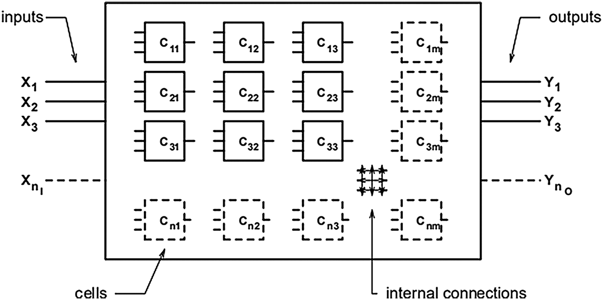
Figure 4: A digital circuit encoded within a genotype by an array of logic cells
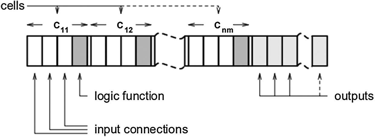
Figure 5: The genotype with respect to the rectangular array of logic cells
Xie et al. [27] proposed a two-phase EHW framework, which consists of an evolution phase based on an express tree genetic programming (ETGP) algorithm and an optimization phase based on a mining frequency digital circuit (MFDC) algorithm. It is believed that the application of GEP to EHW can rapidly generate the optimal solution of an evolutionary circuit.
Gene expression programming (GEP) [28] follows the basic steps of evolutionary computation (EC), which combines the advantages of genetic algorithms and genetic programming. Genetic material consists of two kinds of symbols: terminators and functions. A gene consists of a linear, fixed-length string of symbols and the code for expression trees, in different sizes and shapes. A chromosome can be composed of a single gene or multiple ones, decoded to map as a candidate solution for problem response.
F is the set of functions, and T is the set of terminals. GEP’s gene contains a head and a tail. The head contains symbols that represent both F and T, whereas the tail only contains T. For each problem, the length of the head h is chosen, and the length of the tail e is a function of h. The number of arguments of the function with more arguments n (also called maximum order) is evaluated by expression 1:
For example, consider a gene for the set of functions F = +, −, *, /, Q and the set of terminals T = a, b. In this case, n = 2, and if h = 10, then e = 11, and the length of the gene is 21. String 1 describes such a gene (the tail is shown in bold).
Fig. 6 shows the expression tree (ET) decoded from String 1.
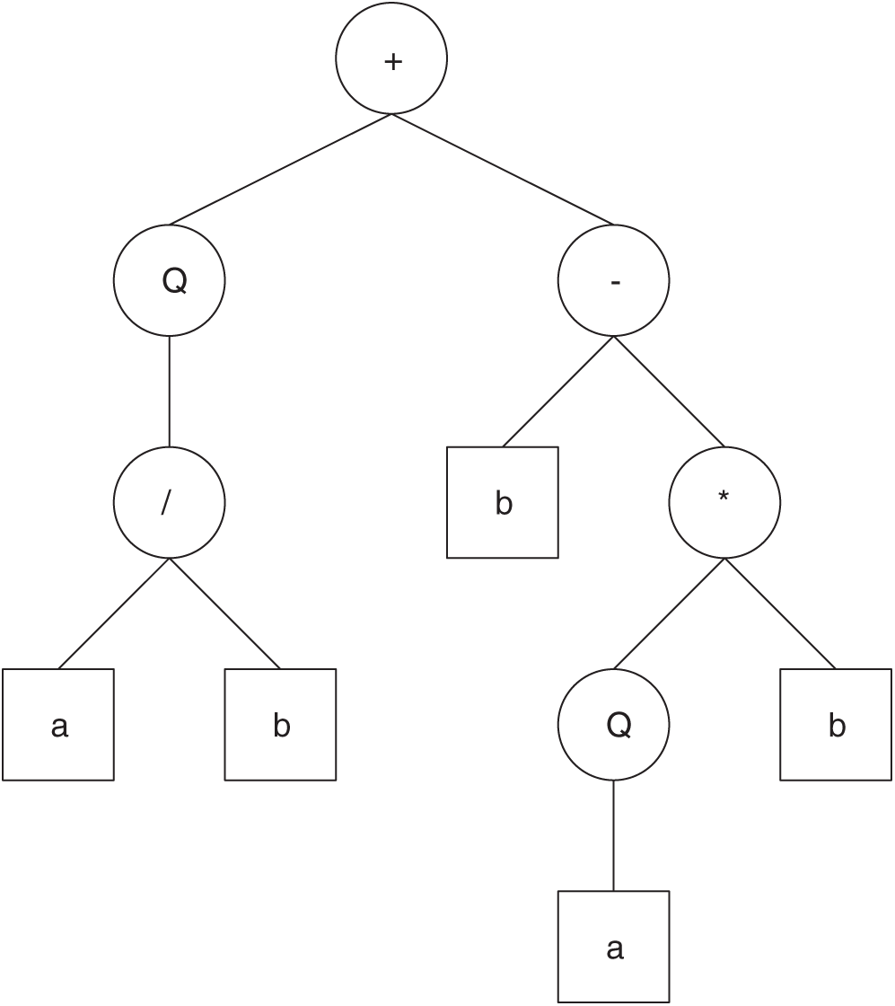
Figure 6: The expression tree decoded from String 1
The algebraic expression represented by Fig. 6 is
The redundant symbols in the tail are discarded directly. Then GEP can use fixed-length encoding to express different sizes and shapes of expression trees.
3 Using GEP to Represent Circuit
GEP has performed well in mining association rules, clustering, classification rules, time-series predictions, and sunspot predictions [29–32].
As the structure shows, GEP performs well in resolving tree-structured problems. In other words, if one circuit can be represented as a tree-shaped structure with n leaf nodes, it can be described directly with GEP. The logic circuit of the 6-in/1-out in Fig. 7a can be easily represented in an ET in Fig. 7b, which replaces the logic gate function with the logic symbol. The effective gene in GEP is shown as String 2.
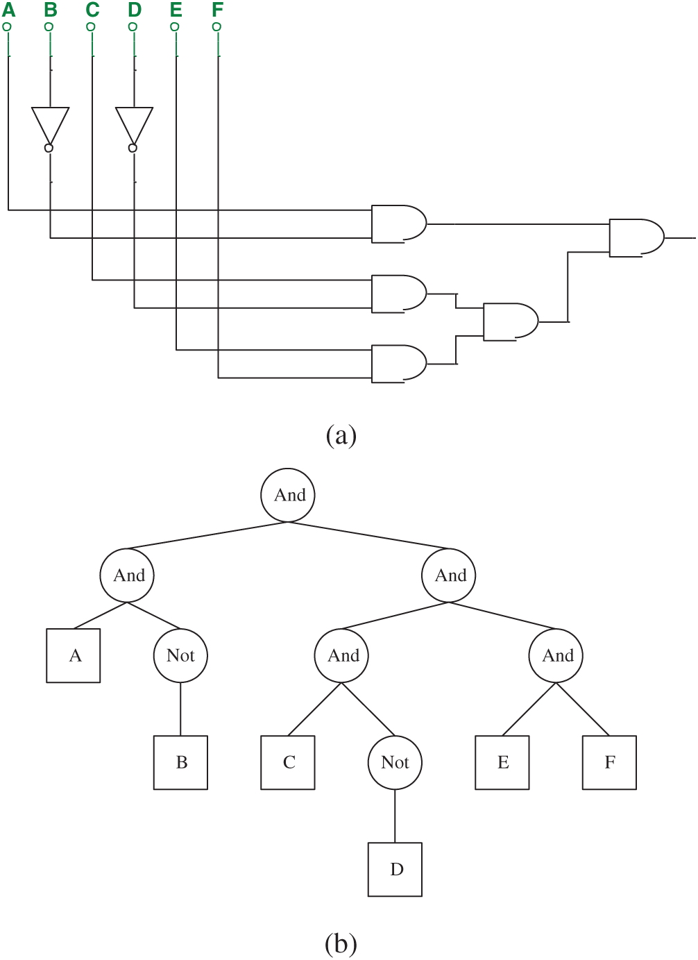
Figure 7: (a) The 6-in/1-out circuit represented by String 2 and (b) ET of the circuit shows in (a)
In GEP, uppercase letters represent operators and lowercase letters represent terminators. In this paper, however, we use the name string of the logic gate to represent logic gate, and uppercase letters to represent input parameters. The purpose of this modification is to facilitate the use of circuit simulation software.
However, if only logical values are used to represent the circuit, there would be too many isomorphic situations, For example, the circuit and its ET in Fig. 7 can be replaced with the circuit and the ET in Fig. 8.
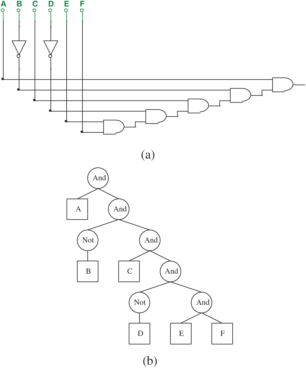
Figure 8: (a) A circuit isomorphic to Fig. 7 and (b) ET of the circuit shows in (a)
String 3 describes the corresponding effective gene of Fig. 8.
The two circuits are fully equivalent in terms of logic values, and both are shown in expression (3):
This example is only for the logic value of the circuit. A similar situation exists in terms of bypass information detection, and many different circuit structures could result from any single bypass information, which is referred to as Isomorphic in this paper.
Therefore, if a circuit is described only by logical values or a certain kind of bypass information, the circuit structure cannot be confirmed because of so much isomorphism. This paper proposes an algorithm called mixed-feature GEP (MF-GEP), which represents multiple circuit features by using the same structure in GEP. This algorithm can reduce the number of isomorphic circuits and can be used to detect hardware Trojans.
4 Formal Definition of Trojan Circuit
For a circuit R, we provide the following symbols:
Let A = Ak | k = 1,…, c be the set of all c feature values that can be tested on R.
ik = [i1, i2,…, in] is the input value vector corresponding to feature value Ak, and n is the number of input parameters of the circuit.
ok = [o1, o2,…, om] is the output value vector of input vector ik corresponding to circuit R, denoted as ok = R(ik), and m is the number of output values of R.
Ik = ik | k = 1, 2,…, d is the domain of ik, Ok = ok | k = 1, 2,…, d is the value domain of Ik.
We provide the following definitions:
Def 1
For two circuits
For
Then we call circuits R and S the same-valued isomeric circuits (SVIC) on feature Ak for input vector ik.
Def 2
For
Then we call circuits R and S the full same-valued isomeric circuits (FSVIC) on feature Ak.
Def 3
For
Then we call circuits R and S the part same-valued isomeric circuits (PSVIC) on feature Ak.
Although Strings 2 and 3 represent two different circuits, they are exactly the same in the logical value test, and both represent the circuits in expression (2). According to Def 2, Strings 2 and 3 are FSVIC in logical values. However, it is always possible to find a certain feature (such as current) that makes Strings 2 and 3 PSVIC. Therefore, Strings 2 and 3 are considered as PSVIC.
A formal definition of a Trojan circuit is as follows:
Def 4: Definition of Trojan Circuit
If the circuits R and S meet the following conditions, we call circuit R a Trojan circuit with a Trojan added to circuit S if:
1. R claims it is circuit S.
2. In fact, R is one of the PSVICs of S.
For the input domain I:
1. There are two sets of X and Y,
2. For
3. For
The smaller the scale of Y, the more difficult it is to detect the difference between R and S, and the deeper the Trojan is.
In order to make set Y in Def 4 easier to find, multiple features of the circuit were detected at the same time. Although the detection results of each feature value can build many FSVICs, different FSVICs of different features will form some PSVICs, of which the same part is possible in the real circuit.
Fig. 9 shows a Not gate designed by a triode. It is used as an example to illustrate the concept of a mixed-feature GEP algorithm.
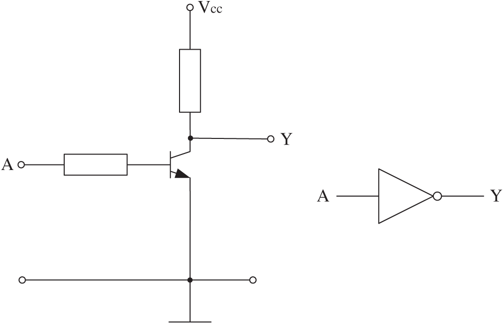
Figure 9: A Not gate designed by triode
• Feature Value 1:
In digital logic terms, the description of this circuit is:
• Feature Value 2:
In terms of voltage, the description of this circuit is:
where VSH represents the higher threshold and lower potential limit of “1” in the circuit, and VCES represents a saturation voltage drop of the triode.
• Feature Value 3:
In terms of current, the description of this circuit is:
where N is the magnification of the current.
In addition, there are a variety of other bypass information detection items, such as delay and spectrum.
With any of the above three feature values, the circuit structure cannot be determined. However, it is possible to determine the circuit structure if the three features are combined.
In GEP, an operator represents only one computation. A GEP individual only represents a description of one feature value and obtains an unlimited number of isomorphic circuits. It is impossible to determine the actual circuit structure.
The MF-GEP proposed in this paper combines the test results of multiple feature values on a circuit into a single function representation, which integrates them into a composite function, i.e., a function that represents multiple calculations at the same time. Then it evolves representations close to the original circuit by using GEP’s functional evolutionary ability.
Detection values are included in a function. The input comes from multiple feature values and the output is a vector, like the Not-gate circuit. In GEP’s ET, it is still represented by “Not,” but the implication becomes the calculation of the vector below:
where Ak (k = 1,…, n) is the input value of a type of feature detection, and Fk (Ak) (k = 1,…, n) is the result of this feature value detection corresponding to input value Ak.
However, in an electronic component, each feature value should have a different importance. So, each member of this vector should be multiplied by a weight:
For normalization, it can be specified as
For example, corresponding to this Not gate circuit, the symbol Not indicates the following meaning:
where A represents the logical value (1 or 0) by the voltage entered at point A, VA represents the input voltage of point A, and CA represents the input current of point A. [0.4, 0.3, 0.3] is the weight vector.
Therefore, when using GEP evolution, a single symbol Not also represents multiple feature values that are not associated with each other.
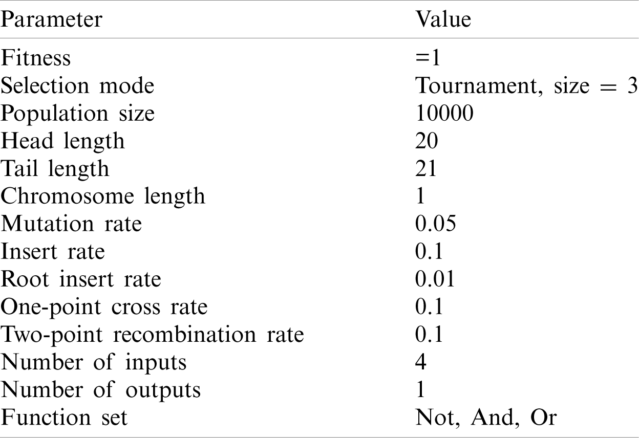
In this paper, four groups of experiments (Experiments 1–4) were designed initially. Later, in order to verify the new problems in Experiments 1–4, Experiment 5 was added. As comparison experiments, most of the parameters and fitness functions are exactly the same.
The circuit has multiple inputs and only one output. Experiment 1 used one feature, Experiments 2 and 3 used two features, Experiment 4 used three features, and Experiment 5 used two features. The three features are logical value, voltage value and current value. The GEP parameters of all the experiments are exactly the same. Tab. 1 lists the GEP parameters.
Table 1: Experiment parameters
The feature data includes logical data, voltage data, and current data, and each has its respective fitness function:
(1) Logical fitness function:
where N is the amount of test data,
a) If all
Then
Then the maximum value of F1 is 1.
b) Because of the logic value, the worst case is that every
Then
Then the minimum value of F1 is 0.
c) Suppose there are two GEP individuals, G1 and G2. For the same set of test data,
For G1, there are m
For G2, there are n
For G1, a rearrangement of (
For G2, a rearrangement of (
Because m < n, so F1(G1) < F1(G2).
Therefore, the conclusion can be drawn as follows:
i) The range of F1 is in [0, 1].
ii) With the improvement of the matching degree between the calculated value
(2) Voltage fitness function
N is the amount of test data.
The range of each
a) If all
Then
Then the maximum value of F2 is 1.
b) The worst case is that every
Then the minimum value of F2 is 0.
c) Suppose there are k (0 ≤ k < N)
Let us define EA (k,
Then,
Because
Then
When
Then
d) Suppose there are two GEP individuals, G1 and G2.
For G1, k = m, and for G2, k = n, (0 < m < n < N). The function forms of F2(G1) and F2(G2) are shown in Fig. 10.
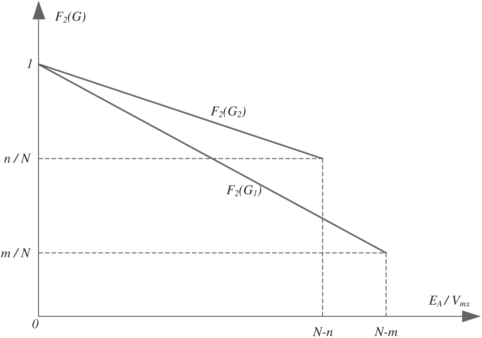
Figure 10: The function forms of F2(G1) and F2(G2)
Therefore, we can draw the conclusion that:
i) The range of F2 is in [0, 1].
ii) If individual G2 is more similar to the destination circuit than G1, there is F2(G2) > F2(G1).
(3) Current fitness function
N is the amount of test data.
(4) Individual’s fitness
According to the previous description of the algorithm, the individual’s fitness should be a combination of the three fitness functions, and therefore the individual’s fitness is defined as:
ci is the weight of corresponding Fi in final fitness. The sum of ci is 1:
If we set the weight vector
then
Fig. 11 shows a circuit that has no Trojan.
Its Boolean expression is:
The circuit makes the computation:
After several logic gates are added to the circuit of Fig. 11, it becomes a circuit with Trojan (Fig. 12). In the new circuit, Y will also get a value of 0 when (ABCD)2 = 7:
Its Boolean expression becomes:
String 4 describes the corresponding effective gene of Fig. 12.
Only a portion of the values can be tested if there are too many pins. The input value used to activate the Trojan (ABCD)2 = (0111)2 may be missed at this time. In the following experiment, the input value (0111)2 will not be provided, and the output will be determined by the evolved circuit.
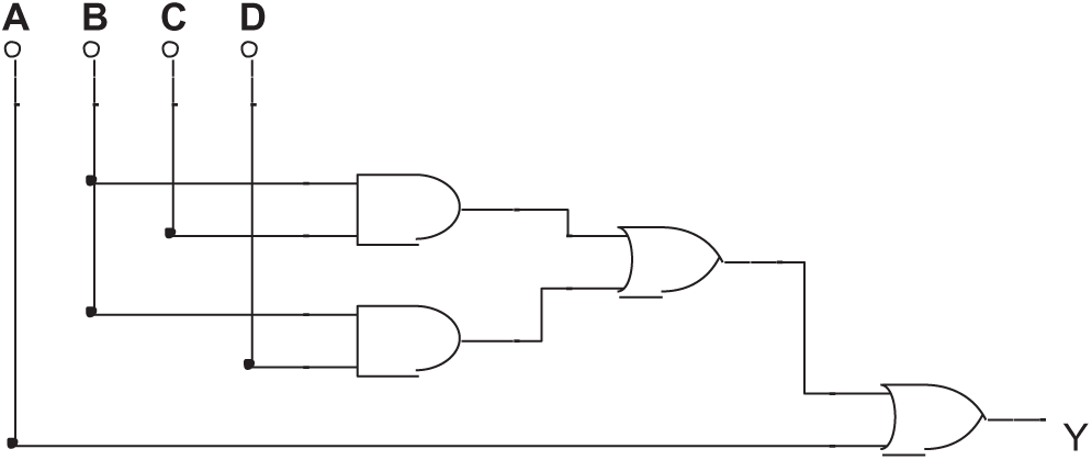
Figure 11: A circuit has no Trojan
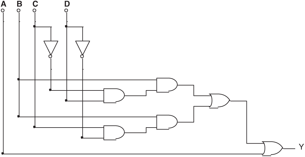
Figure 12: The circuit formed by injecting Trojan into the circuit shown in Fig. 11
Four groups of experiments were designed using different provided values and weight vectors. Considering that the logic values are first required to be correct in the circuit, the voltage and current values must be based on the correct logic values in order to make sense. The individual’s fitness is a combination of several data, in which the proportion of logical value is larger.
Tab. 2 lists the setting of Experiment 1. None of the 100 exercises were able to discover the Trojan circuit if only logical values were provided. Fig. 13 shows some typical results.
Table 2: Setting of Experiment 1
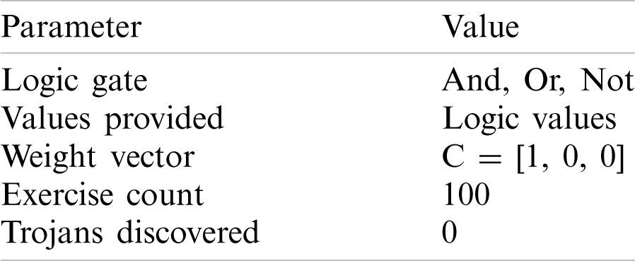
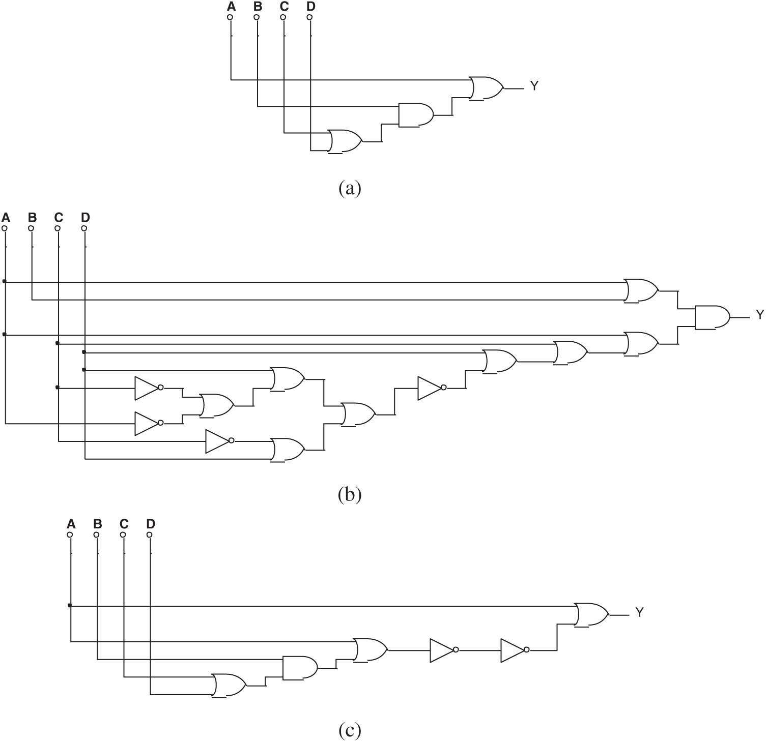
Figure 13: (a) One of the circuits evolved by mixed-feature GEP in Experiment 1, (b) Another circuit evolved by mixed-feature GEP in Experiment 1, and (c) The 3rd circuit evolved by mixed-feature GEP in Experiment 1
The simplified Boolean expression of all the circuits above is:
Tab. 3 lists the setting of Experiment 2. None of the 100 exercises were able to discover the Trojan circuit if both logical values and voltage values were provided. Fig. 14 shows some typical results.
Table 3: Setting of Experiment 2
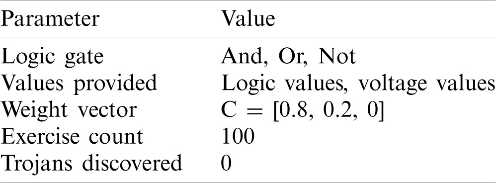
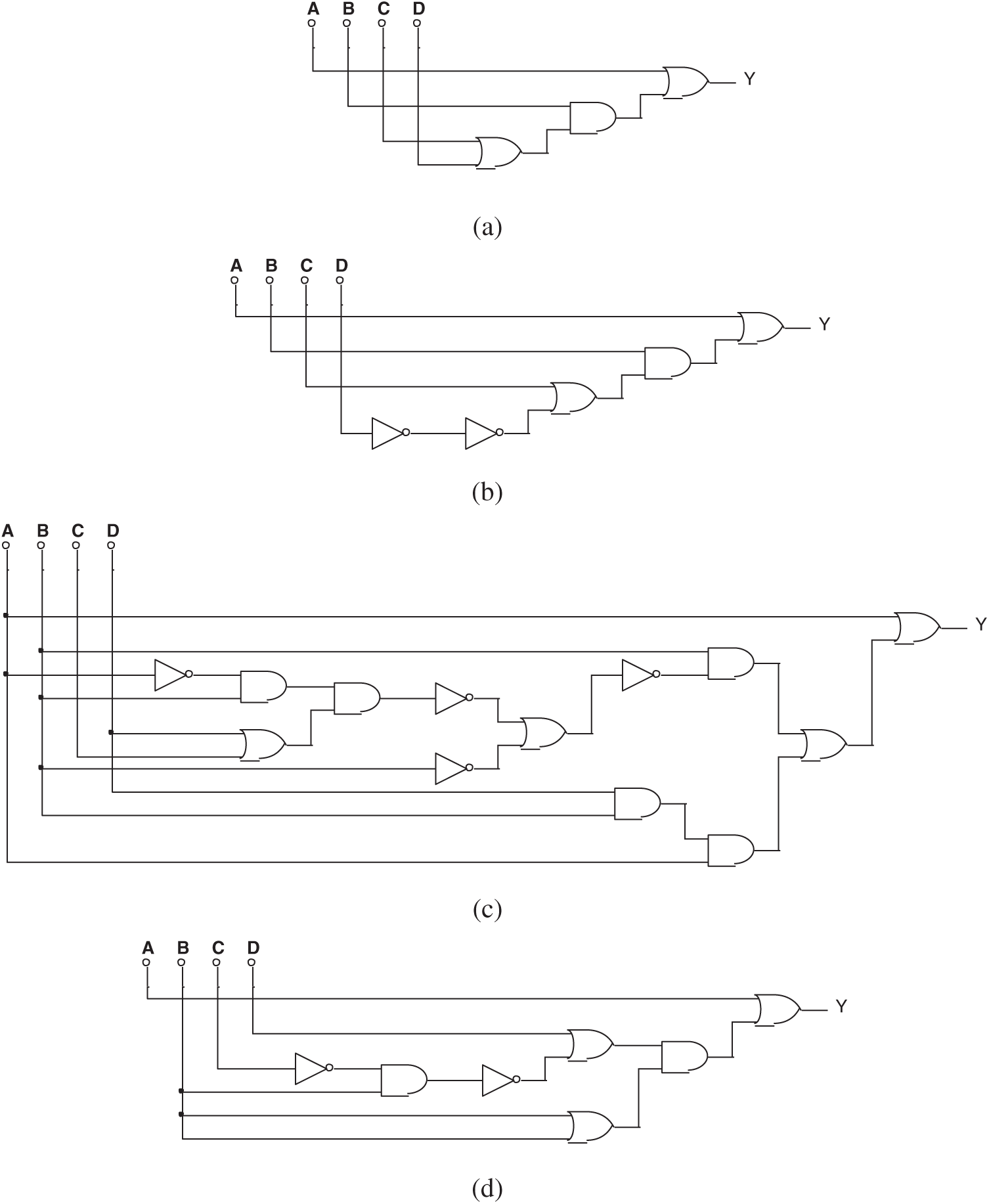
Figure 14: (a) One of the circuits evolved by mixed-feature GEP in Experiment 2, (b) Another circuit evolved by mixed-feature GEP in Experiment 2, (c) The 3rd circuit evolved by mixed-feature GEP in Experiment 2, and (d) The 4th circuit evolved by mixed-feature GEP in Experiment 2
The simplified Boolean expression of all the circuits above is:
A Trojan still cannot be found, although both the logical value and the voltage value were provided. The reason is that in digital circuits, the logic value is expressed in the form of voltage values. For example, a voltage value less than 3V is considered to be 0, and one that is greater than 3V is considered to be 1. Therefore, the choice of logical value and voltage value as feature values on this issue is as same as if only the logical value were provided.
Tab. 4 lists the setting of Experiment 3. During the 100 exercises, the Trojan circuit was discovered 72 times when logical values and voltage values were provided. Fig. 15 shows some typical results.
Table 4: Setting of Experiment 3
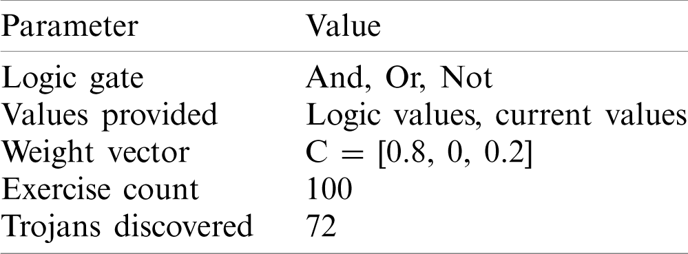
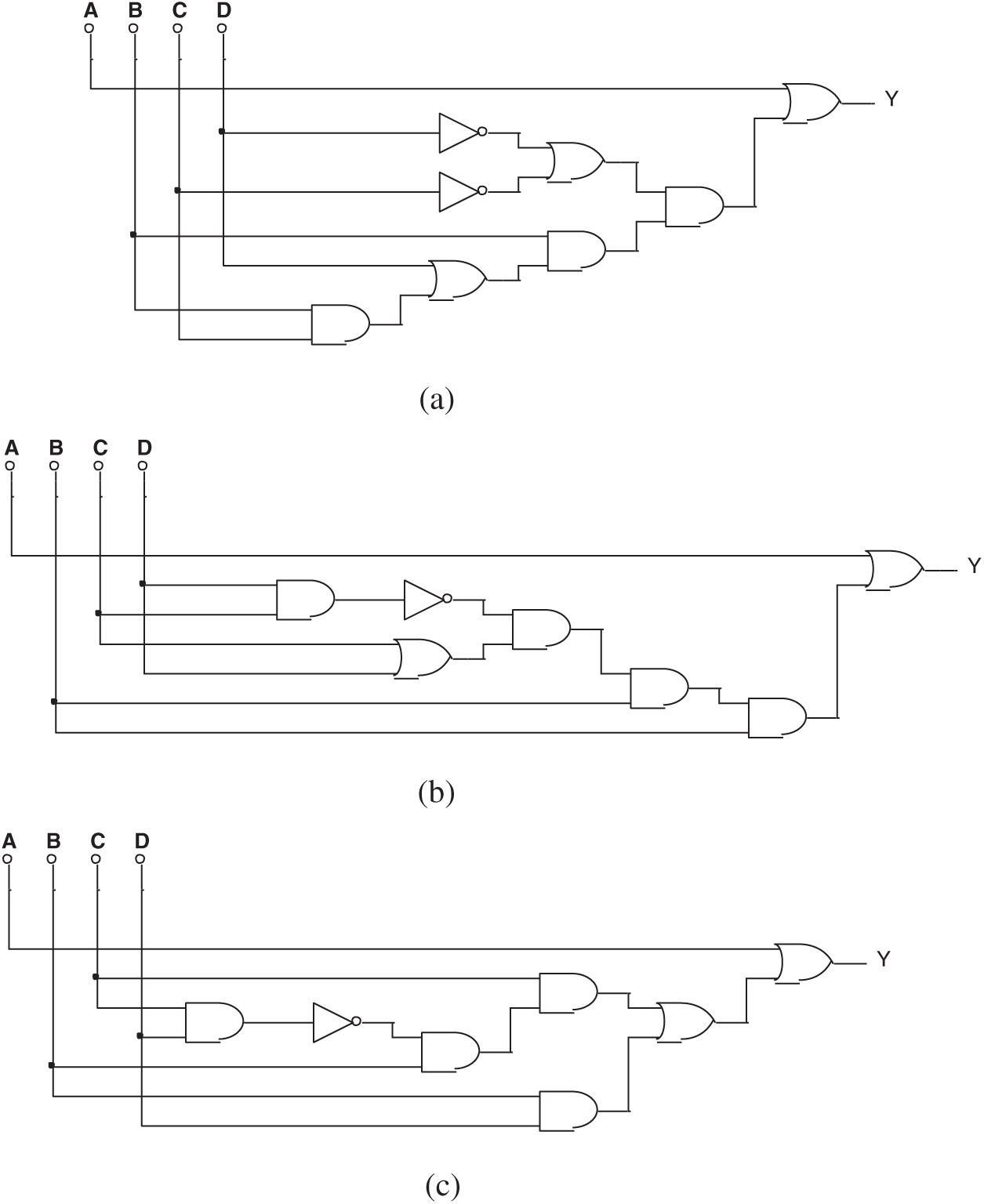
Figure 15: (a) One of the circuits evolved by mixed-feature GEP in Experiment 3, (b) Another circuit evolved by mixed-feature GEP in Experiment 3, and (c) The 3rd circuit evolved by mixed-feature GEP in Experiment 3
The simplified Boolean expression of both Figs. 15a and 15b is:
The equivalent circuit has been discovered, although the original circuit was hidden.
Fig. 15c is a failed result in finding the right circuit. Its Boolean expression is:
Tab. 5 lists the setting of experiment 4. During the 100 exercises, the Trojan circuit was discovered 67 times when all three feature values were provided. Fig. 16 shows a different result.
Table 5: Setting of Experiment 4
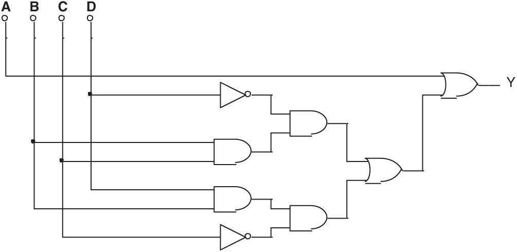
Figure 16: Typical circuit evolved by mixed-feature GEP in Experiment 4
Its simplified Boolean expression is:
A circuit equivalent to the original circuit has been found. The equivalent circuit has been discovered even though the original circuit was hidden.
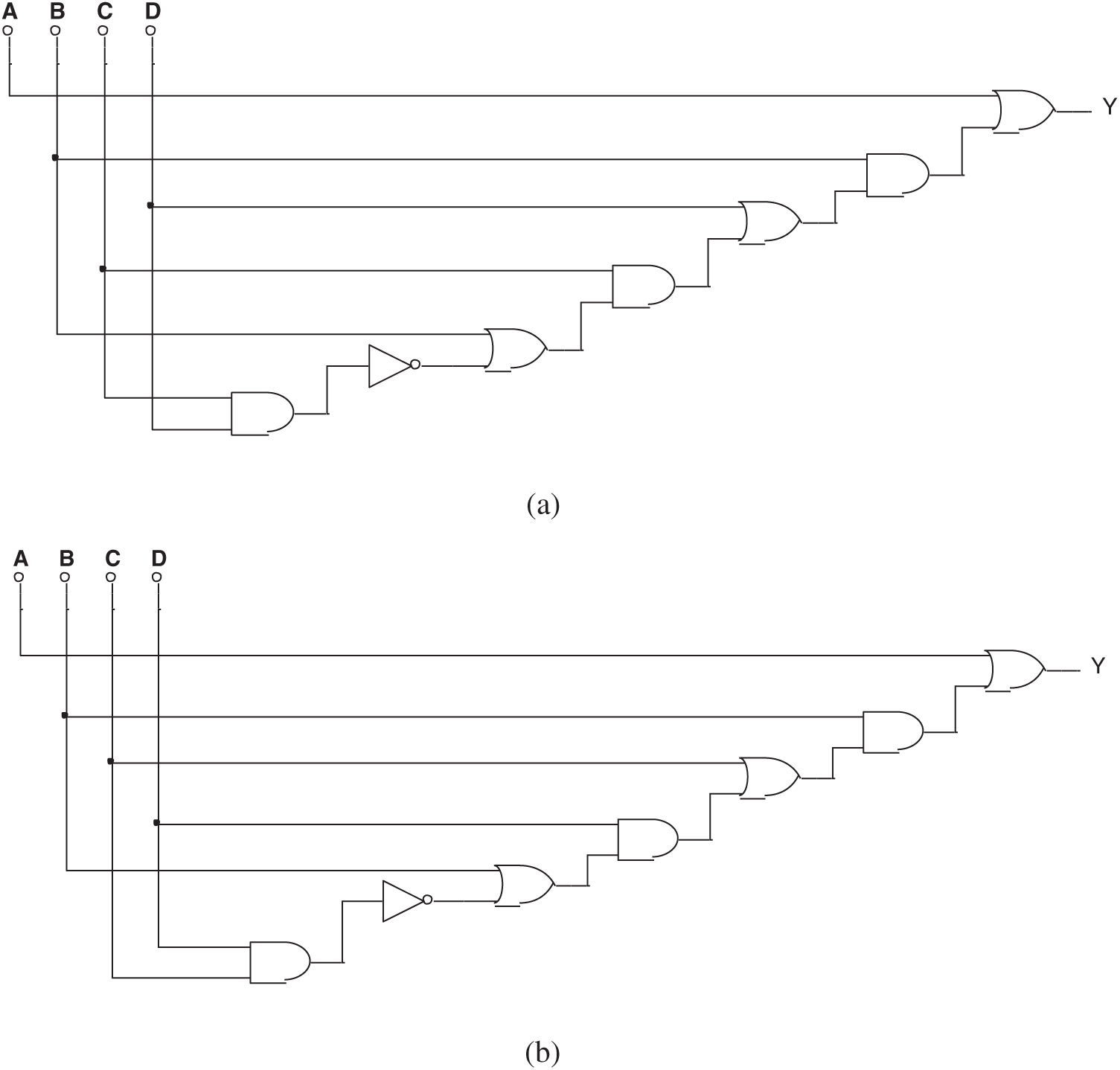
Figure 17: (a) One of the false results in Experiment 4 and (b) Another false result in Experiment 4
In this group of experiments, some wrong circuits were found by the failed evolution. As shown in Fig. 17, their Boolean expressions are:
Although three feature values were used in this group of experiments, the efficiency in discovering the Trojan was similar to that in Experiment 3, which used only two feature values. This is because the logical value itself is expressed in the form of voltage values and the three feature values are equal to the two feature values.
As discussed in Experiments 2 and 4, in digital circuits, the logical value is expressed in the form of voltage value, e.g., a voltage value less than 3V is referred to as 0, while a voltage value 3V and above is considered to be 1. Therefore, the result of using the logical value as the feature value should be similar to that of the voltage value. To verify this hypothesis, Experiment 5 is designed as a control test to Experiment 3. Tab. 6 shows the parameters and results. It differs from Experiment 3 in the replacement of the logical value by the voltage value, and the modification of the fitness function page accordingly.
Table 6: Setting of Experiment 5
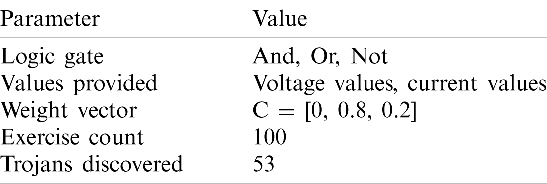
We can see that in 53 of the 100 experiments, results equivalent to Trojan circuits were obtained, but these circuits failed to make breakthrough findings in Experiments 3 and 4. However, several false circuits were found, as shown in Fig. 18. The Boolean expressions are:
Experiment 5 shows a lower probability in detecting Trojan circuits than Experiment 3. Nevertheless, the result is acceptable considering the randomness of evolutionary calculation. Results indicate that voltage data and logical value data in the mixed-feature GEP algorithm produce similar results. This verifies the hypothesis in Experiments 2 and 4 that two feature values are inter-replaceable in the algorithm if there is a simple correlation between them. Therefore, the maximization of variance between feature values helps to improve the effectiveness of the algorithm when the simple and direct correlation is uncertain.
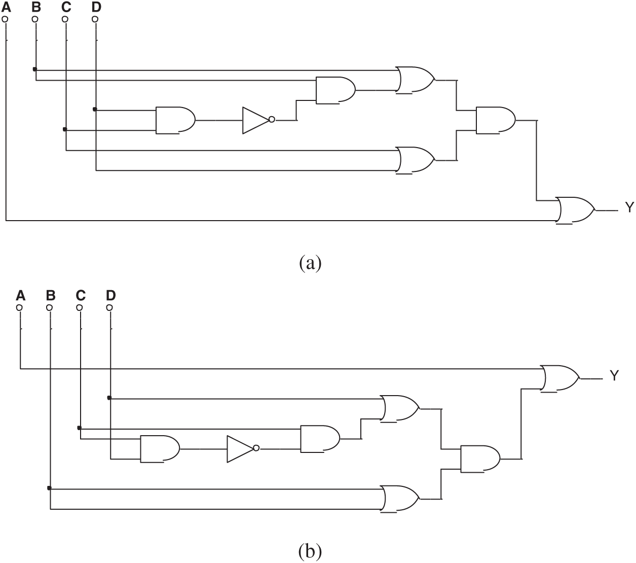
Figure 18: (a) One of the false results in Experiment 5 and (b) Another false result in Experiment 5
This paper proposes a mixed-feature GEP (MF-GEP) algorithm in which multiple feature values were fused into the same operator. There is a specific probability that Trojan circuits could be detected by MF-GEP, which automatically discovers the evolutionary power of mathematical formulas. The fewer features that are used, the higher the efficiency of the GEP evolution, but the conclusion is in wider disparity from the real circuit. At the same time, as the number of features used increases, the efficiency of GEP evolution decreases, but the conclusion drawn gets closer to the real circuit. However, if there is a direct conversion relationship between the multiple feature values used, these values can be considered as one and the accuracy of MF-GEP evolution will not be increased.
Funding Statement: This work was supported by the National Key Research and Development Program of China (Grant No. 2018YFB1502803).
Conflicts of Interest: The authors declare that they have no conflicts of interest to report regarding the present study.
1. Xiao, K., Forte, D., Jin, Y., Karri, R., Bhunia, S. et al. (2016). Hardware Trojans: Lessons learned after one decade of research. ACM Transactions on Design Automation of Electronic Systems, 22(1), 1–23. DOI 10.1145/2906147. [Google Scholar] [CrossRef]
2. Antonopoulos, A., Kapatsori, C., Makris, Y. (2017). Trusted analog/mixed-signal/RF ICs: A survey and a perspective. IEEE Design & Test, 34(6), 63–76. DOI 10.1109/MDAT.2017.2728366. [Google Scholar] [CrossRef]
3. Bhunia, S., Hsiao, M., Banga, M., Narasimhan, S. (2014). Hardware Trojan attacks: Threat analysis and countermeasures. Proceedings of the IEEE, 102(8), 1229–1247. DOI 10.1109/JPROC.2014.2334493. [Google Scholar] [CrossRef]
4. Lv, Y. Q., Zhou, Q., Cai, Y. C., Qu, G. (2014). Trusted integrated circuits: The problem and challenges. Journal of Computer Science & Technology, 29(5), 918–928. DOI 10.1007/s11390-014-1479-9. [Google Scholar] [CrossRef]
5. Tehranipoor, M., Wang, C. (2012). Introduction to hardware security and trust. USA: Springer Publishing Company. [Google Scholar]
6. Wang, X., Tehranipoor, M., Plusquellic, J. (2008). Detecting malicious inclusions in secure hardware: Challenges and solutions. Proceedings of the 2008 IEEE International Workshop on Hardware-Oriented Security and Trust, pp. 15–19. Anaheim, CA, USA. [Google Scholar]
7. Tehranipoor, M., Koushanfar, F. (2010). A survey of hardware Trojan taxonomy and detection. IEEE Design and Test of Computers, 27(1), 10–25. DOI 10.1109/MDT.2010.7. [Google Scholar] [CrossRef]
8. Zhao, J. F., Shi, G. (2017). A survey on the studies of hardware Trojan. Journal of Cyber Security, 2(1), 74–90. DOI 10.19363/j.cnki.cn10-1380/tn.2017.01.006. [Google Scholar] [CrossRef]
9. Bhasin, S., Regazzoni, F. (2015). A survey on hardware Trojan detection techniques. Proceedings of the 2015 IEEE International Symposium on Circuits and Systems, pp. 2021–2024. Lisbon, Portugal. [Google Scholar]
10. Courbon, F., Loubet-Moundi, P., Fournier, J. J. A., Tria, A. (2015). SEMBA: A SEM based acquisition technique for fast invasive hardware Trojan detection. Proceedings of the 2015 European Conference on Circuit Theory and Design, pp. 1–4. Trondheim, Norway. [Google Scholar]
11. Bao, C. X., Forte, D., Srivastava, A. (2014). On the application of one-class SVM to reverse engineering-based hardware Trojan detection. Proceedings of the 15th International Symposium on Quality Electronic Design, pp. 47–54. Santa Clara, CA, USA. [Google Scholar]
12. Bao, C. X., Forte, D., Srivastava, A. (2015). On reverse engineering-based hardware Trojan detection. IEEE Transactions on Computer-Aided Design of Integrated Circuits and Systems, 35(1), 49–57. DOI 10.1109/TCAD.2015.2488495. [Google Scholar] [CrossRef]
13. Agrawal, D., Baktir, S., Karakoyunlu, D., Rohatgi, P., Sunar, B. (2007). Trojan detection using IC fingerprinting. Proceedings of the 2007 IEEE Symposium on Security and Piracy, pp. 296–310. Berkeley, CA, USA. [Google Scholar]
14. Xiao, K., Zhang, X., Tehranipoor, M. (2013). A clock sweeping technique for detecting hardware Trojans impacting circuits delay. IEEE Design & Test, 30(2), 26–34. DOI 10.1109/MDAT.2013.2249555. [Google Scholar] [CrossRef]
15. Aarestad, J., Acharyya, D., Rad, R., Plusquellic, J. (2010). Detecting Trojans through leakage current analysis using multiple supply pad IDDQs. IEEE Transactions on Information Forensics and Security, 5(4), 893–904. DOI 10.1109/TIFS.2010.2061228. [Google Scholar] [CrossRef]
16. Nowroz, A. N., Hu, K., Koushanfar, F., Reda, S. (2014). Novel techniques for high-sensitivity hardware Trojan detection using thermal and power maps. IEEE Transactions on Computer—Aided Design of Integrated Circuits and Systems, 33(12), 1792–1805. DOI 10.1109/TCAD.2014.2354293. [Google Scholar] [CrossRef]
17. Zhou, B. Y., Adato, R., Zangeneh, M., Yang, T. Y., Uyar, A. et al. (2015). Detecting hardware Trojans using backside optical imaging of embedded watermarks. Proceedings of the 2015 52nd ACM/EDAC/IEEE Design Automation Conference, pp. 1–6. San Francisco, CA, USA. [Google Scholar]
18. He, J., Zhao, Y., Guo, X., Jin, Y. (2017). Hardware Trojan detection through chip-free electromagnetic side-channel statistical analysis. IEEE Transactions on Very Large Scale Integration Systems, 25(10), 2939–2948. DOI 10.1109/TVLSI.2017.2727985. [Google Scholar] [CrossRef]
19. Jacob, N., Merli, D., Heyszl, J., Sigl, G. (2014). Hardware trojans: Current challenges and approaches. IET Computers & Digital Techniques, 8(6), 264–273. DOI 10.1049/iet-cdt.2014.0039. [Google Scholar] [CrossRef]
20. Higuchi, T., Murakawa, M., Iwata, M., Kajitani, I., Liu, W. X. et al. (1997). Evolvable hardware at function level. Proceedings of the 1997 IEEE International Conference on Evolutionary Computation, pp. 187–192. Indianapolis, IN, USA. [Google Scholar]
21. Higuchi, T., Iwata, M., Kajitani, I., Iba, H., Hirao, Y. et al. (1996). Evolvable hardware and its application to pattern recognition and fault-tolerant systems. Towards evolvable hardware, pp. 118–135. Berlin: Springer Verlag. [Google Scholar]
22. Vassilev, V., Job, D., Miller, J. (2000). Towards the automatic design of more efficient digital circuits. Proceedings of the 2nd NASA/DOD Workshop on Evolvable Hardware, pp. 151–160. Palo Alto, CA, USA. [Google Scholar]
23. Timothy, G. W., Peter, J. B. (2002). Towards development in evolvable hardware. Proceedings of the 3rd NASA/DOD Workshop on Evolvable Hardware, pp. 241–250, Pasadena. [Google Scholar]
24. Erbo, M., Rossi, R., Liberali, V., Tettamanzi, A. G. B. (2001). Digital filter design through simulated evolution. Proceedings of the European Conference on Circuit Theory and Design, pp. 389–393. Espoo, Finland. [Google Scholar]
25. Hemmi, H., Mizoguchi, J., Shimohara, K. (1994). Development and evolution of hardware behaviors. Towards Evolvable Hardware, pp. 250–265. Berlin: Springer Verlag. [Google Scholar]
26. Hounsell, B., Arslan, T. (2000). A novel evolvable hardware framework for the evolution of high performance digital circuits. Proceedings of the Genetic and Evolutionary Computation Conference, pp. 525–529. Las Vegas, Nevada, USA. [Google Scholar]
27. Xie, F. J., Tang, C. J., Yuan, C. A., Zuo, J., Cheng, A. L. (2005). An algorithm of evolution and optimization for evolvable hardware. Journal of Computer—Aided Design and Computer Graphics, 17(17), 1415–1420. DOI 10.3321/j.issn:1003-9775.2005.07.006. [Google Scholar] [CrossRef]
28. Ferreira, C. (2001). Gene expression programming: A new adaptive algorithm for solving problems. Complex Systems, 13(2), 87–129. DOI 10.1007/3-540-32849-1. [Google Scholar] [CrossRef]
29. Ferreira, C. (2002). Gene expression programming: Mathematical modeling by an artificial intelligence. USA: Springer Verlag. [Google Scholar]
30. Zuo, J., Tang, C. J., Zhang, T. Q. (2002). Mining predicate association rule by gene expression programming. Proceedings of the 3rd International Conference for Web-Age Information Management, pp. 281–294. Beijing, China. [Google Scholar]
31. Zuo, J., Tang, C. J., Li, C., Yuan, C. A., Chen, A. L. (2004). Time series prediction based on gene expression programming. Proceedings of the 5th International Conference for Web-Age Information Management, pp. 55–64. Dalian, China. [Google Scholar]
32. Zhou, C., Xiao, W., Tirpak, T. M., Nelson, P. C. (2003). Evolution accurate and compact classification rules with gene expression programming. IEEE Transaction on Evolutionary Computation, 7(6), 519–531. DOI 10.1109/TEVC.2003.819261. [Google Scholar] [CrossRef]
 | This work is licensed under a Creative Commons Attribution 4.0 International License, which permits unrestricted use, distribution, and reproduction in any medium, provided the original work is properly cited. |