| Computer Modeling in Engineering & Sciences |
DOI: 10.32604/cmes.2022.016086
ARTICLE
A Chopper Negative-R Delta-Sigma ADC for Audio MEMS Sensors
1College of Computer Engineering and Sciences, Prince Sattam bin Abdulaziz University, Alkharj, 11942, Saudi Arabia
2Université Paris-Saclay, CentraleSupélec, CNRS, Laboratory de Génie Electrique et Electronique de Paris, Gif-sur-Yvette, 91192, France
3Sorbonne Université, CNRS, Lab. de Génie Electrique et Electronique de Paris, Paris, 75252, France
*Corresponding Author: Jamel Nebhen. Email: J.nebhen@psau.edu.sa
Received: 5 February 2021; Accepted: 8 September 2021
Abstract: This paper presents a proposed low-noise and high-sensitivity Internet of Thing (IoT) system based on an M&NEMS microphone. The IoT device consists of an M&NEMS resistive accelerometer associated with an electronic readout circuit, which is a silicon nanowire and a Continuous-Time (CT) Δ Σ ADC. The first integrator of the Δ Σ ADC is based on a positive feedback DC-gain enhancement two-stage amplifier due to its high linearity and low-noise operations. To mitigate both the offset and 1/f noise, a suggested delay-time chopper negative-R stabilization technique is applied around the first integrator. A 65-nm CMOS process implements the CT Δ Σ ADC. The supply voltage of the CMOS circuit is 1.2-V while 0.96-mW is the power consumption and 0.1-mm2 is the silicon area. The M&NEMS microphone and Δ Σ ADC complete circuit are fabricated and measured. Over a working frequency bandwidth of 20-kHz, the measurement results of the proposed IoT system reach a signal to noise ratio (SNR) of 102.8-dB. Moreover, it has a measured dynamic range (DR) of 108-dB and a measured signal to noise and distortion ratio (SNDR) of 101.3-dB.
Keywords: M&NEMS sensor; Δ Σ; ADC; chopper negative-R; IoT; 1/f noise; SNR
In recent years, a new system called the Internet of Things (IoT) has increasingly gained ground. IoT depicts a large network of interconnected sensors and objects that are uniquely addressable, built on common networking protocols, the subject of which is the Internet. The IoT system is focused on the pervasive existence of objects surrounding individuals capable of weighing, deducting, recognizing, and even altering their environment. It is based on intelligent and interconnected nodes within a complex and extensive network infrastructure [1]. It is typically defined by small real-world objects, widely dispersed, with minimal storage and processing power, suggesting reliability, efficiency, protection, and privacy issues. It is driven by recent developments in different devices and technologies for communication. This refers to complicated devices like cell phones and basic items like clocks, thermostats, clothing, etc., that are used every day [2]. These objects can connect and interact with their neighborhood, operating as sensors or actuators. Wireless Sensor Networks (WSNs) are self-configured, infrastructure-free wireless networks that monitor physical or environmental conditions such as sound, temperature, vibration, motion, pressure, or pollutants and cooperatively pass their data through the network to a central location or sink where the data can be observed and analyzed. A wireless sensor network typically consists of hundreds of thousands of sensor nodes [3]. Radio signals allow the sensor nodes to communicate with one another. Sensing and computing devices, radio transceivers, and power components are all included in a wireless sensor node [4]. Sensors and actuators are the key building blocks of the IoT system. They monitor the state of their environment; obtain information on temperature, movement, position, etc. They form a network usually composed of a potentially large number of nodes. These sensors have to face many communication problems such as security and confidentiality, mobility, short-range, reliability, robustness, scalability, and resources.
Micro-Electro-Mechanical Systems (MEMS) circuits integrate sensors, mechanical elements, actuators, and electronic circuits in the same silicon substrate. Nowadays, there is an immensely high demand for the MEMS market. Therefore, audio applications commonly use MEMS microphones owing to their fundamental requirements, which consist of small size, low-power consumption, high sound quality, high sensitivity, and reliability. For the MEMS microphone, the main goal of the design and optimization of its electronic circuits is to improve the audio performances. Among these audio performances, it is necessary to increase the signal-to-noise ratio (SNR), the total harmonic distortion (THD), the dynamic range (DR), and the low-power consumption. Based on their output, two categories of MEMS microphones exist namely the analog MEMS microphone and the digital MEMS microphone. The CMOS chip of the digital MEMS microphone integrates an Analog to Digital Converter (ADC) in the objective to generate a digital output. As a result, the complete circuit is easily integrated with modern digital systems. Due to its high resolution, inherent linearity, and wide dynamic range; the audio application uses Delta-Sigma (Δ Σ) ADC [5]. The Δ Σ ADC sampling frequency is very high compared to the Nyquist rate being an oversampled converter. Due to their high resolution, applications working in the low to medium bandwidth extensively use Δ Σ ADCs [6], such as MEMS microphone [7], audio systems [8], sensing applications [9] and wireless communications [10]. Recent trends in the mobile microphone market are targeting 70 dB A-weighted signal-to-noise ratio (SNR) at 94 dB sound pressure level (SPL) and higher acoustic overload points. In the readout circuit of microphones, an ADC having a dynamic range (DR) far above 100 dB A-weighted can meet this condition. In addition, a high value of signal-to-noise and distortion ratio (SNDR) is also preferred so as to preserve the fidelity of acoustic signal source at high sound pressure levels above 94 dB SPL. However, to reduce the power consumption of digital circuits including application processor in mobile devices, the supply voltage is getting lower, and thus interface circuits such as the ADC having high DR and SNR should also be designed to operate at a low supply voltage.
Audio systems have traditionally used multibit Δ Σ ADC often based on a switched capacitor circuit [11]. Continuous-time (CT) solutions, on the other hand, are becoming extremely prevalent for low bandwidth ADC applications. ADC is commonly used for audio applications because of its high SNR, reduced power consumption, and high resolution [12]. In the last decade, deep-submicron CMOS technology has become a solution for continuous scaling, low cost, and low power devices. The bias voltage, however, becomes very low, under one-Volt, reducing the signal swing as low as analog circuit supply voltage limits (i.e., CT filters). The ADC depicts a very important interface separating the analog and the digital circuit. When designing a CMOS system, the ADC circuit and the CMOS digital circuit are implemented with the same CMOS process. Therefore, the reduction of the ADC’s power consumption is inevitable. The main goal is to decrease the ADC’s supply voltage. However, the drawback of this technique is the degradation of ADC performance. If the signal swing of the system is decreased, its noise floor must be decreased to keep the same circuit dynamic range. Therefore, reducing the supply voltage for high-resolution audio systems leads to a serious distortion problem.
High performance and high-resolution audio systems are based on a Δ Σ ADC owing to its high linearity [12]. This characteristic is obtained by integrating the oversampling technique with the inherent single-bit linear quantizer. Non-idealities of building blocks, however, strongly influence its efficiency. If a nanometer CMOS technique is used, the performance seems even worse. The restriction of their headroom function induced by the reduction of the bias voltage affects the working devices [13]. Moreover, the figure-of-merit (FOM) of the implemented circuit is affected. Furthermore, the Δ Σ ADC designed with this technology needs a low SNR and low-noise floor with the same dynamic range. The output is then impacted and the energy consumption is increased [14]. The most critical parameter for designing a Δ Σ ADC with high resolution is to increasing its linearity.
The goal of this paper is to implement an IoT device consisting of an M&NEMS microphone and an ADC that has a high peak-SNR, high peak SNDR, and high Schreier’s FOM. The CMOS architecture of a Δ Σ ADC is particularly chosen. Besides, proposed electronic circuits to improve performances are designed and discussed. We have adopted the Low-Energy Adaptive Clustering Hierarchy (LEACH) as the communication protocol of the data transmission among sensor nodes. LEACH includes randomized rotation of the high-energy cluster-head position such that it rotates among the various sensors in order to not drain the battery of a single sensor. LEACH performs local data fusion to “compress” the amount of data being sent from the clusters to the base station, further reducing energy dissipation and enhancing system lifetime. The whole IoT device is designed and manufactured in a 65-nm CMOS process. Measurement results are analyzed and compared with the state-of-the-art. The paper sections are arranged as follows: a description of the manufactured M&NEMS microphone is presented in Section 2. Section 3 gives the specifics of the Δ Σ ADC implementation. Section 4 explains the suggested chopper negative-R solution for reducing the first integrator’s flicker noise. The measurement results and analysis of the proposed IoT system are described in Section 5. Finally, Section 6 becomes to conclude our proposed IoT system.
To detect acoustic vibrations, nanowire microphones use piezo-resistivity. They reflect the latest generation and the newest technology of the M&NEMS piezoresistive sensors that have already been developed in the CEA-Leti. The strength of this proposed M&NEMS piezoresistive sensor is that silicon-based nanowires are used to produce an electrical output response [15]. The silicon nanowire microphone combines an integrated mechanical system of components in movement, like other M&NEMS sensors. To generate a high nanowires mechanical stress, the architecture of this mechanical component is carefully established. The development of the M&NEMS resistive sensor is carried out in the cleanroom of the CEA-Leti, as defined in Fig. 1. Two stacked wafers are part of the microphone, as shown in Fig. 2. The wafer on the top has vents for outlets. These events represent acoustic guides through which the incident acoustic wave circulates. The bottom wafer contains electrical input-output contacts, microstructures that bring silicon nanowires under tension-compression, and inlet vents for access to the nanowire resistors. The proposed M&NEMS piezoresistive sensor depicts an invention done by CEA-Leti [16]. A diaphragm located between the top wafer and the bottom wafer represents the M&NEMS microphone. For M&NEMS implementation, the top and the bottom wafer are used, respectively, as a cap and a base. To achieve effective sound pressure amplification and a good static pressure’s equalization, the acoustic sound vents and the two wafers will be etched. The microphone acts as follows; when a disturbance appears, the actuation of the pressure spread through the acoustic inlet vents in the bottom wafer and moves to the diaphragm. The actuation of the pressure then varies in proportion to the differential pressure in the top wafer between the inlet and outlet vents. It is conceivable to multiply the inlet vents, the outlet vents, and the diaphragms to build an efficient M&NEMS piezoresistive sensor.

Figure 1: SEM photograph of the M&NEM based nanowire sensor

Figure 2: Cross-section of the M&NEMS microphone (a) Sensing elements and acoustic configuration (b) Nanowire position is indicated by the white arrows and in-plane microstructures displacement
A sound wave pressure attacks the inlet vents. The piezoresistive effect causes the silicon nanowire resistance to be varied according to the applied stress. A piezoresistive phenomenon is present in the doped crystalline silicon. Consequently, in M&NEMS sensors, this phenomenon is widely used as a detection process. The implementation of piezoresistors into silicon membranes enables the microphone to detect the overall sound pressure by generating a piezoresistive effect. By the selective deposition technique of the doped silicon substrate, piezo resistors may be embedded into silicon membranes. Besides, the selective doping approach of the silicon membrane may be implemented in the fabrication or diffusion process [17]. Therefore, since the detected stress is spread over the complete surface of the membrane, the optimization of the M&NEMS sensor reflects to optimize the stress of the internal piezo resistors. Piezo resistors must be mounted in regions of the highest stress [18]. Furthermore, the thickness of the microphone membrane and the thickness of the piezoresistor must have a significant proportion [19]. Consequently, in the center of the membrane side, maximum tensional longitudinal stress appears. Moreover, in the center of the M&NEMS sensor membrane, there is another maximum compressional stress.
If acceleration is sensed, then a rotational movement acts automatically on the seismic mass. By respecting the rotational axis, this rotational movement is achieved. The resulting inertial force is then used to create longitudinal or tension stress in the nanogage section. The nanogauge stress makes the creation of a resistance change proportional to the inertial force due to the piezoresistive effect. A lever effect factor amplifies the resistance difference. The lever effect is the resulting distance separating the axis of rotation and the seismic mass center, divided by the resulting distance separating the rotation axis and the nanogauge position. In addition, by having trenches and a boss, the special membrane features will create stress concentration regions [20]. A p-n junction between the interfaces of membrane-piezoresistors is then formed when the piezoresistors are embedded into the membrane. This junction produces a current for leakage. The piezoresistor bias current is higher at room temperature than the leakage current, which can be ignored. The leakage current also increases if the temperature increases, and it can affect the sensor response [21].
The architecture of the suspended nanowires is adopted to design the M&NEMS resistive accelerometer. The p-type piezoresistive effect of silicon nanowires was studied [22]. Compared to bulk silicon, the piezoresistive effect greatly improves at the nanoscale. Hence, for more robust MEMS sensors, silicon nanowires are very effective. 1.5 × 1.5 × 0.6 mm3 is the average size of the M&NEMS piezoresistive sensor. Four microbeams depict the M&NEMS sensor. They are mounted between the inlet and outlet vents. The M&NEMS microbeam shifts rotationally according to the applied stress.
The proposed concept uses a membrane able to move in the plane of the substrate and not out of plane. The first advantage of the proposed concept is the decorrelation of the acoustic part and the detection part, which enables to optimize them independently. The second advantage is the same fabrication process for both microphones and accelerometers, which enables either to co-integrate these two sensors on the same chip or to use the same technological platform for these two components. The MEMS fabrication is carried out at CEA-LETI clean room with typical micro-electronic process. MEMS microphone exhibits 30 dB of Equivalent Input Noise (EIN) with a resolution of 95 nV/bits. Analytical calculation shows that 74 dB SNR (Signal to Noise Ratio) could be achieved with biasing current of 100 μA and readout circuit featuring 6 nV/
3 Implementation of the Δ Σ ADC Circuit
Audio applications including hearing aids implant involve large dynamic range and low power consumption. Acoustic vibration lower than 30 dB SPL (Sound Pressure Level) must be resolved while sound pressure over 110 dB SPL must not generate harmonic distortion. Commercially available digital output MEMS microphones feature 30 dB SPL of equivalent input referred noise, power consumption lies in the mA range with supply voltage of 2.5 V. The proposed M&NEMS microphone targets input referred noise of 5 dB SPL lower than commonly used MEMS microphones. For high sensitivity of the microphone, the system was designed with a tradeoff between, noise performance, and power consumption where an optimal repartition of the current budget between the sensor bias and the analog front-end building blocks has to be achieved.
Two topologies are used to implement the Δ Σ ADC. The first one is the distributed feedforward topology. The second one is a distributed feedback topology. The signal in the output of the sensor is connected to the loop filter of the feedback topology. Therefore, large swings are introduced in the integrator by this input component. Therefore, the amplifier needs high linearity. This problem is very hard in low-voltage electronic architecture. The two-voltage components of the CMOS transistor, which are the threshold voltage and the drain to the source voltage, do not meet the same external bias voltage. On the other hand, a specific behavior is generated by feedforward topology [23]. In this topology, the shaped quantization noise depicts the only available noise component in the loop filter input. The direct feeding of the integrator’s outputs and the input signal to the quantizer allows achieving this main advantage. Moreover, the quantizer output is connected to the input of the first integrator. Cascaded continuous time integrator feed-forward sigma delta seems to be the best ADC topology to accomplish the involved trade off. First, continuous time integrator provides intrinsic anti-aliasing filtering saving filter stage power consumption; second, feed-forward implementation reduces integrators output swing requirement making amplifier design easier; third, unlike switched capacitor integrator, amplifier settling time requirement is relaxed, so as the saved power budget can be allocated to input stage in favor of noise performance.
The voltage fluctuations into the integrators are widely mitigated if there is no signal coming from the sensor. Therefore, both the linearity and the slew rate of the amplifier are improved, while a reduction of its current consumption. Thus, the feedforward topology is a suitable solution to mitigate both the ADC power consumption and noise. The ADC for quantization uses a single-bit quantizer because any complex element matching circuit does not require by the DAC and the ADC circuit is inherently linear. Moreover, owing to the configuration of only two DACs and one comparator without a calibration circuit, the total power consumption and the overall silicon area of the DAC and digital circuit are much lower than the multibit quantizer [24]. On the other hand, the noise specification for quantization requires the oversampling ratio and the Δ Σ ADC order to be defined. To minimize the amplifier’s power consumption, the Δ Σ ADC’s thermal noise must be widely mitigated.
Audio applications have a relatively small bandwidth (B from 20-Hz to 20-kHz). As a result, Δ Σ ADC is particularly suited for this bandwidth. The Δ Σ ADC solution can achieve a large oversampling ratio
where M, N, and L values can be chosen to achieve the target high SNR value. The Δ Σ ADC is simpler if it has an order of two with N = 1 [26]. However, in this case, M values should be high, which requires the integrators opamps with high slew-rate and high gain bandwidth. Therefore, the Δ Σ ADC is affected by high power consumption. Although, if the Δ Σ ADC has the fourth-order filtering with N = 1, then the requirements for each integrator will be more relaxed. The non-dominant quantization noise can be set by 10-dB under the overall Δ Σ ADC noise. The fourth-order integrator topology is chosen for the order of the Δ Σ ADC, as well as the oversampling M of 77 is set. The ADC has a 3.072-MHz sampling frequency and a 20-kHz signal bandwidth. The ADC coefficients are ai for the integrator coefficient, ki for the feedforward coefficient, and Voi for the output of the integrator, with i = 1 … 4, as shown in Fig. 3 [27]. They are derived from the Δ Σ ADC presented in [28]. In the objective of achieving high SNR with good loop stability, a behavioral simulation is used to optimize these coefficients.

Figure 3: Circuit diagram of the CT Δ Σ ADC with the integrator coefficient ai, the feedforward coefficient for ki, and the output of the integrator Voi
In this design, the DAC placed in the feedback is based on a non-return-to-zero (NRZ) pulse. Compared with the architecture of a return-to-zero (RZ) pulse and a half-delayed return-to-zero (HRZ) pulse, clock jitter does not affect the sensitivity of the NRZ pulse [29]. The input pulse is constant over the complete clock cycle. Therefore, the NRZ DAC pulse relaxes the first integrator slew rate. Moreover, the first integrator has low power consumption. Fig. 4 describes the complete circuit of the Δ Σ ADC. Each integrator is based on a closed-loop active-RC filter architecture. This architecture allows increasing the linearity and parasitic insensitivity of the integrator. The virtual ground of the active-RC filter maintains the amplifier input range requirement is relaxed. Therefore, when working at a low voltage level, the closed-loop active-RC filter is appropriate.

Figure 4: Circuit of the proposed CT Δ Σ ADC
The SNR of the Δ Σ ADC is affected by the excess loop delay. From simulations, the excess loop delay must be limited to a maximum of 15% of the clock period to have a high SNR exceeding 90-dB. Therefore, the simulated loop delay time is around 54-ns. As a result, the single-bit quantizer easily satisfies this excess loop delay under the 65-nm CMOS process. To design a low-voltage Δ Σ ADC, the amplifier’s gain-bandwidth and finite gain have important roles. The low supply voltage limits the amplifier gain while the amplifier power consumption is determined by its gain bandwidth. From simulation results, the CT input-feedforward topology is well suitable for the finite gain amplifier. Moreover, it is well suitable for the amplifier gain-bandwidth requirements. The designed amplifier must then have a DC-gain greater than 40-dB. It must have also a product gain-bandwidth greater than the sampling frequency to reach an SNR greater than 90-dB. The first integrator is the Δ Σ ADC key responsibility. Because of the input stage’s non-idealities, the loop filter does not shape. It therefore directly affects the Δ Σ ADC system’s performance. In addition, the first integrator specifies the linearity and the total noise of the Δ Σ ADC. Designing an amplifier with a high DC gain of about 80-dB and a high unity gain-bandwidth of about 8-MHz is the expected simulation of the first integrator to achieve a high SNR.
3.1 Amplifier Circuit of the First Integrator
The amplifier of the first integrator is based on two stages architecture, as described in Fig. 5 [30]. The two stages architecture are respectively a folded cascode and a common source amplifier. The hybrid-cascode compensation approach is used to achieve precise and simple relationships of poles and zero in the objective to increase the amplifier’s frequency response [31]. Amplifier (M15, M17), (M16, M18), (M19, M21), and (M20, M22) transistor pairs are split [32]. Two current mirrors are used in the amplifier. The first mirror is composed of transistor set (M15, M17, M19, M21) and the second mirror is composed of transistor set (M16, M18, M20, M22). The proposed idea consists of creating a positive feedback loop between the two outputs Vout+ and Vout − of the amplifier to increase the amplifier DC gain with the same UGBW value [30]. In this context, the terminal Vout+ is assigned to the transistor drain M16 and the terminal Vout − is assigned to the transistor drain M15.

Figure 5: Proposed positive feedback two-stage amplifier for the first integrator
At the output Vout+, the small-signal analysis of the current mirror is performed. The equivalent output resistance RCS can be expressed as
with
where gm denotes the transconductance of transistors, Rout1 denotes the first stage equivalent output resistance and Rout2 denotes the second stage output resistance, rds depicts the drain-source resistor, GCS = 1/RCS, and gds = 1/rds. If the denominator of Eq. (5) is chosen near-zero with gds11 +gds13 +GCS > 0, then the differential voltage gain Ad can be drastically increased. After the common-mode gain analysis is done, the output resistance
The equivalent output resistance
where
The signal on the output nodes is impacted by a slight change in the power supply voltage. Therefore, a simulation of the power-supply rejection ratio (PSRR) is performed to measure this degradation. The PSRR analysis is also used to simulate the amplifier capacity to reject its input power supply ripples at different frequencies. The equation of the PSRR can be defined as
From Eq. (9), if the differential-mode Ad increase and the second stage output resistance
A small shift in the gm transconductance of the negative resistance generating components directly affect the opamp DC gain [33]. In addition, there would be a significant difference in the DC gain of the opamp. However, the use of a tail resistor is a fascinating approach to alleviating this problem. For further clarification, if (Δ gm/gm) denotes a slight offset of the gm component without the tail resistor, then the new offset value of the same gm component with the tail resistor can be written as
It is evident from Eq. (10) that the tail resistor allows decreasing the offset of the gm component by a factor of
Regarding the second to the fourth integrators, the noise-shaping effect allows suppressing their non-idealities. As a result, the requirements of the amplifiers are relaxed. The core of the second to the fourth active-RC integrator is based on a two-stage amplifier with a common-mode feedback (CMFB) circuit as shown in Fig. 6 [34]. Compensation capacitors (CC) guarantee the stabilization of the two-stage OTA. The key feature of this topology is the simultaneous separation of the specifications of gain and output swing [35]. To guarantee these specifications, the level of the CMFB output must be fixed to half of the supply voltage.

Figure 6: Amplifier circuit with the CMFB for the second to the fourth integrator
The Δ Σ ADC feedforward coefficients are based on two structures namely the area-efficient structure and the power-efficient structure [36]. The comparator integrates both the feedforward coefficients summation and the feedforward paths combination. The comparator with its inputs is shown in Fig. 7. In the design, the outputs of the integrators are connected to the comparator inputs. Input comparator transistors (M1A, M2A, M3A, M4A) have the same width W and the same length L, but the number of fingers is different. The comparator is cadenced by the clock CLK1. The comparator is reset if CLK1 is at GND. Therefore, the two nodes of the quantizer X and Y are connected to the GND, while the two outputs Vco+ and Vco − of the comparator are driven to the VDD. On the other hand, if CLK1 is at VDD, then there is the activation of the comparator. In this operation mode, transistors M1, M2, M3, and M4 work under linear region because of the low threshold voltage as well as the small outputs of the integrators. Therefore, the current through nodes X and Y can be written as
where Wi denotes the width of transistor Mi and VTH denotes the transistor threshold voltage. Nodes X and Y generate a current difference of
where Voi denotes the ith integrator differential output, Voi = Voi+ − Voi −. At first, the comparator detects the current difference, and then its outputs Vco+ and Vco − are amplified to high levels. Feedforward coefficients k1, k2, k3 and k4 can be realized according to the transistor-channel-width ratio as W1 = W2 = W3 = W4 = k1 = k2 = k3 = k4 = 1. We have realized a simulation of the comparator with input transistors acting in the linear region. If the input signal has a −3-dBFS, then a level voltage of 0.07-V controls almost 99% of the output signal of the integrator. As a result, the outputs of the integrator exceed 0.23-V, and they have a common-mode voltage of 0.3-V. The comparator input transistors work in the linear region because they have a 0.16-V threshold voltage.
If the integrator output swings and the threshold voltage vary, then the input comparator transistors work out of the linear region. As a result, coefficient errors are generated by the comparator. Owing to the summation of the feedforward signals at the quantizer input, the noise-shaping effect ensures the suppression of the error in the feedforward coefficients k1, k2, k3, and k4. Therefore, the common-mode rejection ratio (CMRR) exceeds 120-dB. The deriving of the signal transfer function (STF) can be written according to the first input feedforward coefficient k0 as
where L(s) denotes the loop filter composed by the four-integrator coefficients a1, a2, a3, and a4, and by the four-feedforward coefficients k1, k2, k3, and k4. U and V depict respectively the Δ Σ ADC input and output. The function of the loop filter L(s) based on the noise transfer function (NTF) can be written as [37]
Substituting Eq. (14) into Eq. (13), the STF can be written as
From Eq. (15), the noise transfer function allows us to shape all deviation caused by the feedforward coefficient k0 and hence to increase the CMRR of the comparator. To have a safe quantizer, the fourth integrator is implemented by the large input feedforward signal according to the capacitor ratio of Cko to C4. Therefore, one pair of transistors depict a feedforward coefficient with low-current consumption and low area. Furthermore, transistors M1, M2, M3, and M4 have a gate-source of maximum 80-fF.

Figure 7: Circuit of the comparator with eight-input
3.3 RC Time-Constant Tuning Circuit
Integrated resistors and capacitors are affected by the process and temperature variations. Therefore, a large time-constant shift affects the CT Δ Σ ADC performance. The resistance and the capacitance variation are respectively ±20% and ±10% under the 65-nm CMOS process. To solve this problem, integrated resistances and capacitances must be tuning. If the resistances and the capacitances are tuned, then its absolute variation is controlled by about ±10%. The performance of the amplifier is stable when the integrated resistance and capacitance have a small variation. The solution adopted in this design is to use a technique of a four-bit digital signal tuning circuit as shown in Fig. 8. Moreover, the tunable resistors are controlled manually. The tuning circuit has a tuning range of [R, R + 15*] and a tuning unit of R*. Due to distortions introduced by the nonlinearity of the switches, only the second, the third, and the fourth integrator use the technique of the tune resistors. Moreover, the suppression of non-idealities in these three integrators is realized. For a −3-dBFS input, we have studied and simulated the SNR performance of the Δ Σ ADC according to the RC variation on the system-level to estimate the Δ Σ ADC performance degradation. The simulation of the two worst cases is done by setting the first integrator coefficient a1 with respectively +30% and −30% variation. Moreover, the same percentage variation is assumed for coefficients a2, a3, and a4. From simulation results, the designed tunable resistance guarantees a maximum of 10% variation of coefficients a2, a3, and a4. As a result, the stability of the Δ Σ ADC is guaranteed with a few SNR degradations less than 4-dB.
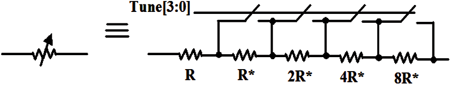
Figure 8: Equivalent circuit of the tunable resistor
4 First Integrator Chopper Negative-R Technique
The input integrator is the most important stage of the CT Δ Σ ADC. The loop filter does not form the first integrator’s non-idealities. The CT Δ Σ ADC’s performance is however directly affected. At the ADC input, several elements produce noise sources. The noisiest components are the amplifier of the first integrator, the RDAC resistors, and the input resistor R1. The ADC input-referred noise can be expressed as [38, 39]
where R1 and RDAC represent ADC ‘s dominant sources of noise to reduce its power consumption. If R1 increases, the linearity of the active-RC filter increases to [40]. R1 is set to 10-kΩ for the ADC and RDAC is set to 4-kΩ. The thermal noise contribution limits the SNR to approximately 102-dB, which is well below the input signal peak value. The first integrator has an integrated capacitance C1 of 8-pF.

Figure 9: Chopper stabilization preamplifier
We suggest using the well-known chopper stabilization method to mitigate the preamplifier’s input-equivalent noise. The chopper stabilization circuit inserted around the preamplifier is shown in Fig. 9 [41, 42]. Two amplifiers compose the preamplifier. The first one depicts the main amplifier,
The auxiliary amplifier enables the main amplifier noise component to be attenuated as
where
The mismatch of the demodulated current spikes and the signal path creates an offset Vos. The capacitance mismatch due to the clock feed generates an AC current spike. The first modulator Mod1 rectifies the resulting AC current. Therefore, it generates a DC spike current at its input. The average current Ioffset value of the measured DC spike can be written as
where Δ C1 and Δ C2 denote the parasitic capacitance of the chopper mismatch, Vclk is the magnitude of the clock signal and fCH is the chopping frequency. This noise is flowing through the series impedance of the input signal source and the chopper stage. Therefore, it is represented by a voltage spike source placed in the amplifier input. The residual offset source Vos can be written as
where R is the input resistance. The residual Vos offset represents the average DC spike value. In addition, a Vos spike voltage signal is generated at the input of modulator Mod1, producing a low-frequency interference. To suppress this interference, we propose to create a proper delay Δ t between the two chopping signals m1(t) and m2(t). Fig. 10 depicts the proposed delay-time chopper stabilization technique [43].

Figure 10: Delay-time chopper stabilization preamplifier
The auxiliary amplifier
where τ = R × Cin. The resistor R is the amplifier input resistance and the capacitor Cin is the amplifier input capacitance.
The main drawback of this approach is the time τ itself. It is much dependent on both the input resistance R and input capacitance Cin of the amplifier. The spike pulse generated by the first modulator Mod1 attack the input of the preamplifier. The preamplifier, then, amplify this resulting spike pulse. Finally, the amplified spike pulse is multiplied with the signal m2(t). Apart from chopping frequency higher-order harmonics, the resulting output signal VY contains a DC component. This DC component depicts the residual offset of the preamplifier caused by the chopping artifacts. A proposed technique to shape this DC spike is added to the chopper stabilization circuit. To solve this problem, a first-order low-pass filter is placed between the auxiliary amplifier

Figure 11: Chopper negative-R stabilization preamplifier
Only 1/f noise is removed by the delayed chopper stabilization. The thermal noise of the auxiliary amplifier
where
where the two parallel resistors R∥ RF depict the negative-R circuit with an important matching coefficient α. If α is closer to 2, the noise opamps decrease ideally by a value of α = 1. The negative-R circuit, in this case, contributes a noise level of
where —H(s)—2 is the noise transfer function of the negative-R with the opamps of Eq. (24). Thus, the chopper negative-R circuit enables mismatch and offset of the opamps to be attenuated.
The Negative-R transistor-level circuit is shown in Fig. 12. It is designed in a bipolar source degeneration topology. It only consumes 12-μW. In this circuit, the degenerated resistor and current source in this topology allow the precision of matching the circuit within 10% to be improved. In addition, a robust transconductance gm of the transistors of the negative-R circuit is preserved over the process variation with temperature and power supply [41].

Figure 12: Negative-R circuit
We have experimentally characterized a fabricated prototype of the proposed IoT circuit. It is based on an M&NEMS microphone and a CT Δ Σ ADC. The CT Δ Σ ADC circuit is designed in a CMOS 65-nm process with a 1.2-V supply voltage and a 0.1-mm2 silicon area. Due to their high linearity, integrated resistors and capacitors are implemented with high-resistivity poly-resistors components and metal-insulator-metal (MIM) components respectively. Fig. 13 depicts the die microphotograph of the proposed IoT circuit.
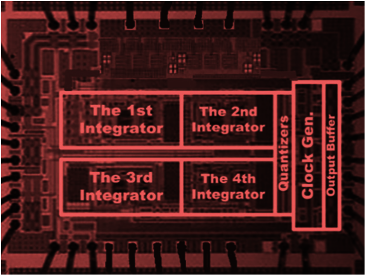
Figure 13: CMOS Δ Σ ADC microphotograph in a 65 nm process and a 0.1 mm2 silicon die area
We propose modifying the first integrator architecture to enhance the SNR, SNDR, and DR of the CT Δ Σ ADC developed in [27]. To reduce both the offset and 1/f noise, a positive feedback two-stage amplifier and a chopper negative-R technique are added to the first integrator. To measure the fabricated M&NEMS resistive microphone, we use the simultaneous comparison technique. To carry out the test of the chip, several measurement devices are used Fig. 14. A calibrated microphone, which acts as a reference microphone, will therefore be included in the test setup. It is located close to the measured M&NEMS microphone to evaluate its output responses. Moreover, we use an anechoic chamber for performing the complete measurement setup to isolate undesirable external phenomena. The M&NEMS microphone and the reference microphone are placed at a distance of one meter in front of the loudspeaker in the anechoic chamber. For measurement, the loudspeaker produces a sound that is used as a reference point at a frequency of 1-kHz. An EQ curve is used to achieve an equivalent response from the loudspeakers at all frequencies. The AP 2700 audio analyzer is coupled to both the M&NEMS microphone output and the B&K Type 2250 Analyzer output. An SRS-CG635 clock generator produces a precise clock with a range of less than 1-ps. We have also introduced an FPGA decimator filter for easier measurement results. The output of the filter attacks the sound analyzer AP 2700 with a serial audio interface.
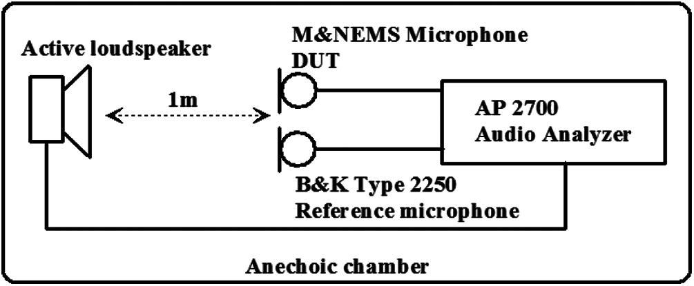
Figure 14: Measurement setup of the M&NEMS microphone system
The loudspeaker’s sound pressure is set at 94-dB. It has a sound frequency of 1-kHz. The instrument B&K analyzer allows detecting the intensity level of the generated sound. The sound level of 94-dB leads to a 1-Pa acoustic sound pressure level. The EQ curve allows correcting the frequency response to achieve a constant level. The frequency level of the neighbor reference microphone is then set at 1-kHz. The measurement result of the M&NEMS microphone in the 20-kHz frequency bandwidth to the reference frequency is presented in Fig. 15. The 94-dB sound pressure level corresponds to the 0-dB normalized response. It is obvious from Fig. 15 that the M&NEMS microphone has an approximately 20-kHz flat analog output response. In the second step, we perform the CT Δ Σ ADC measurements to define the peak SNR, peak SNDR, and it’s DR.
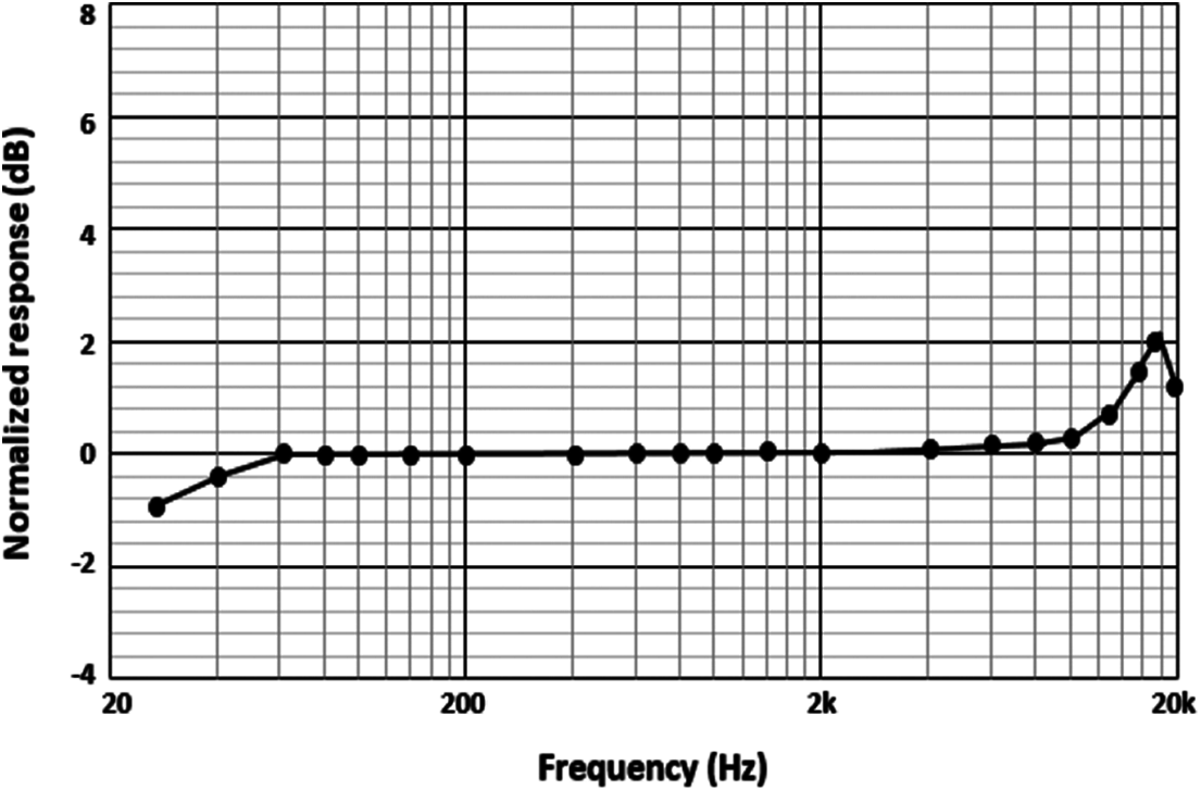
Figure 15: M&NEMS microphone response vs. frequency with a 94-dB sound source level and a 20-kHz bandwidth
We have measured SNR and SNDR of the CT Δ Σ ADC vs. the input signal. The measurement results are shown in Fig. 16. The measured peak SNR is 102.8-dB with an input magnitude of −1.4-dBFS. The measured peak SNDR is 101.3-dB with an input magnitude of −3.4-dBFS. Furthermore, the measured DR of the CT Δ Σ ADC is 108-dB at 25∘C.

Figure 16: Measurement results of SNR and SNDR
On the other hand, the CT Δ Σ ADC is attacked by an input signal of the magnitude of −3.4-dBFS and a frequency of 1-kHz. The measurement result of the CT Δ Σ ADC output spectrum is depicted in Fig. 17. From the measurement result, it is clear that the CT Δ Σ ADC is stable in the 20-kHz bandwidth. Moreover, the CT Δ Σ ADC reaches a good harmonic distortion (HD). The CT Δ Σ ADC has an overall measured power consumption of about 0.96 mW. The analog part consumes nearly 0.8 mW and the digital part consumes nearly 0.16 mW.
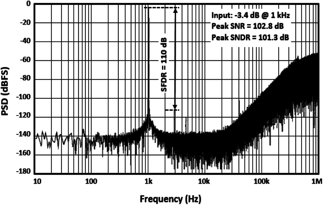
Figure 17: Measurement of the FFT response with a −3.4-dB and 1-kHz input
We also carried out some measurements of the CT Δ Σ ADC performance at various temperatures to determine the influence of the temperature on the fabricated circuit. Measurement results of the SNR and SNDR vs. temperature are presented in Fig. 18. The temperature ranges from 0∘C to 90∘C. From measurement results, the SNR and the SNDR are reduced by only 2-dB if the temperature varies from 0∘C to 90∘C. Therefore, the variation of the temperature does not affect the performance of ADC.
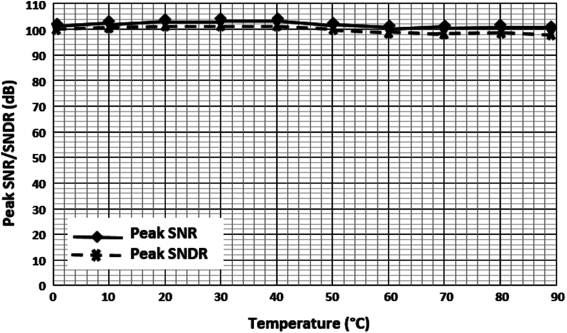
Figure 18: SNR and SNDR of the ADC vs. temperature
Table 1 summarizes the proposed CT Δ Σ ADC measurement results and the comparison with the state-of-the-art. The main advantage of the proposed M&NEMS microphone is that measurement results are done for the complete system composed of the CT Δ Σ ADC and the M&NEMS sensor. However, compared ADCs in the state-of-the-art are measured without the MEMS sensor. Measurement results of the SNR, SNDR, and DR of all other ADCs are near or just over 100-dB [29, 44–48]. On the other hand, our proposed CT Δ Σ ADC reaches a value greater than 100-dB for the same performance. Another important parameter is used to compare the output of the ADC and determine its performance. This parameter is the Schreier figure-of-merit (FOMs), which can be written as [49]

From measurement results, the proposed CT Δ Σ ADC reaches a FOM of 181.2-dB. As a result, the proposed ADC reveals a competitive performance compared to the ADCs of state-of-the-art.
The CMOS interface chip is combined with a fabricated MEMS microphone to verify the performance improvement in the system. The closed-loop test setup uses a shaker table, a data acquisition board, and LABVIEW and MATLAB programs for signal processing. Since the interface electronics uses a high oversampling sigma-delta modulation technique, the PWM output bit stream has to be processed to obtain a useful signal. This is realized by transferring the digital output to a computer by means of a data acquisition board, and processing the signal. The entire system has been operated in closed-loop and the functionality of the system has been verified through extensive tests. The total power consumption is 0.96 mW. Moreover, a noise density of 7 nV/
This paper presents a proposed audio IoT system. A silicon nanowire and a 4th-order single-bit CT Δ Σ ADC are the M&NEMS accelerometer sensor and the CMOS readout interface, respectively. Various low-noise and low-power techniques are proposed to reduce the power consumption and noise of the CT Δ Σ ADC and maintain good performance. A continuous-time loop filter to relax the amplifiers’ settling times replaces the discrete-time loop filter switches of the ADC. The proposed chopper negative-R technique is inserted around the first integrator because it is the noisiest ADC block. This technique allows mitigating the offset and 1/f noise. The first integrator is based on a positive feedback DC-gain enhancement two-stage amplifier, while the second to the fourth integrators is based on a simple fully differential amplifier. The quantizer is embedded in the feedforward coefficients to minimize power consumption and improve performance. The proposed CT Δ Σ ADC is designed in a 65-nm CMOS process with a core area of 0.1-mm2. The supply voltage and the power consumption are respectively 1.2-V and 0.96-mW. The complete audio IoT system is fabricated and measurement results are performed to extract its performances. Over a signal bandwidth of 20-kHz, the CT Δ Σ ADC measurement results reach a peak SNR of 102.8-dB, a peak SNDR of 101.3-dB, and a DR of 108-dB. As a result, the proposed CT Δ Σ ADC becomes one of the best audio ADCs from the result of measurements.
Funding Statement: The authors received no specific funding for this study.
Conflicts of Interest: The authors declare that they have no conflicts of interest to report regarding the present study.
1. Hassija, V., Chamola, V., Saxena, V., Jain, D., Goyal, P. et al. (2019). A survey on IoT security: Application areas, security threats, and solution architectures. IEEE Access, 7, 82721–82743. DOI 10.1109/ACCESS.2019.2924045. [Google Scholar] [CrossRef]
2. Meneghello, F., Calore, M., Zucchetto, D., Polese, M., Zanella, A. (2019). IoT: Internet of threats? A survey of practical security vulnerabilities in real IoT devices. IEEE Internet of Things Journal, 6(5), 8182–8201. DOI 10.1109/JIOT.2019.2935189. [Google Scholar] [CrossRef]
3. Geng, H., Wang, Z., Alsaadi, F. E., Alharbi, K. H., Cheng, Y. (2021). Federated tobit kalman filtering fusion with dead-zone-like censoring and dynamical bias under the round-robin protocol. IEEE Transactions on Signal and Information Processing Over Networks, 7, 1–16. DOI 10.1109/TSIPN.2020.3044904. [Google Scholar] [CrossRef]
4. Geng, H., Wang, Z., Zou, L., Mousavi, A., Cheng, Y. (2021). Protocol-based tobit kalman filter under integral measurements and probabilistic sensor failures. IEEE Transactions on Signal Processing, 69, 546–559. DOI 10.1109/TSP.2020.3048245. [Google Scholar] [CrossRef]
5. Mahalik, N. P. (2008). Mems. New York, USA: Tata McGraw-Hill Education. [Google Scholar]
6. Zhang, Y., Chen, C. H., He, T., Temes, G. C. (2017). A 16 b multi-step incremental analog-to-digital converter with single-opamp multi-slope extended counting. IEEE Journal of Solid-State Circuits, 52(4), 1066–1076. DOI 10.1109/JSSC.2016.2641466. [Google Scholar] [CrossRef]
7. Christen, T. (2013). A 15-bit 140-W scalable-bandwidth inverter-based Δ Σ modulator for a MEMS microphone with digital output. IEEE Journal of Solid-State Circuits, 48(7), 1605–1614. DOI 10.1109/JSSC.2013.2253232. [Google Scholar] [CrossRef]
8. Liu, Y., Hua, S. L., Wang, D. H., Hou, C. H. (2010). A 100 dB-SNR mixed CT/DT audio-band sigma delta ADC. 10th IEEE International Conference on Solid-State and Integrated Circuit Technology (ICSICT), pp. 199–201. Shanghai, China. [Google Scholar]
9. Karmakar, S., Gönen, B., Sebastiano, F., van Veldhoven, R., Makinwa, K. A. A. (2018). A 280 μW dynamic zoom ADC with 120 dB DR and 118 dB SNDR in 1 kHz BW. IEEE Journal of Solid-State Circuits, 53(12), 3497–3507. DOI 10.1109/JSSC.2018.2865466. [Google Scholar] [CrossRef]
10. Zhao, B., Lian, Y., Niknejad, A. M., Heng, C. H. (2019). A low-power compact IEEE 802.15.6 compatible human body communication transceiver with digital sigma-delta IIR mask shaping. IEEE Journal of Solid-State Circuits, 54(2), 346–357. DOI 10.1109/JSSC.2018.2873586. [Google Scholar] [CrossRef]
11. Nandi, T., Boominathan, K., Pavan, S. (2013). Continuous-time Δ Σ modulators with improved linearity and reduced clock jitter sensitivity using the switched-capacitor return-to-zero DAC. IEEE Journal of Solid-State Circuits, 48(8), 1365–1379. DOI 10.1109/JSSC.2013.2259012. [Google Scholar] [CrossRef]
12. Zhang, H., Tan, Z., Chu, C., Chen, B., Li, H. et al. (2019). A 1-V 560-nW SAR ADC with 90-dB SNDR for IoT sensing applications. IEEE Transactions on Circuits and Systems II: Express Briefs, 66(12), 1967–1971. DOI 10.1109/TCSII.2019.2898365. [Google Scholar] [CrossRef]
13. Sansen, W., Steyaert, M., Peluso, V., Peeters, E. (1998). Toward sub-1V analog integrated circuits in submicron standard CMOS technologies. Proceeding International Solid-State Circuits Conference, pp. 186–187. San Francisco, CA, USA. [Google Scholar]
14. Montree, K., Thanat, N., Fabian, K. (2018). Low-power sample and hold circuits using current conveyor analogue switches. IET Circuits, Devices & Systems, 12(4), 397–402. DOI 10.1049/iet-cds.2017.0411. [Google Scholar] [CrossRef]
15. Nebhen, J., Ferreira, P. M., Mansouri, S. (2020). A chopper stabilization audio instrumentation amplifier for IoT applications. Journal of Low Power Electronics and Applications, 10(2), 13. DOI 10.3390/jlpea10020013. [Google Scholar] [CrossRef]
16. Robert, P., Walther, A. (2014). MEMS dynamic pressure sensor, in particular for applications to microphone production. U.S. Patent 8783113B2. https://patents.google.com/patent/US8783113. [Google Scholar]
17. Jian, H. Y., Xu, Z., Wu, Y. C., Chang, M. C. (2010). A fractional-N PLL for multiband (0.8–6 GHz) communications using binary-weighted D/A differentiator and offset-frequency Δ -Σ modulator. IEEE Journal of Solid-State Circuits, 45(4), 768–780. DOI 10.1109/JSSC.2010.2040232. [Google Scholar] [CrossRef]
18. Barlian, A. A., Park, W. T., Mallon, J. R., Rastegar, A. J., Pruitt, B. L. (2009). Review: Semiconductor piezoresistance for microsystems. Proceedings of the IEEE, 97(3), 513–552. DOI 10.1109/JPROC.2009.2013612. [Google Scholar] [CrossRef]
19. Blazquez, G., Pons, P., Boukabache, A. (1989). Capabilities and limits of silicon pressure sensors. Sensors and Actuators, 17(34), 387–403. DOI 10.1016/0250-6874(89)80026-5. [Google Scholar] [CrossRef]
20. Liu, C. (2006). Foundations of MEMS. Hoboken, USA: Pearson Prentice Hall. [Google Scholar]
21. Mohammed, A. A. S., Moussa, W. A., Lou, E. (2010). Optimization of geometric characteristics to improve sensing performance of mems piezoresistive strain sensors. Journal of Micromechanics and Microengineering, 20(1), 15. DOI 10.1088/0960-1317/20/1/015015. [Google Scholar] [CrossRef]
22. Sun, Y. C., Gao, Z., Tian, L. Q., Zhang, Y. (2004). Modelling of the reverse current and its effects on the thermal drift of the offset voltage for piezoresistive pressure sensors. Sensors and Actuators A: Physical, 116(1), 125–132. DOI 10.1016/j.sna.2004.01.064. [Google Scholar] [CrossRef]
23. He, R., Yang, P. (2006). Giant piezoresistance effect in silicon nanowires. Nature Nanotechnology, 1(1), 42–46. DOI 10.1038/nnano.2006.53. [Google Scholar] [CrossRef]
24. Zhou, D., Briseno-Vidrios, C., Jian, J., Park, C., Liu, Q. et al. (2019). A 13-bit 260 MS/s power-efficient pipeline ADC using a current-reuse technique and interstage gain and nonlinearity errors calibration. IEEE Transactions on Circuits and Systems I: Regular Papers, 66(9), 3373–3383. DOI 10.1109/TCSI.2019.2925743. [Google Scholar] [CrossRef]
25. Maloberti, F. (2007). Data converters. Dordrecht, The Netherlands: Springer Science & Business Media. [Google Scholar]
26. Malcovati, P., Baschirotto, A. (2018). The evolution of integrated interfaces for MEMS microphones. Micromachines (Basel), 9(7), 323. DOI 10.3390/mi9070323. [Google Scholar] [CrossRef]
27. Zhang, J., Lian, Y., Yao, L., Shi, B. (2011). A 0.6-V 82-dB 28.6-μW continuous-time audio delta-sigma modulator. IEEE Journal of Solid-State Circuits, 46(10), 2326–2335. DOI 10.1109/JSSC.2011.2161212. [Google Scholar] [CrossRef]
28. Yao, L., Steyaert, M., Sansen, W. (2005). A 1-V, 1-MS/s, 88-dB sigma-delta modulator in 0.13-μm digital CMOS technology. IEEE Xplore. VLSI Technology and Circuits Digest of Technical Papers, pp. 180–183. Kyoto, Japan. [Google Scholar]
29. Leow, Y. H., Tang, H., Sun, Z. C., Siek, L. (2016). A 1 V 103 dB 3rd-order audio continuous-time delta sigma ADC with enhanced noise shaping in 65 nm CMOS. IEEE Journal of Solid-State Circuits, 51(11), 2625–2638. DOI 10.1109/JSSC.2016.2593777. [Google Scholar] [CrossRef]
30. Nebhen, J., Masmoudi, M., Rahajandraibe, W., Aguir, K. (2019). High DC-gain two-stage OTA using positive feedback and split-length transistor techniques. In: Alfaries, A., Mengash, H., Yasar, A., Shakshuki, E. (Eds.Advances in data science, cyber security and IT applications, pp. 286–302. Cham: Springer. [Google Scholar]
31. Yavari, M. (2005). Hybrid cascode compensation for two-stage CMOS opamps. IEICE Transactions on Electronics, 88, 1161–1165. DOI 10.1093/ietele/e88-c.6.1161. [Google Scholar] [CrossRef]
32. Ferreira, L. H. C., Pimenta, T. C., Moreno, R. L. (2007). An ultra-low-voltage ultralow-power CMOS miller OTA with rail-to-rail input/output swing. IEEE Transactions on Circuits and Systems II: Express Briefs, 54(10), 843–847. DOI 10.1109/TCSII.2007.902216. [Google Scholar] [CrossRef]
33. Assaad, R. S., Silva-Martinez, J. (2007). Enhancing general performance of folded-cascode amplifier by recycling current. Electronics Letters, 43(23), 1–2. DOI 10.1049/el:20072031. [Google Scholar] [CrossRef]
34. Nebhen, E. S. J., Rahajandraibe, W., Dufaza, C., Meillere, S., Kussener, E. et al. (2013). Low-noise smart sensor based on silicon nanowire for MEMS resistive microphone, pp. 1–4. Baltimore, MD: IEEE SENSORS. [Google Scholar]
35. Johns, D., Martin, K. (1997). Analog integrated circuit design. New York, USA: John-Wiley & Sons. [Google Scholar]
36. Qing, X., Li, W., Wang, Y., Sun, H. (2019). Piezoelectric transducer-based structural health monitoring for aircraft applications. Sensors, 19(3), 545. DOI 10.3390/s19030545. [Google Scholar] [CrossRef]
37. AlMarashli, A., Anders, J., Becker, J., Ortmanns, M. (2018). A nyquist rate SAR ADC employing incremental sigma delta DAC achieving peak SFDR = 107 dB at 80 kS/s. IEEE Journal of Solid-State Circuits, 53(5), 1493–1507. DOI 10.1109/JSSC.2017.2776299. [Google Scholar] [CrossRef]
38. Gönen, B., Karmakar, S., van Veldhoven, R., Makinwa, K. A. A. (2020). A continuous-time zoom ADC for low-power audio applications. IEEE Journal of Solid-State Circuits, 55(4), 1023–1031. DOI 10.1109/JSSC.2019.2959480. [Google Scholar] [CrossRef]
39. Burt, R., Zhang, J. A. (2006). Micropower chopper-stabilized operational amplifier using a SC notch filter with synchronous integration inside the continuous-time signal path. IEEE Journal of Solid-State Circuits, 41(12), 2729–2736. DOI 10.1109/JSSC.2006.884195. [Google Scholar] [CrossRef]
40. Samadpoor Rikan, B., Kim, S. Y., Ahmad, N., Abbasizadeh, H., Riaz Ur Rehman, M. et al. (2018). A sigma-delta ADC for signal conditioning IC of automotive piezo-resistive pressure sensors with over 80 dB SNR. Sensors, 18(12), 4199. DOI 10.3390/s18124199. [Google Scholar] [CrossRef]
41. Lee, H. S., Nguyen, V. N., Pham, X. L., Lee, J. W., Park, H. K. (2017). A 250-μW, 18-nV/
42. Chandrakumar, H., Markovic, D. (2017). A high dynamic-range neural recording chopper amplifier for simultaneous neural recording and stimulation. IEEE Journal of Solid-State Circuits, 52(3), 645–656. DOI 10.1109/JSSC.2016.2645611. [Google Scholar] [CrossRef]
43. Nebhen, J., Alnowaiser, K., Meillere, S. (2020). A 5-nV/
44. Sukumaran, A., Pavan, S. (2014). Low power design techniques for single-bit audio continuous-time delta sigma ADCs using FIR feedback. IEEE Journal of Solid-State Circuits, 49(11), 2515–2525. DOI 10.1109/JSSC.2014.2332885. [Google Scholar] [CrossRef]
45. Wang, T. C., Lin, Y. H., Liu, C. C. (2015). A 0.022 mm 98.5 dB SNDR hybrid audio Δ Σ modulator with digital ELD compensation in 28 nm CMOS. IEEE Journal of Solid-State Circuits, 50(11), 2655–2664. DOI 10.1109/JSSC.2015.2453953. [Google Scholar] [CrossRef]
46. Gönen, B., Sebastiano, F., Quan, R., van Veldhoven, R., Makinwa, K. A. A. (2017). A dynamic zoom ADC with 109-dB DR for audio applications. IEEE Journal of Solid-State Circuits, 52(6), 1542–1550. DOI 10.1109/JSSC.2017.2669022. [Google Scholar] [CrossRef]
47. Billa, S., Sukumaran, A., Pavan, S. (2017). Analysis and design of continuous-time delta-sigma converters incorporating chopping. IEEE Journal of Solid-State Circuits, 52(9), 2350–2361. DOI 10.1109/JSSC.2017.2717937. [Google Scholar] [CrossRef]
48. Chandrakumar, H., Markovic, D. (2018). A 15.2-ENOB 5-kHz BW 4.5-μW chopped CT Δ Σ-ADC for artifact-tolerant neural recording front ends. IEEE Journal of Solid-State Circuits, 53(12), 3470–3483. DOI 10.1109/JSSC.2018.2876468. [Google Scholar] [CrossRef]
49. Schreier, R., Temes, G. C. (2005). Understanding Δ Σ data converters. New-York, NY, USA: Wiley-Interscience. [Google Scholar]
 | This work is licensed under a Creative Commons Attribution 4.0 International License, which permits unrestricted use, distribution, and reproduction in any medium, provided the original work is properly cited. |