DOI:10.32604/cmc.2021.016133
| Computers, Materials & Continua DOI:10.32604/cmc.2021.016133 | |
| Article |
A Compact Dual-Port Multi-Band Rectifier Circuit for RF Energy Harvesting
1Centre for Wireless Technology, Faculty of Engineering, Multimedia University, Cyberjaya, 63100, Malaysia
2Department of Medical Equipment Technology, College of Applied Medical Sciences, Majmaah University, AlMajmaah, 11952, Saudi Arabia
3Department of Physics, Microwave Electronics Research Laboratory, Faculty of Mathematical, Physical and Natural Sciences of Tunis, Tunis El Manar University, Tunis, 2092, Tunisia
*Corresponding Author: Surajo Muhammad. Email: doguwa_2002@yahoo.com
Received: 24 December 2020; Accepted: 24 January 2021
Abstract: This paper presents a compact multi-band rectifier with an improved impedance matching bandwidth. It uses a combination of
Keywords: RF energy harvesting; impedance matching network; power conversion efficiency; multi-band rectifier; dual-port; power management module
The technological advancement and widespread in wireless communication have increased the need for low-powered internet of things (IoT) devices, and sensor nodes [1,2]. These devices are usually operated by batteries, and it is undesirable to provide a significant number of nodes with batteries because of their maintenance cost for charging or replacement. The abundance of electromagnetic (EM) power sources radiated into space from various wireless equipment appears to be a promising source of energy through RFEH technique [1–3]. RFEH has become an emerging technology for handling low powered electronic devices through the process of battery-less (direct power) and wireless charging for driving other wireless node [2,4]. The RFEH module comprises a rectifying antenna (rectenna), with two segments, namely an antenna and a rectifying circuit. The rectifying circuit is the significant part of the RFEH node comprising an IMN, a rectifying diode, a dc-pass filter, and a terminal load [2]. RFEH system offers several advantages over other forms of energy harvesting (EH) method. In fact, it has lightweight, flexibility for movement, continuous supply, and independent of light. Moreover, it is integrable and scalable with other nodes with less environmental influence [1,4].
Over the years, various research works on rectenna and rectifier circuits have been proposed for single-band [2,3], dual-band [5], and multi-band operations [6,7]. The widely deployed frequency bands for the RFEH system include GSM/900, GSM/1800, UMTS/2100, Wi-Fi/2.45, and LTE/2600 because of their significant contributions for the RF available power extracted by the RFEH node. The independent and autonomous attributes associated with the IoT devices, and sensor nodes, makes the deployment of a single frequency source RF harvester ineffective [6,8]. Because of the random and unpredictable nature of the received RF signal, and any form of signal distortion on the specified frequency creates energy losses that can lead to a node or device failure [8]. Using multi-band RF rectifier circuits provide a significant improvement over the single-band and dual-band operation because of the energy contributions from each frequency tone [9]. Most of the reported designs in [10,11] are associated with narrow operational bandwidth. Hence, the RF harvester performance is greatly affected when the operating frequency shifts because of components loss, parasitic capacitance, and signal propagation. Using an efficient rectifier with wideband characteristics is considered being a promising approach for a reliable RFEH system [11,12]. The RF spectral survey from the open literature in [10–13] shows that designing a broadband rectifier with the ability to collects much of the available RF energy across the EM spectrum is a potential candidates to achieve a sustainable power source [14].
Minimal available RF power density, impedance mismatch, non-linear resistance of a diode, a variation of the circuit performance with the operating frequency, and a terminal load are some of the major challenges in rectifier design [1]. These challenges have been addressed over the past few years from several literature studies [1–15]. The authors in [1] reported an RFEH circuit with the manually adjustable MN using trimmers with 4-stage voltage multiplier operating at 0.7, 0.85, and 0.9 GHz. The design achieved a peak PCE of 41%, 40%, and 42% for 0 dBm at the three variable frequencies, respectively. The design approach is impractical because of the maintenance cost to manually match the antenna with rectifying circuits in the current trends of RFEH module applications involving large sensor networks and IoT devices. In [9], the authors presented a triple-band (1.84, 2.14, and 2.45 GHz) RF harvester with a maximum efficiency achieved at 25.3%, 27.9%, and 19.3% for −20 dBm, respectively, using a complex 16 ports antenna connected to 8 individual rectifiers. In [10], the authors proposed a triple-band rectifier operating at 0.85, 1.77, and 2.07 GHz using an impedance matching transformer, and the rectifier achieved a maximum PCE of 61.9%, 71.5%, and 60.5% for 0 dBm input power, respectively. The authors in [16] presented a triple-band RF harvester operating at 2 2.5, and 3.5 GHz, and the design achieved a maximum PCE of 53%, 31%, and 15.56% at −7 dBm input power, respectively. The designed frequency at 2 GHz and 3.5 GHz is associated with minimal power density for extraction by the RFEH node. A multiband RFEH module is considered to be a suitable candidate for achieving a robust RFEH module, with a reliable power source, because of the available power density contributed by each frequency tone [9]. The authors in [17] reported a four-band (0.89, 1.27, 2.02, and 2.38 GHz) rectifier using a series diode D1, and a shunt combination of field-effect transistor (FET) with another diode D2. The design recorded an RF-to-DC PCE of 47.8%, 33.5%, 49.7%, and 36.2%, at each respective frequency for −10 dBm input power. The authors in [18] present a quad-band (0.95, 1.83, 2.45, and 2.62 GHz) rectifier, using a pair branch of 4-stage voltage multiplier. The rectifier attained maximum RF-to-DC PCE of 44.8%, 27.5%, 28%, and 24.2% for 10 dBm input power, respectively. The additional parasitic capacitance from FET in [17], and multiple components in [18] degrade the rectifier performance. The designed frequency by the authors in [16] at 2 and 3.5 GHz, and [17] at 1.27 GHz is associated with minimal power density for extraction by the RFEH node. The authors in [19] also proposed a quad-band (1.3, 1.7, 2.4, and 3.6 GHz) rectifier through a T-section distributed MN, and the work realized a peak PCE of 54% at 1.7 GHz for 10 dBm. The proposed design is suitable for the high power RFEH module, and the reduced circuit performance is largely attributed to parasitic capacitance across the rectifier junction besides harnessing minimal available RF power density at (1.3 and 3.6 GHz). To improved RF-to-DC PCE, the authors in [9,20] exploits the potential of a spatial domain through multi-port/multiple antennas, and a dc combining from multiple rectifiers outputs for transforming the intercepted EM signal into usable dc outputs. The authors in [20] proposed a quad-band (98 MHz, 0.88, 1.7 and 2.370 GHz) rectenna using two independent circuits to harvest RF signal through dc combining. The low-frequency rectifier harvest frequency modulated (FM) signals efficiently at the line of sight (LOS) with a narrow operational bandwidth of 10 MHz, and achieved a peak RF-to-DC PCE of 80% for −6 dBm with a total size of (35 mm
This paper proposes a compact dual-port rectifier that covers (GSM/900, GSM/1800, UMTS/2100, Wi-Fi/2.45, and LTE/2600) in the EM spectrum, matched with a 2 k
• The work presents, to the best of our knowledge, a compact and efficient multi-band rectifier as compared to the state-of-the-art rectifiers.
• The synchronous harvesting of RF signal for optimal and sustainable RFEH module by exploiting spatial and frequency domain.
• We present a unique IMN in the upper frequencies using a combination of a meandered line (MDL), a shunt radial stubs, a shunt-curve impedance transformer with a series inductor to enhance the rectifier efficiency with a minimum junction capacitance across the rectifier branch.
• Enhanced rectifier bandwidth to cover most of the significant spectrum in the RFEH system design for optimal and reliable extraction of ambient RF input signal from the multiple signal tones. This is guided by the RF spectral survey carried out in this work and the open literature.
This paper is organized as follows. Section 2 presents design architecture of the multi-band rectifiers. Section 3 outlines the structure, specifications, and the circuit layout of the RFEH rectifier. Section 4 provides results discussion, indoor and outdoor performance analysis of the proposed rectifier. Section 5 concludes the paper.
The prime objective of the RFEH system is to transform the received RF signals from the ambient sources into a usable dc power source with minimal losses [1,4,10]. The performance of the RF harvester (single-band or multiband) is considerably reduced when the operating frequency shifted from the optimal design level. Multiple RFEH circuits have been studied and proposed in the literature [1–3,8,14–20]. The use of uniform antenna arrays and a multi-port antenna are deployed in rectenna circuits to handle spatial domain for enhancing the received RF signals from the ambient environment. The overall dc output signal is realized through RF combination of the antenna outputs or combining the dc outputs from multiple rectifiers [9]. Fig. 1a presents an RFEH architecture that collects the received RF power from a set of uniform gain antennas or a single antenna array, which is then delivered to the rectifier through BALUN. The approach needs a rectifying diode with a large breakdown voltage to accommodate more power at the expense of a large parasitic capacitance across the rectifier junction, which degrades the overall RF-to-dc PCE [20]. Uniform antenna arrays are normally associated with large elements spacing to address mutual coupling, resulting in a large antenna electrical size [9]. For example, the work in [5] proposed a dual-band (1.8 and 2.5 GHz) rectenna using an antenna array of size 264 mm
The proposed design architecture in Fig. 1c is applied in this work because of the rectifier ability to exploit both spatial and frequency domains using RF and dc combinations. The architecture exploits the spatial domain through dual-port configuration with the ability to receive RF signal from the ambient environment, and the frequency domain is exploited through multiple operating frequencies with a good operational bandwidth to cover a wide frequency spectrum for a reliable RFEH node. The idea is to deploy a narrow band rectifier tuned around 900 MHz using lumped MN in the first segment (Rectifier-1). The second section of the rectifier (Rectifier-2) covers a wider operating frequency between (1.7 to 2.7 GHz) through a combination of distributed and lumped MN. The overall energy transformed by the power harvesting circuits is integrated by the dc combiner, which can be utilized by a practical load such as a low-powered dc/dc converter and sensor node. The design approach ensures less circuit complexity from each rectifier block for efficient RF harvester.

Figure 1: RFEH design architecture: (a) With RF-combined antennas, and a single multi-band rectifier, (b) with individual rectifying antennas integrated through a dc combiner, (c) proposed hybrid topology
The deployment of high frequency (HF) rectifying diode for low-power applications in the RFEH system requires reliability and the capability of the circuit to manage energy conversion with a minimum dissipation [22]. The RF-to-DC PCE of a rectifying antenna primarily depends on a rectifying circuit [21]. Rectifier topology can be configured in different types of the circuit layout. Single series diode and voltage multiplier are the two widely used topologies. A voltage multiplier can be modeled and cascaded as Dickson/Greinacher or Villard/Cockcroft–Walton rectifier, and are mostly considered for a high powered RFEH circuits [4,20]. Single series diode configuration demonstrates higher RF-to-DC PCE at low input power levels because of low junction capacitance and a faster switching time [4–10]. Hence, the proposed rectifier is designed based on a single series diode alongside a shunt DC-pass capacitor filter with the terminal load, as depicted in Fig. 2.

Figure 2: Conventional single series rectifier topology for RFEH circuit
Fig. 3 presents a schematic of the proposed multi-band rectifier using a dual-port configuration. The matching from each port is designed using a unique IMN approach to reduce circuit complexity and achieved compactness. The first segment of the rectifier (Rectifier-1) is achieved using a simple

Figure 3: Proposed EM model layout of the rectifier
The proposed rectifier segments are designed using a single series HSMS-2850 Schottky barrier diode from Avago having a SOT-23 physical layout. The diode is a fast switching device suitable for low-powered RF applications, with the ability to operate at high frequency, with a minimum junction capacitance, and a low forward-biased voltage of 0.18 pF, and 150 mV, respectively [2,10]. Eq. (1) Describes a relationship for the junction capacitance driven by an operating frequency fc, and input voltage Vin over a period of time t. A DC-pass filter and a terminal load are the remaining parts of the rectifier, which are designed and constructed on a 1.575 mm thick RT/Duroid 5880 substrate, (with a dielectric constant of 2.2, and a minimum loss tangent of 0.0009). The rectifier is connected to a 50
where C is the capacitance of the capacitor with current I passing through junction diode at the rate of nonlinear voltage “V”.
Each segment of the rectifier undergoes a preliminary design in advance design system (ADS) without a MN, having only a rectifying diode, dc-pass capacitor filter, and a terminal load. The dc-pass filter is designed to prevent the entrance of higher-order harmonics into the terminal load [21]. The load terminal RL is primarily a frequency-dependent and complex in nature [9]. A source pool simulation is conducted to evaluate the appropriate value of the load terminal in ADS using a harmonic balance solver, and a 2 k
Fig. 4a presents a simplified simulation setup to compute the values of the diode input impedance (Zin = Rin + jXin) from each cell block. For this study, a power level of −10 dBm is considered because the average input power between the conventional transceiver is within −10 dBm reference point, taking RF link loss into account [11–13,17]. The values of Zin at the four (0.94, 1.8, 2.1, 2.45 GHz) operating frequencies are (169.90 – j644.6, 59.84 – j340.21, 46.30 – j288.15, 37.82 – j242.12). The rectifier input impedances are then matched to 50

Figure 4: (a) Input impedance simulation setup for operating frequency fc (b) impedance matching and the rectifier input impedance equivalent circuits
The input signal from Port-1 at 50
By splitting the impedance X2 for the inductor L2 into two portions (X2a, and X2b) such that
Looking into Portion-1, the quality factor Q1 is given by:
where conductance Gin = 1/Rin.
The elements of the matching section X2b and B1 are determined by canceling the imaginary part of the impedance and equating the real part at the operating frequency.
L2b, and C1 are calculated as:
where Bin =
Looking into Portion-2 of the matching section, the quality factor Q2 is given by:
The elements of the matching section B2 and X2b are determined by:
L1, and L2a are also calculated as:
L2 is computed by adding Eqs. (5) and (11) as:
The overall quality factor Q of the network is the summation of the two quality factors Q1, and Q2 (Q = Q1+Q2).
The parameters of the
The input impedance of the diode is frequency-dependent with a narrow bandwidth for a conventional MN [6]. The proximity of the GSM/1800, UMTS/2100, and Wi-Fi/2.45 frequency bands in the EM spectrum make a rectifier design with a reliable input impedance bandwidth across those bands a quite challenging task [9]. The approach of integrating two or more single band rectifiers in parallel to cover a wide range of frequencies with good impedance bandwidth is reported in [7–15,21]. This is a key to ensure maximum power transfer to the terminal load with a reliable contribution from each signal tone. Consequently, the second rectifier segment (Rectifier-2) is designed based on the aforementioned approach, comprising three cell blocks (Cell-1, Cell-2, and Cell-3) connected in parallel through Port-2.
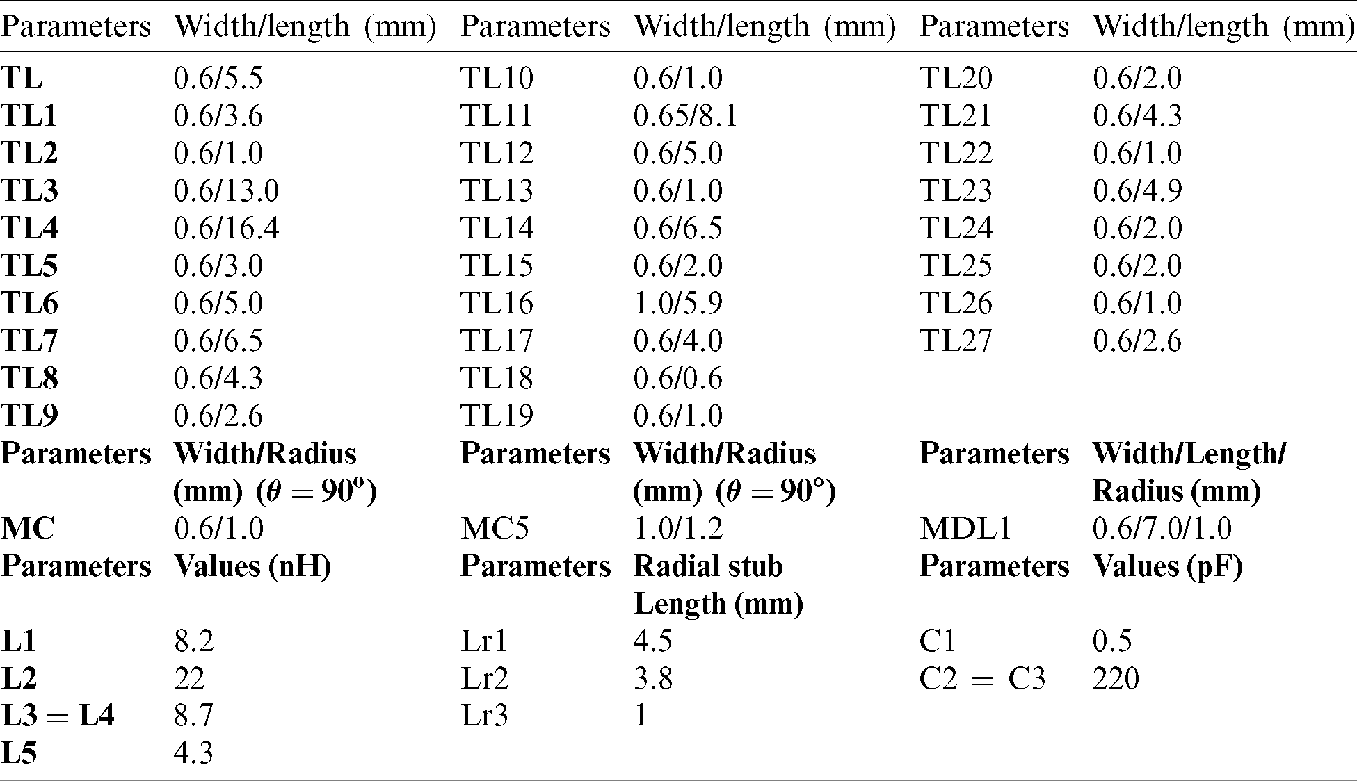
Table 1: Dimensions and parameters of the proposed rectifier
A single band MN operating at 1.8, 2.1, and 2.45 GHz is initially designed to match a single series diode to 50
The corresponding output dc signals from the two ports are connected to the load terminal RL by a simple dc combiner. The overall rectifier circuit is achieved from a combination of five (5) inductors, three (3) capacitors, four (4) diodes, and a load terminal RL.
The whole designed rectifier undergoes fine-tuning and optimization to minimize the effects of additional parasitics (such as SMA source connector, interconnecting transmission lines, soldering, and chip component tolerance losses) that are not considered in the simulation. Tab. 1 presents the optimized parameters of the proposed multi-band rectifier.
Fig. 5a presents the fabricated rectifier prototype using full ground architecture. A pair of crocodile clip connects the rectifier across the terminal load to evaluate the output performance. The rectifier occupies a space of 29.9 mm

Figure 5: (a) Fabricated prototype of the proposed rectifier. (b) Simulated and measured reflection coefficient S11 against frequency for the proposed multi-band rectifier at Port-1, and Port-2
Fig. 6 presents the measured and simulated RF-to-dc PCE of the proposed rectifier. The measured result is realized through frequency sweeping between 0.8 to 2.8 GHz for 0 dBm, −10, −20, and −30 dBm input power levels across the 2 k

Figure 6: Simulated and measured RF-to-dc PCE sweep against frequency at different RF input power levels Pin summed from Port-1and Port-2
The RF-to-dc PCE of the rectifier at each port is computed from the measured output dc voltage as:
where
The overall RF-to-DC PCE of the rectifier from the two ports is obtained from:
where
Figs. 7a and 7b shows the simulated and measured RF-to-dc PCE of the proposed multi-band rectifier against the available RF power source. The rectifier achieved measured peak RF-to-DC PCE of 82.3% for 3 dBm at 0.92 GHz, and 72.4%, 74.5%, 73.9%, and 67.7% for 4, 0, 1 and −1 dBm at 1.82 GHz, 2.1 GHz, 2.46 GHz, and 2.65 GHz, respectively. To demonstrate the rectifier capability under low power condition, it can also be shown that the fabricated prototype realizes a maximum RF-to-DC PCE of 31.8%, 24%, 22.7%, 15%, and 14.1% for −20 dBm at the five operating frequencies, respectively. The RF-to-DC PCE at the upper frequency slightly drops mainly because of the losses associated with diodes and PCB at higher operating frequencies [15].

Figure 7: Simulated and measured RF-to-dc PCE against input power Pin at: (a) 0.92, 1.82 and 2.1 GHz (b) 2.46 and 2.65 GHz
Fig. 8 provides the measurement setups of the proposed rectifier. The measurement of the S11 and the output dc voltage were taken separately for each rectifier at Port-1 and Port-2, as previously discussed in this section.

Figure 8: Multi-band rectifier fabricated prototype and measurement setups for Port-1 and Port-2
Fig. 9 shows the RF-to-DC PCE performance of the multiband rectifier sweep against load terminal RL for 0 dBm input source. The proposed rectifier attained a maximum RF-to-dc PCE between the range of 1.2 k

Figure 9: Multi-band rectifier RF-to-DC PCE against terminal load RL for 0 dBm
The measurement of the rectifier performance in ambiance environment is conducted in Multimedia University, Cyberjaya Campus. The distance and height between the testing site and the nearby cell tower (BS) are approximately 175 and 2 m, respectively. The first ambient test setup is carried out using two pairs of commercial whip antenna from ABRACON with a serial number (AEACAD097015-S698), and the antenna operates between (700 to 2700 MHz) with a 5 dBi gain. The efficiency of the antenna within the operating frequencies range is between 65%–58%, respectively. Fig. 10a presents the measurement setup for Rectifier-1 at Port-1, and Rectifier-2 at Port-2, using a single whip antenna, and a pair of the whip antenna is also connected at Port-1 and Port-2, respectively. The RF power densities is also measured during the ambient evaluation, through a 6 GHz RF spectrum analyzer from Aim (TTi PSA6005). The received power recorded around GSM/900, GSM/1800, UMTS/2100, Wi-Fi/2.45, and LTE/2600 by the spectrum analyzer varies between (−37 to −18 dBm, −35 to −15 dBm, −45 to −20 dBm, −50 to −20 dBm, and −45 to −20 dBm), respectively. From the reported RF power densities, the multi-band rectifier records an output dc voltage of 86.5, 398, and 454 mV for a single port connection at Port-1 and Port-2, and from a combination of the two ports, respectively.

Figure 10: Proposed rectifier ambiance measurement setups: (a) Ambiance only with bq25504-674 (b) Ambiance with bq25504-674
The second phase of the measurement is carried by introducing a PMM into the output of the rectifier. The ambient RF input signal generated by the antenna can be characterized as a multi-tone signal source, with variable levels of power that fluctuate over the range of design frequency. Additionally, the output impedance of the rectifier is a time-varying signal that requires a system with effective power buffering such as supercapacitor and micro-batteries through PMM to maintain a stable circuit operation [4,23]. A low power PMM bq25504-674 evaluation module (EVM) from Texas Instruments is deployed in this work. The module runs a programmable maximum power point tracking (MPPT) sampling network for optimal power transfer into the circuit. The module can detect a low startup input voltage of 130 mV for a cold-start, and 330 mV for a hot-start at a minimal quiescent current of 330 nA. The minimum cold-start input power required for the module to start a normal charging is −30 dBm. The bq25504 module is integrated with a boost dc–dc converter that can generate up to 3.1 V practical voltage levels. The EVM is also incorporated with a built-in battery management module that is deployed to manage the output power duty cycle to the load [23].
Fig. 10b shows the rectifier ambient measurements setup with the bq25504-674 EVM, and the proposed design setup achieved an output dc voltage of 351 mV for Port-1, 0.851 V for Port-2, and 1.214 V from the two-port connections.
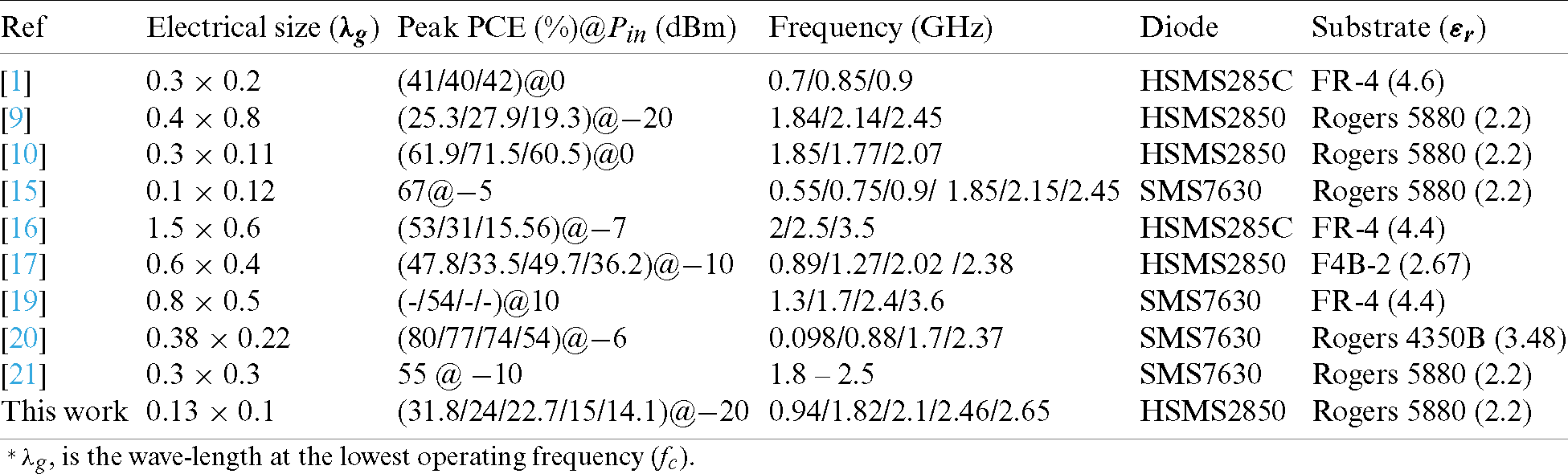
Tab. 2 provides a comparison of the proposed multiband dual-port rectifier with other related works reported in the literature. The manual configuration of the MN reported by the authors in [1] is impractical. As seen in [10], the rectifier operational bandwidth is relatively narrow. The RF-to-dc PCE reported in [1,10] for an input power of 0 dBm across the designed operating frequencies is lower than that of the proposed design besides large electrical length. Our proposed work achieved 80.5%, 64%, 74.5%, 73.9%, and 62.4% measured RF-to-dc PCE for 0 dBm at the five operating frequencies, respectively. Although the authors in [9] reported an improved RF-to-DC PCE for −20 dBm at three operating frequencies. Our proposed work offers a better operational bandwidth across five operating frequencies. The designed frequency by the authors in [17] at 1.27 GHz and [19] at 3.6 GHz has a low power density for extraction. Additionally, the proposed designs achieved peak RF-to-DC PCE at 10 dBm, which is suitable for high-power RFEH system. It can be pointed out that our proposed design exhibits better compactness and an improved RF-to-DC PCE as compares to the work reported by the authors in [16,17,19]. A single-band rectifier reported by the authors in [20] at 98 MHz requires a direct LOS to operate. The wideband rectifier reported by the authors in [21] can only harvest RF signals at GSM/1800, UMTS/2100, and Wi-Fi/2.45 frequency bands. The proposed rectifier in this paper covers two additional operating frequencies at (0.92 and 2.65 GHz) with less electrical length and an improved RF-to-dc PCE as compares to the work reported in [9,21]. Using single dual-diode and sixth-order lumped elements MN across the three cell branches reported by the authors in [15] lowers the overall RF-to-DC PCE of the circuits. The frequency domain in [15,20] is not well exploited because of the narrow bandwidth across the operating frequencies besides the large electrical length from the two separate rectifiers in [20].
Table 2: Comparison of the proposed rectifier with the related work
The proposed multi-band rectifier demonstrates an improved RF-to-dc PCE. The fabricated rectifier prototype achieves over 64% PCE across the operating frequencies for an input power of 0 dBm. The design shows a better −10 dB operational bandwidth with the ability to extract practical RF signal across the designed frequencies than most of the reported work in the literature. The design also shows compactness and the capability of the circuit to drive a low-powered PMM using bq25504-674 EVM.
A multi-band rectifier with dual-port configuration is reported in this work. To match the input impedance of the rectifier to a 50
Funding Statement: This work was supported by TM R&D Malaysia under project number MMUE/190001.
Conflicts of Interest: The authors declare that they have no conflicts of interest to report regarding the present study.
1. U. Muncuk, K. Alemdar, J. D. Sarode and K. R. Chowdhury. (2018). “Multiband ambient RF energy harvesting circuit design for enabling batteryless sensors and IoT,” IEEE Internet of Things Journal, vol. 5, no. 4, pp. 2700–2714. [Google Scholar]
2. S. Muhammad, J. J. Tiang, W. S. Kin, A. Iqbal, M. Alibakhshikenari et al. (2020). , “Compact rectifier circuit design for harvesting GSM/900 ambient energy,” Electronics, vol. 9, no. 10, pp. 1614. [Google Scholar]
3. T. P. Vuong, J. Verdier, B. Allard and P. Benech. (2019). “Design and measurement of 3d flexible antenna diversity for ambient RF energy scavenging in indoor scenarios,” IEEE Access, vol. 7, pp. 17033–17044. [Google Scholar]
4. T. Soyata, L. Copeland and W. Heinzelman. (2016). “RF energy harvesting for embedded systems: A survey of trade offs and methodology,” IEEE Circuits and Systems Magazine, vol. 16, no. 1, pp. 22–57. [Google Scholar]
5. I. Adam, M. N. M. Yasin, H. A. Rahim, P. J. Soh and M. F. Abdulmalek. (2018). “A compact dual-band rectenna for ambient rf energy harvesting,” Microwave and Optical Technology Letters, vol. 60, no. 11, pp. 2740–2748. [Google Scholar]
6. M. M. Mansour and H. Kanaya. (2019). “High-efficient broadband CPW RF rectifier for wireless energy harvesting,” IEEE Microwave and Wireless Components Letters, vol. 29, no. 4, pp. 288–290. [Google Scholar]
7. V. Kuhn, C. Lahuec, F. Seguin and C. Person. (2015). “A multi-band stacked RF energy harvester with RF-to-DC efficiency up to 84%,” IEEE Transactions on Microwave Theory and Techniques, vol. 63, no. 5, pp. 1768–1778. [Google Scholar]
8. S. Shen, C. Y. Chiu and R. D. Murch. (2017). “Multiport pixel rectenna for ambient RF energy harvesting,” IEEE Transactions on Antennas and Propagation, vol. 66, no. 2, pp. 644–656. [Google Scholar]
9. S. Shen, Y. Zhang, C. Y. Chiu and R. D. Murch. (2019). “A triple-band highgain multibeam ambient RF energy harvesting system utilizing hybrid combining,” IEEE Transactions on Industrial Electronics, vol. 67, no. 11, pp. 9215–9226. [Google Scholar]
10. J. Liu and X. Y. Zhang. (2018). “Compact triple-band rectifier for ambient RF energy harvesting application,” IEEE Access, vol. 6, pp. 19018–19024. [Google Scholar]
11. Y. Luo, L. Pu, G. Wang and Y. Zhao. (2019). “RF energy harvesting wireless communications: RF environment, device hardware and practical issues,” Sensors, vol. 19, no. 13, pp. 3010. [Google Scholar]
12. S. K. Divakaran and D. D. Krishna. (2019). “RF energy harvesting systems: An overview and design issues,” International Journal of RF and Microwave Computer-Aided Engineering, vol. 29, no. 1, pp. e21633. [Google Scholar]
13. S. H. Nasab, M. Asefi, L. Albasha and N. Qaddoumi. (2010). “Investigation of RF signal energy harvesting,” Active and Passive Electronic Components, vol. 2010, Article ID 591640, 7 pages, . https://doi.org/10.1155/2010/591640. [Google Scholar]
14. V. Marian, C. Menudier, M. Thevenot, C. Vollaire, J. Verdier et al. (2011). , “Efficient design of rectifying antennas for low power detection,” in IEEE MTT-S Int. Microwave Symp., Baltimore, MD, USA, pp. 1–4. [Google Scholar]
15. C. Song, Y. Huang, P. Carter, J. Zhou, S. Yuan et al. (2016). , “A novel six-band dual CP rectenna using improved impedance matching technique for ambient RF energy harvesting,” IEEE Transactions on Antennas and Propagation, vol. 64, no. 7, pp. 3160–3171. [Google Scholar]
16. S. Chandravanshi, S. S. Sarma and M. J. Akhtar. (2018). “Design of triple band differential rectenna for RF energy harvesting,” IEEE Transactions on Antennas and Propagation, vol. 66, no. 6, pp. 2716–2726. [Google Scholar]
17. J. J. Lu, X. X. Yang, H. Mei and C. Tan. (2016). “A four-band rectifier with adaptive power for electromagnetic energy harvesting,” IEEE Microwave and Wireless Components Letters, vol. 26, no. 10, pp. 819–821. [Google Scholar]
18. T. Skaik. (2017). “A quad-band rectifier design with improved matching bandwidth for RF energy harvesting applications,” in IEEE Int. Conf. on Promising Electronic Technologies, Deir El-Balah, Palestine, pp. 82–86. [Google Scholar]
19. C. Y. Hsu, S. C. Lin and Z. M. Tsai. (2017). “Quadband rectifier using resonant matching networks for enhanced harvesting capability,” IEEE Microwave and Wireless Components Letters, vol. 27, no. 7, pp. 669–671. [Google Scholar]
20. F. Khalid, W. Saeed, N. Shoaib, M. U. Khan and H. M. Cheema. (2020). “Quadband 3d rectenna array for ambient RF energy harvesting,” International Journal of Antennas and Propagation, vol. 2020, Article ID 7169846, 23 pages, . https://doi.org/10.1155/2020/7169846. [Google Scholar]
21. C. Song, Y. Huang, J. Zhou, J. Zhang, S. Yuan et al. (2015). , “A high efficiency broadband rectenna for ambient wireless energy harvesting,” IEEE Transactions on Antennas and Propagation, vol. 63, no. 8, pp. 3486–3495. [Google Scholar]
22. M. M. Mansour and H. Kanaya. (2019). “Novel L-slot matching circuit integrated with circularly polarized rectenna for wireless energy harvesting,” Electronics, vol. 8, no. 6, pp. 651. [Google Scholar]
23. M. Pinuela, P. D. Mitcheson and S. Lucyszyn. (2013). “Ambient RF energy harvesting in urban and semi-urban environments,” IEEE Transactions on Microwave Theory and Techniques, vol. 61, no. 7, pp. 2715–2726. [Google Scholar]
 | This work is licensed under a Creative Commons Attribution 4.0 International License, which permits unrestricted use, distribution, and reproduction in any medium, provided the original work is properly cited. |