DOI:10.32604/cmc.2021.016813
| Computers, Materials & Continua DOI:10.32604/cmc.2021.016813 | |
| Article |
Frequency Reconfigurable Antenna for Multi Standard Wireless and Mobile Communication Systems
1Department of Telecommunication Engineering, University of Engineering & Technology, Mardan, 23200, Pakistan
2Department of Electronics and Communications Engineering, A’Sharqiyah University, Ibra 400, Oman
3Department of Electrical Engineering, College of Electronics and Information Engineering, Sejong University, Seoul, 05006, Korea
4School of Telecommunication Engineering, Suranaree University of Technology, Nakhon Ratchasima, Thailand
*Corresponding Author: Peerapong Uthansakul. Email: uthansakul@sut.ac.th
Received: 10 January 2021; Accepted: 12 February 2021
Abstract: In this paper, low profile frequency reconfigurable monopole antenna is designed on FR-4 substrate with a compact size of 30 mm
Keywords: Reconfigurable antenna; pin diode; communication systems; 5G; WLAN
The fifth generation (5G) of mobile communication operating in the sub-6 GHz frequency band is aimed for faster and reliable communication services with an enhanced network capacity. With the advancement of wireless communication technology requirement of multiple wireless services in a single device has increased significantly, so conventional antenna fails to meet this new requirement of wireless communication systems. To meet the demands, an antenna is designed which has an ability to switch its characteristics according to the requirements. Such antenna is called a reconfigurable antenna [1]. Reconfigurable antennas are used for different wireless applications that operate in a wide range of frequency as they have proved to be very useful in completing new requirements of the system. Reconfigurable antennas can alter their behavior according to the requirements. They have ability to deliver the same performance as that of multiple antennas without increasing the size which would have occurred in case of using multiple antennas [2]. There are three basic types of reconfigurable antennas which include Frequency, Pattern, and polarization reconfigurable antennas. Frequency reconfigurable antennas provide frequency tuning over desired frequency bands and efficient utilization of spectrum [3]. Pattern reconfigurable antennas direct their radiation pattern towards a desired direction and are a fundamental concept for beam steering in the future mobile networks. Pattern reconfigurable antennas with beam reconfigurability can also be employed in Multiple-Input Multiple-Output (MIMO) services [4]. Polarization reconfigurable antennas reduce multipath fading, improve the effectiveness in receiving communication signal and reduce co-channel interference.
The antenna can be made reconfigurable by using different types of switching techniques [5]. In [6], a liquid metal is used to obtain reconfigurability in a frequency-reconfigurable patch antenna for Industrial, Scientific and Medical (ISM)/Global Positioning System (GPS) band. RF pin diodes are used in [7] to obtain reconfigurability for nine different frequency bands. Eight Varactor diodes are used for reconfigurability, which operates in the range of 1.64 to 2.12 GHz in [8]. In [9], Radio Frequency Microelectromechanical Systems (RF-MEMS) switches are used for switching purposes at a faster rate with dual frequency reconfigurable bands (4.57 and 4.88 GHz) by integrating the antenna with a bias network. Electrically tuned plasma is used to achieve reconfigurability in low profile broad band plasma antenna for VHF and UHF applications [10]. In [11], a set of optical (photo conductive) switches are used for frequency and radiation reconfiguration with application of millimeter-wave (mmW) 28 and 38 GHz frequency range. For beam steerable planer antenna, four PIN diodes is used as a switching device [12] to achieve reconfigurability for Worldwide Interoperability for Microwave Access (WiMAX) and Wireless Local Area Network (WLAN) applications. A reconfigurable MIMO antenna for cognitive radio applications is made with PIN and Varactor diodes reconfiguration mechanism in [13].
A coplanar waveguide (CPW) fed Sub 6 GHz Frequency Reconfigurable Antenna for 5G and Ultra-wideband (UWB) Applications is presented in [14] where a single pin diode is used for reconfigurability. In [15] a Differentially-Fed Frequency Reconfigurable antenna is presented for WLAN and Sub-6 GHz 5G Applications. These antennas can operate in either single or dual band modes depending on the state of switch. Lumped element switch is used to attain reconfiguration. In [16], author has presented the defected ground structure with its effects on different parameters of the antenna. A monopole frequency reconfigurable antenna is introduced in [17]. Three pin diodes are used for reconfigurability. There are four modes of operation. Each mode has different applications. Mode 1 for The Global System for Mobile Communications (GSM). Mode 2 for 3G advanced/ Long Term Evolution (LTE). Mode 3 for Wi-Fi/WLAN/ISM and Mode 4 is for Airport Surveillance Radar band/WLAN applications. In [18], a compact hexa-band frequency-reconfigurable antenna is presented. The proposed antenna operates at six different bands such as Wireless Fidelity (Wi-Fi), WiMAX, Universal Mobile Telecommunications System (UMTS) and WLAN.
In [19] Multiband frequency reconfigurable antenna is presented for 5G and Ultra-wideband (UWB) applications. A PIN Diode is employed to achieve frequency reconfiguration in the proposed antenna. A multi-band frequency reconfigurable Inverted F antenna for wireless applications is presented in [20]. An F-shaped frequency reconfigurable antenna is presented in [21] which covers different bands which include the WLAN, WiMAX, Wi-Fi, and GSM band. In [22] a tri-band frequency reconfigurable antenna is presented for LTE/Wi-Fi/ITS applications. Switching is done by two PIN diodes loaded on the ground plane. A multi band reconfigurable antenna for future wireless applications is presented in [23] in which total eight frequency bands between 1.46 and 6.15 GHz have been achieved using two pin diodes. A compact multiband frequency reconfigurable planar inverted-F antenna (PIFA) is presented in [24]. Seven different bands have been achieved by using a single RF switch for switching mechanism. The antenna is designed for GPS, LTE, UWB and satellite applications. In [25] a multi-band frequency reconfigurable antenna for 5G communication is reported. Two pin diodes have been inserted in the triangular-shaped radiator for switching the modes. Antenna has two operational modes covering five resonant bands. In [26], a dipole-based frequency reconfigurable antenna is presented, having four pin diodes for switching. Depending upon switching states of pin diodes antenna has two resonant modes, covering three different bands for sub-6 GHz and WLAN applications. In [27], a composite right/left-handed (CRLH) unit cell loaded frequency reconfigurable antenna is reported. Antenna has two varactor diodes with varying the capacitance providing ten different LTE bands. In [28] a compact CPW fed frequency reconfigurable antenna is presented. Two pin diodes have been used for switching, providing dual and tri-band operational modes. Similarly, a CPW fed multi-mode frequency reconfigurable antenna for Sub-6 GHz and other wireless applications is reported in [29]. Three pin diodes have been loaded between stubs to achieve reconfigurability. Antenna has a wide band and four reconfigurable bands.
A high-performance frequency reconfigurable multi band antenna designed on an FR-4 substrate, is presented in this paper. The proposed antenna is reconfigured by using pin-diode switches and it radiates in seven different bands with good gain, radiation efficiency and compact size. The rest of the paper is organized as follows: Section 2 explains the design methodology and geometry of the proposed switchable multiband antenna. The analysis of simulation and measured results is discussed in Sections 3 and 4 concludes this research work.
This section presents basic geometry and design theory of the proposed multi band frequency reconfigurable antenna. Frequency reconfigurability is achieved in simulation through the lumped element RLC equivalent circuit of the pin diodes. The designed antenna can be operated in different frequencies by using the ON/OFF condition of the diodes. Better efficiency and satisfactory far field results have been obtained using a partial ground plane.
2.1 Design Theory and Structural Geometry
The geometrical structure of the proposed antenna is depicted in Fig. 1. The presented antenna having dimension
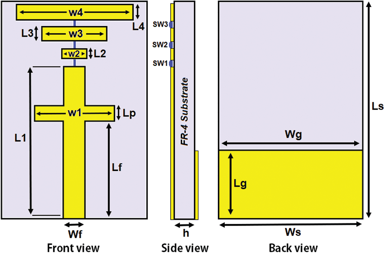
Figure 1: The geometry of proposed antenna
Table 1: Dimensions of proposed antenna
The effective resonant lengths for intended frequencies are calculated using transmission line model theory [30]. The effective length of the antenna corresponding to the respective resonant bands are one quarter of the guided wavelength (i.e.,
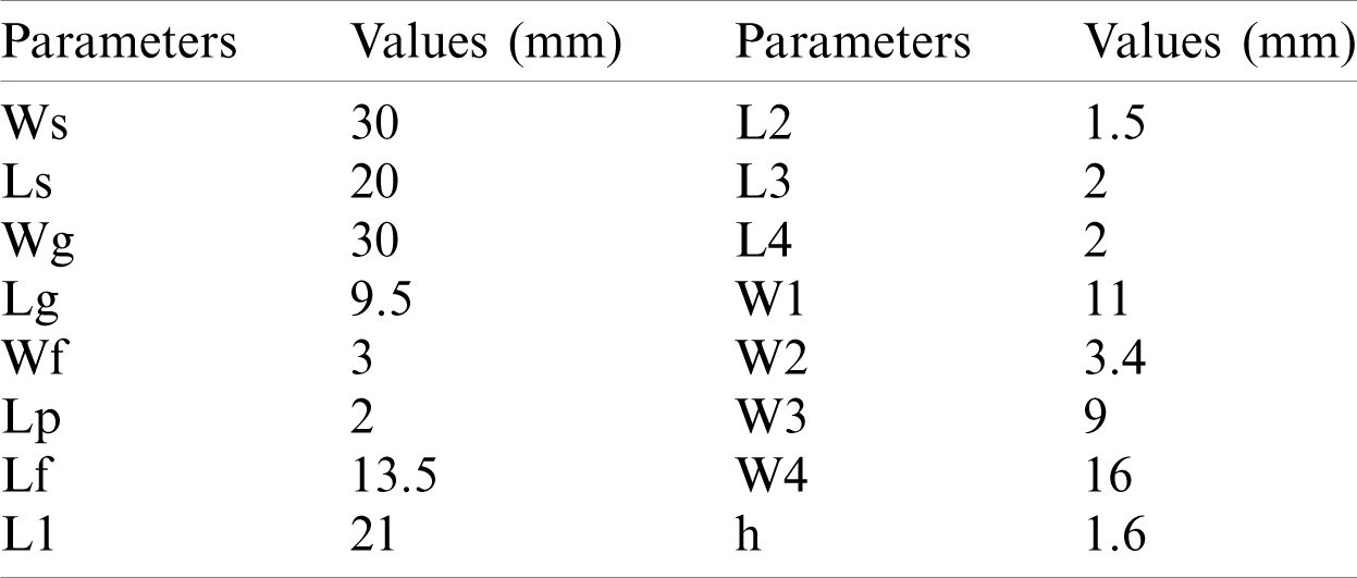
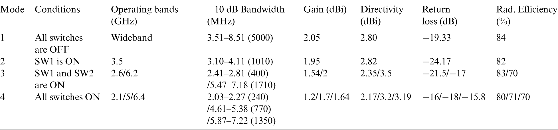
In proposed antenna frequency reconfigurability is achieved by changing the ON and OFF states of each pin diode that offers an open and short circuit behavior between radiating patches. The presented antenna has four operating modes, each have unique scheme of resonant frequencies. In Mode 1 (SW1 to
Table 2: Conditions of the pin diodes for various resonant bands
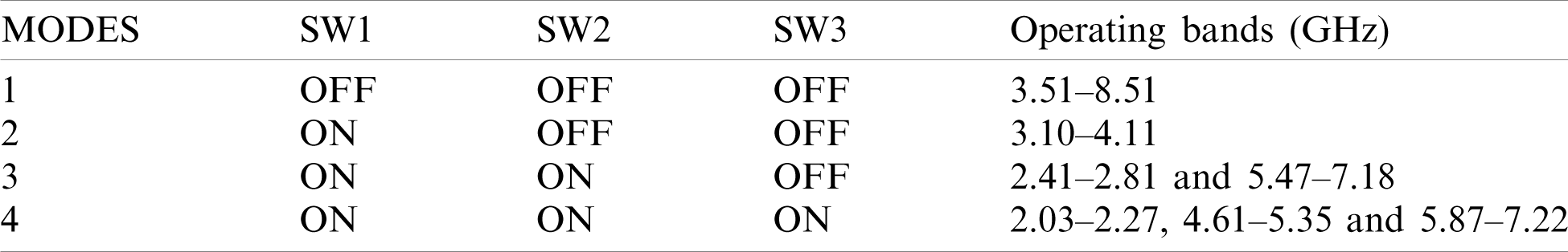
For switching purpose four pin diodes (SMP1345-079LF) are used, as they behave like a variable resistor in the radio frequency (RF) range. These pin diodes provide open and the short circuit behavior at their respective insertion positions, thus vary the effective resonant length of the antenna and hence result in reconfiguration of antenna’s operating frequency. The equivalent circuits for both ON and OFF states of a pin diode switches are shown in the Fig. 2. For ON state it is simply an RL series circuit, having a low value resistor “RL” and an inductor “L”. In OFF state it is equivalent to an RLC circuit, having inductor “L” in parallel with a high value resistor “Rh” and a capacitor “C”. Pin diode of model Skyworks SMP1345-079LF are used in this work. According to its datasheet it has been modeled in CST as
Figure 2: Pin diode model and its equivalent circuits for ON and OFF states
The evolution of the proposed antenna’s design involves several steps as depicted in the Fig. 3. All steps along with their return loss characteristic are illustrated in Figs. 3–6. For achieving Mode 1, a monopole antenna excited with a microstrip feedline was designed to cover the 5.8–8.2 GHz frequency band. For achieving the lower frequency bands the length L1 was increased from 17 to 21 mm. To achieve the better bandwidth and enhanced impedance matching for the intended resonant bands, the parameter W1 was increased, from 3 to 11 mm as shown in Fig. 4.
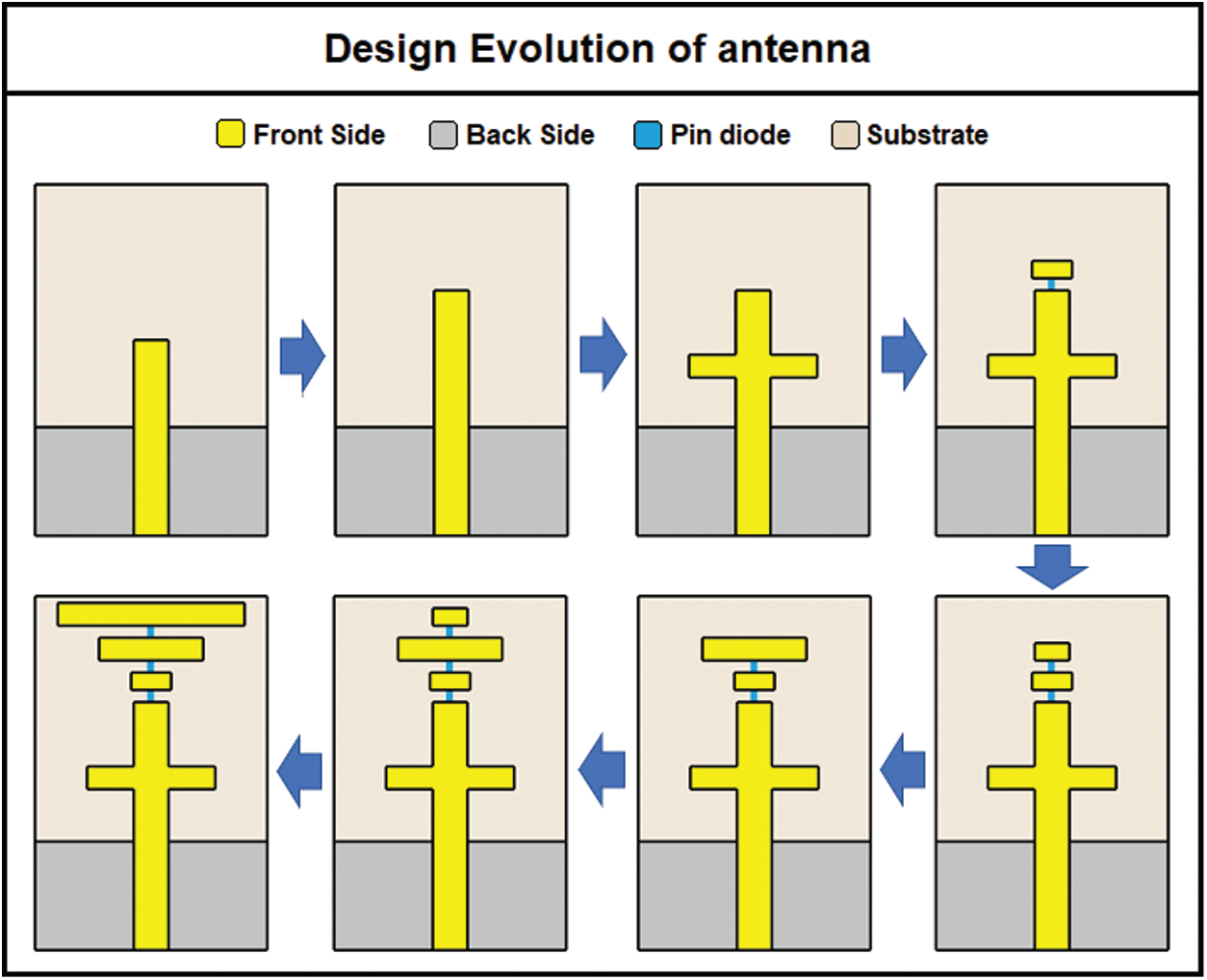
Figure 3: The evolution map highlighting various design stages of the proposed antenna
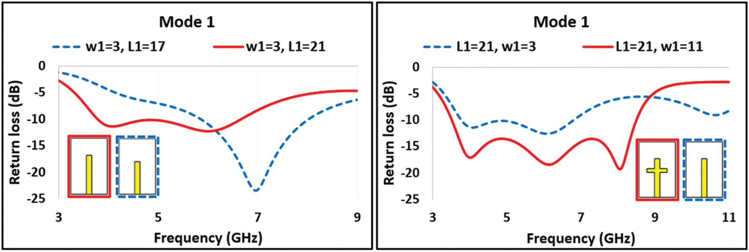
Figure 4: Design evolution of Mode 1 of proposed antenna
For Mode2, a parasitic patch was introduced, connected in cascade with the primary radiator. It may be noted that the value of W1 was kept constant in this mode, equal to 11 mm. At width
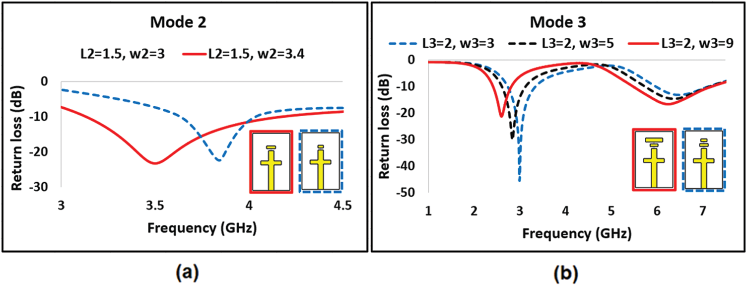
Figure 5: Design evolution of Mode 2 and Mode 3
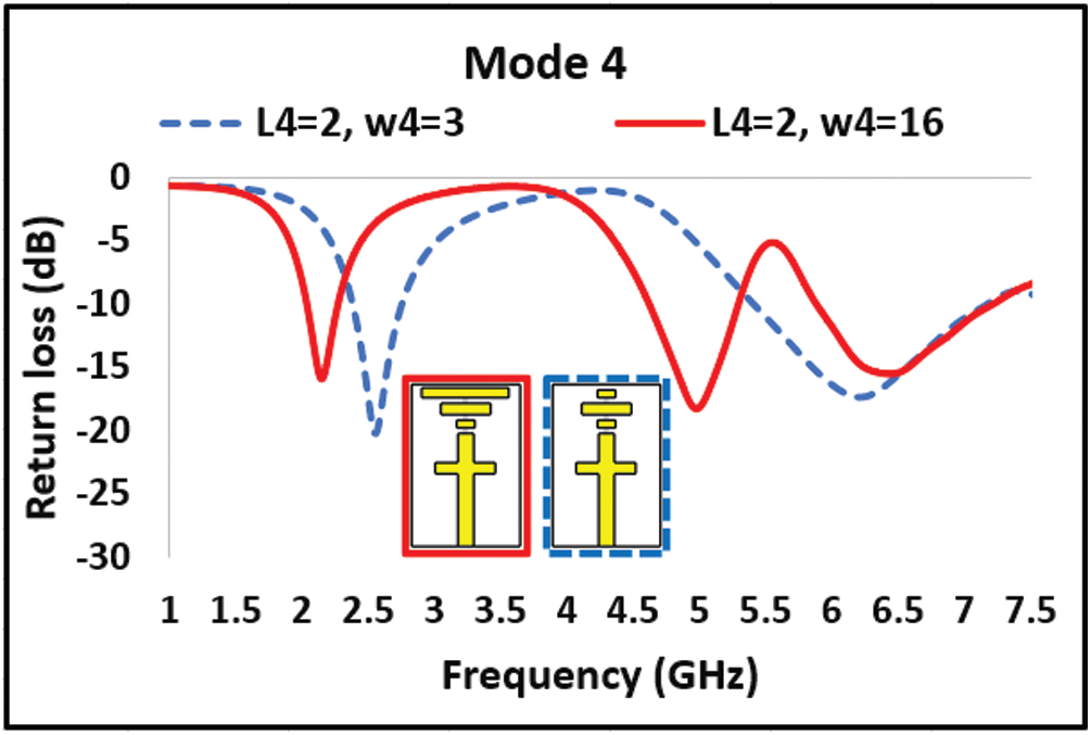
Figure 6: Design evolution of Mode 4
The proposed structure is designed and analyzed using Computer Simulation Technology microwave studio (CST MWS). To excite the radiating structure, a waveguide port of standard dimensions is assigned. The performance parameters i.e., return loss, gain, surface current plots are obtained by using the standard boundary conditions in CST microwave studio. The simulated results are experimentally validated in the antenna measurement facility located at National University of Science and Technology (NUST) Islamabad. The experimental setup to measure the radiation pattern of the proposed antenna in mode 1 is depicted in Fig. 7.
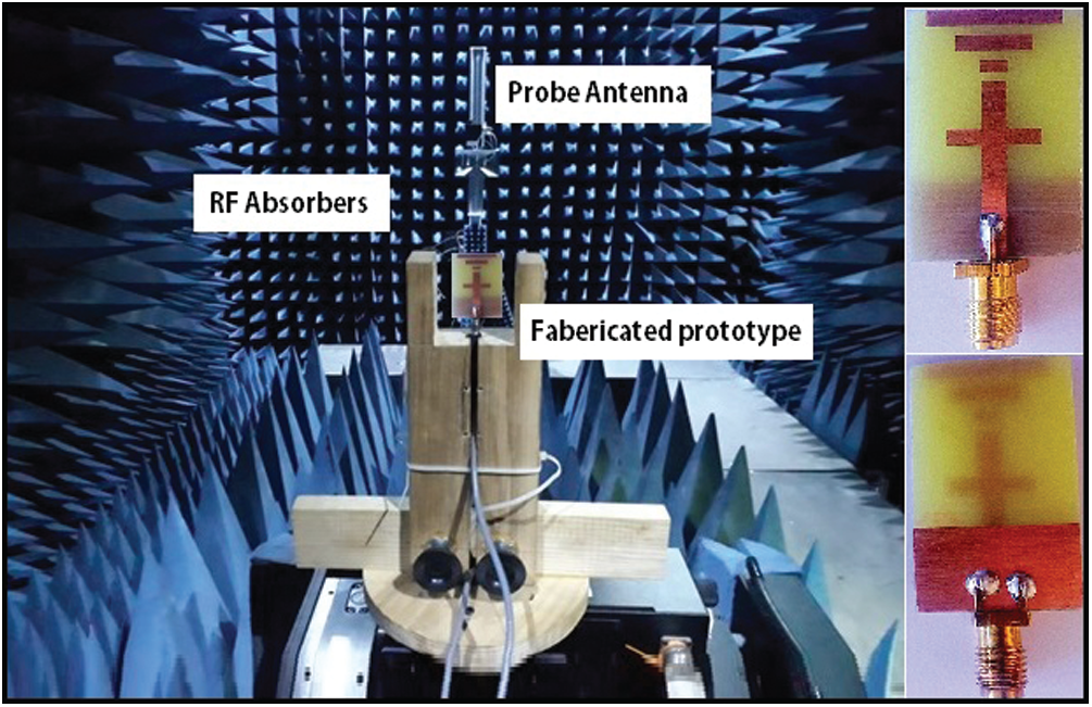
Figure 7: Setup for measuring radiation pattern of the proposed antenna in Mode 1
The simulated return loss of all modes of the proposed antenna are depicted in Fig. 8. When all switches (SW1 to SW3) are OFF, the proposed antenna operates in MODE 1, covering 3.51–8.51 GHz band with maximum return loss of −19.33 dB at 8 GHz. In MODE 2 (When SW 1 is ON), the presented antenna resonates at 3.5 GHz with return loss of −24.17 and −10 dB bandwidth of 1010 MHz (3.10–4.11). In MODE 3 when two switches (SW1, SW2) are ON and the SW3 is OFF, the proposed antenna operates at two different bands i.e., 2.6 and 6.2 GHz with a return loss of −21.5, −17 and −10 dB bandwidth of 400 MHz (2.41–2.81 GHz) and 1710 MHz (5.47–7.18 GHz), respectively. When all switches (SW1 to SW3) are ON, the antenna switch to its MODE 4 and operates at 2.1, 5, and 6.4 GHz with return loss of −16, −18, −15.8 dB and −10 dB bandwidth of 240 MHz (2.03–2.27 GHz), 740 MHz (4.61–5.35 GHz) and 1350 MHz (5.87–7.22 GHz), respectively at the operating frequencies.
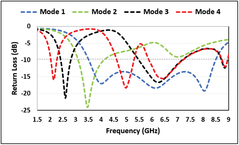
Figure 8: Return loss for all operating modes
The simulated and measured return loss of each mode is compared in Fig. 9. The comparison shows a good agreement between measured and simulated results. The VSWR of less than 1.5 is observed for all resonant bands, which indicates optimum driving-point impedance matching of the antenna, as depicted in Fig. 10.
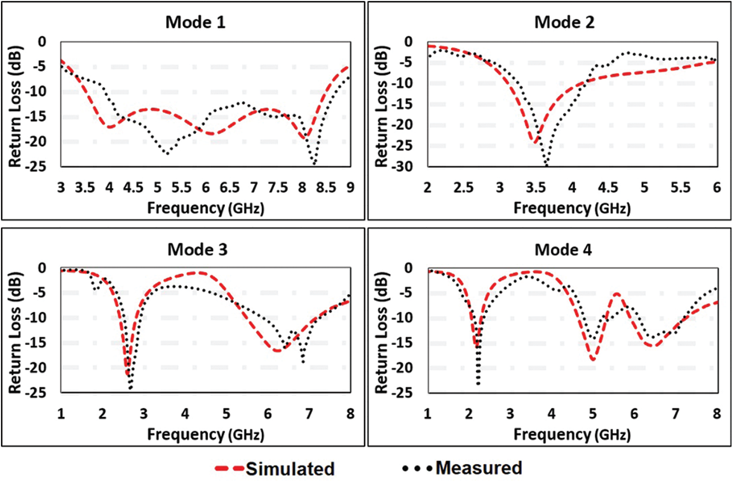
Figure 9: Comparison of simulated and measured return loss
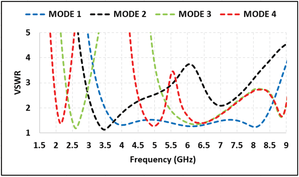
Figure 10: VSWR of proposed antenna at various operating modes
3.2 Far Field Radiation Pattern
In MODE 1, proposed antenna operates at 3.51–8.51 GHz band with a simulated peak gain and radiation efficiency of 2.5 dBi and 84%, respectively. In MODE 2, a central frequency of 3.5 GHz has been achieved with peak gain and radiation efficiency of 1.95 dBi and 82%, respectively. A dual band is achieved in MODE 3 with gain of 1.54 and 2 dBi and radiation efficiencies of 83% and 70% at 2.6 and 6.2 GHz, respectively. The antenna operates at 2.1, 5 and 6.4 GHz in MODE 4, with peak gains of 1.2, 1.7 and 1.64 dBi and radiation efficiencies of 80%, 71% and 70%, respectively.
The comparison of simulated and measured gain of proposed antenna is depicted in Fig. 11 showing that the measured gains are in a good agreement with the simulated ones. It is worth mentioning that the antenna gives optimum values of average gain, i.e., 2.05 dBi in mode 1, 1.87 dBi in mode 2, 1.4–1.75 dBi in mode 3, 1.05–1.56 dBi in mode 4.
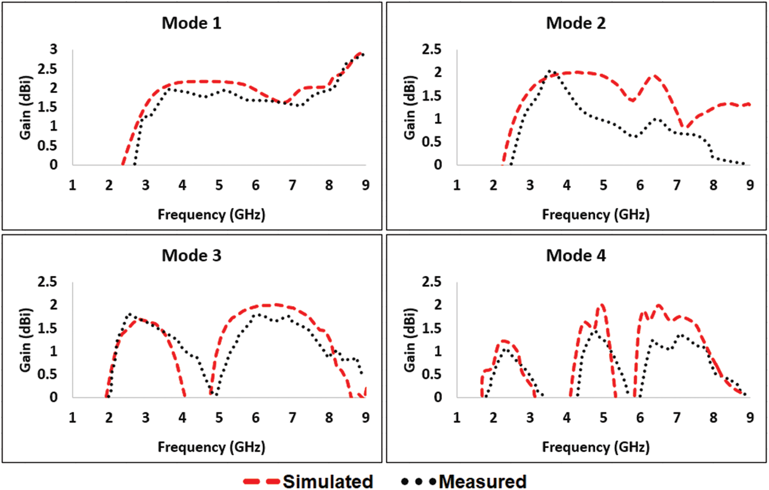
Figure 11: Comparison of simulated and measured gain
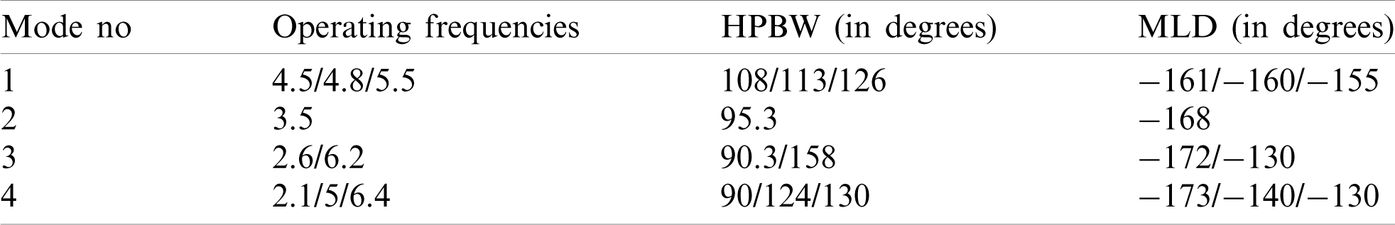
The simulated and measured radiation pattern of the antenna in both E-and H-plane at the operating frequency bands, are compared in Fig. 12. The shape of the radiation pattern in the E-plane, resembles the figure-of-eight at frequencies of 2.1, 2.6, 3.5 GHz. The radiation properties of the antenna in the H-plane are predominantly Omni-directional in nature in most of the frequency bands. The half power beamwidth (HPBW) and main lobe direction (MLD) were deduced from the E-plane radiation pattern of the antenna in all resonant modes, and the same are summarized in Tab. 3.
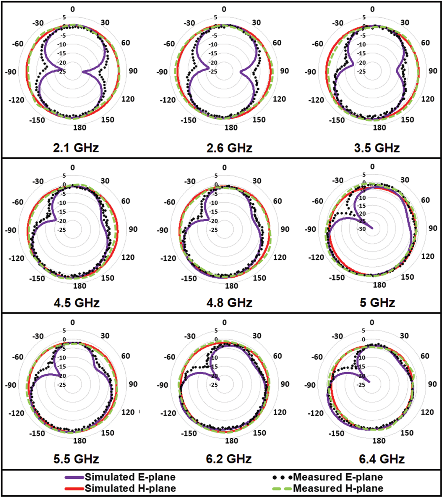
Figure 12: Comparison of simulated and measured radiation pattern in both principal planes
Table 3: Summary of half power beamwidth and main lobe direction
The simulated co-and cross-polar radiation patterns for both E-plane (y-z) and H-plane (x-z) are presented in Fig. 13. It is evident from the results that in the co-polarization state, the antenna radiates adequately in both E-and H-planes. While, in cross-polarization state, the antenna gain is predominately negative and hence the radiation is extremely poor in both principal planes. For further clarity about the radiation properties of the antenna, the three-dimensional gain plots are portrayed at the resonant frequencies in Fig. 14.
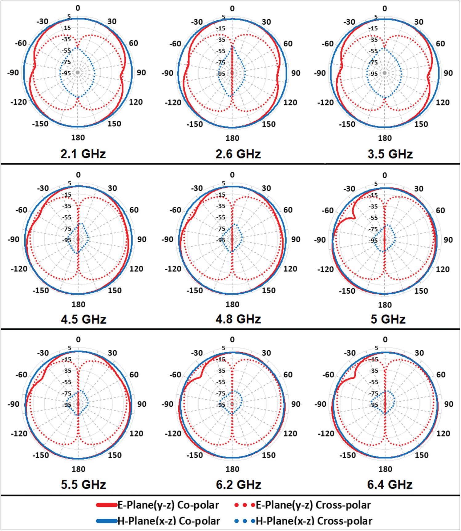
Figure 13: Co-and cross-polar radiation pattern for both principal planes
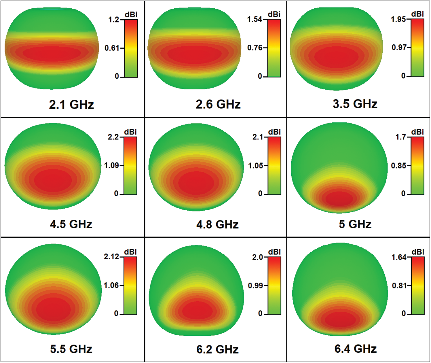
Figure 14: The three-dimensional plots of gain pattern
The surface current distribution on the radiating structure of the antenna at different frequency bands is shown in Fig. 15. For Mode 1, antenna operates at a wideband of 3.51–8.51 GHz, the density of the surface currents is higher on the lower side of the feedline, which is contributing to radiation at 5.5, 4.8, 4.5GHz, low concentration for high frequency and more concentrated surface currents are observed for lower frequencies bands. In Mode 2, the surface currents indicate an increase in the contributing resonant length, thus operation shifts to 3.5 GHz. In Mode 3 dual band operations (i.e., 2.6 and 6.2 GHz) are achieved, the surface currents indicate the dominant contribution of larger portion of radiator for lower bands and smaller portion of radiator for the upper bands. In Mode 4, triple band (i.e., 2.1, 5 and 6.4 GHz) operation is achieved, the higher surface current density along the entire length of the radiator indicate that the whole metallic radiator is contributing to radiation in the lower frequency band (i.e., 2.1 GHz). It is worth mentioning that relatively smaller segments of the radiator are contributing to radiation at the upper bands (5.5 and 6.4 GHz). These surface currents indicate that the contributing resonant length for respective frequency decreases as resonant frequency increases, thus proves the inverse relation of frequency with resonant length. Performance matrices of proposed antenna are summarized in Tab. 4. The power consumption by the parasitic resistance of the pin diodes and as well as the power loss in the dielectric substrate were analyzed for each operating frequency. The average power consumption or loss contributed by the pin diodes and dielectric substrate is 0.023 and 0.031 w, respectively.
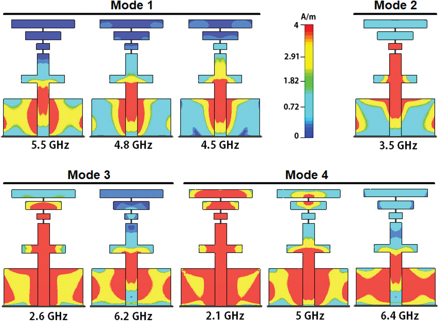
Figure 15: Surface currents plots of antenna at various modes
Table 4: Summary of the antenna’s performance
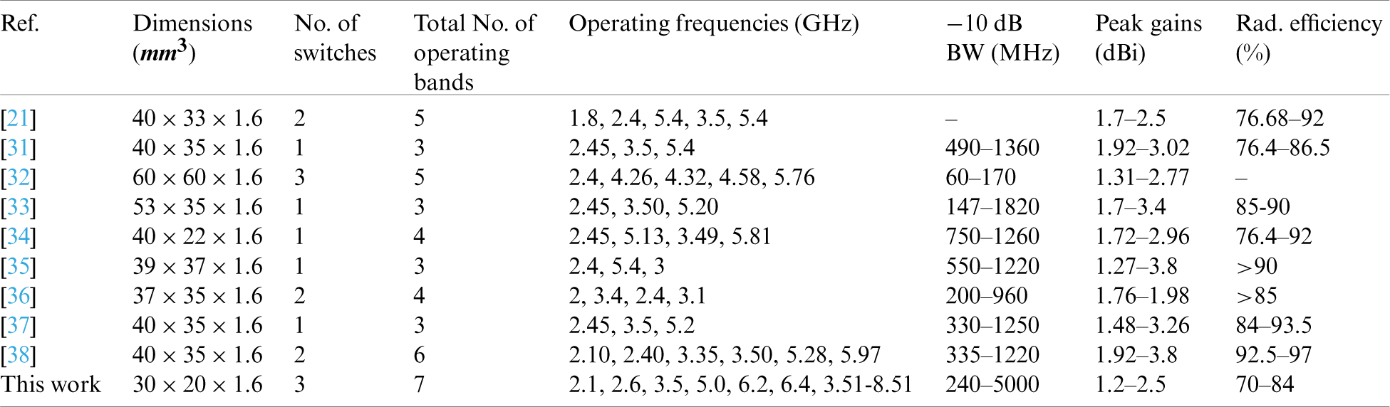
In terms of size, the proposed antenna is more compact than all the antennas reported in the comparison table. The proposed antenna has impedance bandwidth (BW) ranges 240–5000 MHz which offers larger bandwidth than antennas designed in [31–38]. The comparison is given in Tab. 5.
Table 5: Proposed antenna’s comparison with other reported works
A frequency reconfigurable antenna has been designed, simulated, and experimentally validated in this paper. The proposed antenna is reconfigured depending on the ON and OFF states of the pin diode switches. When all the switches are OFF, the antenna covers a wide band of 3.51 to 8.51 GHz. Antenna operates at 3.5 GHz when only SW1 is ON. The prototype works in dual band mode, resonating at 2.6 GHz and 6.2 GHz, when SW1 and SW2 are ON. Triple band (2.1, 5 and 6.4 GHz) functionality is realized when all the switches are kept in ON condition. The proposed antenna has many advantages like compact size, low cost, light weight and easy of fabrication and supports sub-6 GHz 5G bands (2.1, 2.6, 3.5 and 5 GHz) with an extended application for wireless local area networks, the 6 GHz fixed satellite services as well as IoT enabled wireless terminal and systems in smart cities.
Funding Statement: This research was supported by SUT Research and Development Fund.
Conflicts of Interest: The authors declare that they have no conflicts of interest to report regarding the present study.
1. M. H. Alsharif and R. Nordin, “Evolution towards fifth generation (5G) wireless networks: Current trends and challenges in the deployment of millimetre wave, massive MIMO, and small cells,” Telecommunication Systems, vol. 64, no. 4, pp. 617–637, 2017. [Google Scholar]
2. J. Costantine, Y. Tawk, S. E. Barbin and C. G. Christodoulou, “Reconfigurable antennas: Design and applications,” Proc. of the IEEE, vol. 103, no. 3, pp. 424–437, 2015. [Google Scholar]
3. I. F. Akyildiz, W. Y. Lee, M. C. Vuran and S. Mohanty, “Next generation/dynamic spectrum access/cognitive radio wireless networks: A survey,” Computer Networks, vol. 50, no. 13, pp. 2127–2159, 2006. [Google Scholar]
4. S. Nikolaou, R. Bairavasubramanian, C. Lugo, I. Carrasquillo, D. C. Thompson et al., “Pattern and frequency reconfigurable annular slot antenna using PIN diodes,” IEEE Transactions on Antennas and Propagation, vol. 54, no. 2, pp. 439–448, 2006. [Google Scholar]
5. M. N. Osman, M. K. A. Rahim, P. Gardner, M. R. Hamid, M. F. M. Yusoff et al., “An electronically reconfigurable patch antenna design for polarization diversity with fixed resonant frequency,” Radioengineering, vol. 24, no. 1, pp. 45–53, 2015. [Google Scholar]
6. M. Kelley, C. Koo, H. McQuilken, B. Lawrence, S. Li et al., “Frequency reconfigurable patch antenna using liquid metal as switching mechanism,” Electronics Letters, vol. 49, no. 22, pp. 1370–1137, 2013. [Google Scholar]
7. H. A. Majid, M. K. A. Rahim, M. R. Hamid, N. A. Murad and M. F. Ismail, “Frequency-reconfigurable microstrip patch-slot antenna,” IEEE Antennas and Wireless Propagation Letters, vol. 12, pp. 218–220, 2013. [Google Scholar]
8. L. Ge and K. M. Luk, “Frequency-reconfigurable low-profile circular monopolar patch antenna,” IEEE Transactions on Antennas and Propagation, vol. 62, no. 7, pp. 3443–3449, 2014. [Google Scholar]
9. I. Kim and Y. Rahmat-Samii, “RF MEMS switchable slot patch antenna integrated with bias network,” IEEE Transactions on Antennas and Propagation, vol. 59, no. 12, pp. 4811–4815, 2011. [Google Scholar]
10. C. Wang, B. Yuan, W. Shi and J. Mao, “Low-profile broadband plasma antenna for naval communications in VHF and UHF Bands,” IEEE Transactions on Antennas and Propagation, vol. 68, no. 6, pp. 4271–4282, 2020. [Google Scholar]
11. I. D. Feliciano, A. C. Sodré Jr, J. S. R. Páez, R. Puerta, J. J. V. Olmos et al., “Photonics-assisted wireless link based on mm-wave reconfigurable antennas,” IET Microwaves, Antennas & Propagation, vol. 11, no. 14, pp. 2071–2076, 2017. [Google Scholar]
12. M. S. Alam and A. M. Abbosh, “Beam-steerable planar antenna using circular disc and four PIN-controlled tapered stubs for WiMAX and WLAN applications,” IEEE Antennas and Wireless Propagation Letters, vol. 15, pp. 980–983, 2015. [Google Scholar]
13. X. Zhao, S. Riaz and S. Geng, “A reconfigurable MIMO/UWB MIMO antenna for cognitive radio applications,” IEEE Access, vol. 7, pp. 46739–46747, 2019. [Google Scholar]
14. R. K. Verma, A. Kumar and R. L. Yadava, “Compact multiband CPW fed sub 6 GHz frequency reconfigurable antenna for 5G and specific UWB applications,” Journal of Communications, vol. 15, no. 4, pp. 345–349, 2020. [Google Scholar]
15. G. Jin, C. Deng, J. Yang, Y. Xu and S. Liao, “A new differentially-fed frequency reconfigurable antenna for WLAN and Sub-6 GHz 5G applications,” IEEE Access, vol. 7, pp. 56539–56546, 2019. [Google Scholar]
16. M. T. Khan, M. T. Jilani, A. M. Khan, F. Hafeez and A. K. Memon, “Effects of defected ground structure slot tuning on frequency and circuit parameters of bandpass filter,” Journal of Optoelectronics and Advanced Materials, vol. 20, pp. 479–485, 2018. [Google Scholar]
17. A. Iqbal, A. Smida, L. F. Abdulrazak, O. A. Saraereh, N. K. Mallat et al., “Low-profile frequency reconfigurable antenna for heterogeneous wireless systems,” Electronics, vol. 8, no. 9, pp. 976, 2019. [Google Scholar]
18. I. A. Shah, S. Hayat, A. Basir, M. Zada, S. A. A. Shah et al., “Design and analysis of a hexa-band frequency reconfigurable antenna for wireless communication,” AEU-International Journal of Electronics and Communications, vol. 98, no. 1, pp. 80–88, 2019. [Google Scholar]
19. A. Desai, R. Patel, T. Upadhyaya, H. Kaushal and V. Dhasarathan, “Multiband inverted E and U shaped compact antenna for digital broadcasting, wireless, and sub 6 GHz 5G applications,” AEU-International Journal of Electronics and Communications, vol. 123, no. 1, pp. 153296, 2020. [Google Scholar]
20. Y. K. Park and Y. Sung, “A reconfigurable antenna for quad-band mobile handset applications,” IEEE Transactions on Antennas and Propagation, vol. 60, no. 6, pp. 3003–3006, 2012. [Google Scholar]
21. S. Hayat, I. A. Shah, I. Khan, I. Alam, S. Ullah et al., “Design of tetra-band frequency reconfigurable antenna for portable wireless applications,” in Int. Conf. on Intelligent Systems Engineering, Islamabad, Pakistan, pp. 15–17, 2016. [Google Scholar]
22. S. S. Bharadwaj, D. Sipal, D. Yadav and S. K. Koul, “A compact tri-band frequency reconfigurable antenna for LTE/WI-FI/ITS application,” Progress in Electromagnetics Research, vol. 91, pp. 59–67, 2020. [Google Scholar]
23. Y. B. Chaouche, I. Messaoudene, I. Benmabrouk, M. Nedil and F. Bouttout, “Compact coplanar waveguide-fed reconfigurable fractal antenna for switchable multiband systems,” IET Microwaves, Antennas & Propagation, vol. 13, no. 1, pp. 1–8, 2018. [Google Scholar]
24. F. A. Asadallah, J. Costantine and Y. Tawk, “A multiband compact reconfigurable PIFA based on nested slots,” IEEE Antennas and Wireless Propagation Letters, vol. 17, no. 2, pp. 331–334, 2018. [Google Scholar]
25. A. Ghaffar, X. J. Li, B. C. Seet, W. A. Awan and N. Hussain, “Compact multiband frequency reconfigurable antenna for 5G communications,” in 29th Int. Telecommunication Networks and Applications Conf., Auckland, New Zealand, pp. 1–3, 2019. [Google Scholar]
26. G. Jin, C. Deng, Y. Xu, J. Yang and S. Liao, “Differential frequency reconfigurable antenna based on dipoles for sub-6 GHz 5G and WLAN applications,” IEEE AWPL Antennas and Wireless Propagation Letters, vol. 19, no. 3, pp. 472–476, 2020. [Google Scholar]
27. A. Shahgholi, G. Moradi and A. Abdipour, “Low-profile frequency-reconfigurable LTE-CRLH antenna for smartphones,” IEEE Access, vol. 8, pp. 26487–26494, 2020. [Google Scholar]
28. N. Hussain, W. A. Awan, S. I. Naqvi, A. Ghaffar, A. Zaidi et al., “A compact flexible frequency reconfigurable antenna for heterogeneous applications,” IEEE Access, vol. 8, pp. 173298–173307, 2020. [Google Scholar]
29. A. Ghaffar, X. J. Li, W. A. Awan and N. Hussain, “A compact multiband multi-mode frequency reconfigurable antenna for portable devices,” in 2020 Int. Conf. on UK-China Emerging Technologies, Glasgow, UK, pp. 1–4, 2020. [Google Scholar]
30. C. A. Balanis, Antenna Theory: Analysis and Design, 4th ed. New Jersey, United States: John Wiley & Sons, 2016. [Google Scholar]
31. S. A. A. Shah, M. F. Khan, S. Ullah and J. A. Flint, “Design of a multi-band frequency reconfigurable planar monopole antenna using truncated ground plane for Wi-Fi, WLAN and WiMAX applications,” in 2014 Int. Conf. on Open-Source Systems & Technologies, Lahore, Pakistan, pp. 151–155, 2014. [Google Scholar]
32. B. Saikia, P. Dutta and K. Borah, “Design of a frequency reconfigurable microstrip patch antenna for multiband applications,” in Proc. of the 5th Int. Conf. on Computers & Management Skills, Arunachal Pradesh, India, pp. 15–16, 2019. [Google Scholar]
33. S. Ullah, S. Hayat, A. Umar, U. Ali, F. A. Tahir et al., “Design, fabrication and measurement of triple band frequency reconfigurable antennas for portable wireless communications,” AEU-International Journal of Electronics and Communications, vol. 81, pp. 236–242, 2017. [Google Scholar]
34. S. A. A. Shah, M. F. Khan, S. Ullah, A. Basir, U. Ali et al., “Design and measurement of planar monopole antennas for multi-band wireless applications,” IETE Journal of Research, vol. 63, no. 2, pp. 194–204, 2017. [Google Scholar]
35. A. Iqbal, S. Ullah, U. Naeem, A. Basir and U. Ali, “Design, fabrication and measurement of a compact, frequency reconfigurable, modified T-shape planar antenna for portable applications,” Journal of Electrical Engineering and Technology, vol. 12, no. 4, pp. 1611–1618, 2017. [Google Scholar]
36. S. Ullah, I. Ahmad, Y. Raheem, S. Ullah, S. T. Ahmad et al., “Hexagonal shaped CPW feed based frequency reconfigurable antenna for WLAN and Sub-6 GHz 5G applications,” in Int. Conf. on Emerging Trends in Smart Technologies, Karachi, Pakistan, pp. 26–27, 2020. [Google Scholar]
37. I. A. Shah, S. Hayat, I. Khan, I. Alam, S. Ullah et al., “A compact, tri-band and 9-shape reconfigurable antenna for WiFi, WiMAX and WLAN applications,” International Journal of Wireless and Microwave Technologies, vol. 6, no. 5, pp. 45–53, 2016. [Google Scholar]
38. S. Ullah, A. Shaheen, B. A. Khan and J. A. Flint, “A multi-band switchable antenna for Wi-Fi, 3G advanced, WiMAX, and WLAN wireless applications,” International Journal of Microwave and Wireless Technologies, vol. 10, no. 8, pp. 991–997, 2018. [Google Scholar]
 | This work is licensed under a Creative Commons Attribution 4.0 International License, which permits unrestricted use, distribution, and reproduction in any medium, provided the original work is properly cited. |