DOI:10.32604/cmc.2021.017575
| Computers, Materials & Continua DOI:10.32604/cmc.2021.017575 | |
| Article |
An Optimized SW/HW AVMF Design Based on High-Level Synthesis Flow for Color Images
1Department of Electrical Engineering, Jouf University, Sakaka, Aljouf, Saudi Arabia
2LETI (E.N.I.S.), University of Sfax, Sfax, Tunisia
*Corresponding Author: Ahmed Ben Atitallah. Email: abenatitallah@ju.edu.sa
Received: 28 January 2021; Accepted: 04 March 2021
Abstract: In this paper, a software/hardware High-level Synthesis (HLS) design is proposed to compute the Adaptive Vector Median Filter (AVMF) in real-time. In fact, this filter is known by its excellent impulsive noise suppression and chromaticity conservation. The software (SW) study of this filter demonstrates that its implementation is too complex. The purpose of this work is to study the impact of using an HLS tool to design ideal floating-point and optimized fixed-point hardware (HW) architectures for the AVMF filter using square root function (ideal HW) and ROM memory (optimized HW), respectively, to select the best HLS architectures and to design an efficient HLS software/hardware (SW/HW) embedded AVMF design to achieve a trade-off between the processing time, power consumption and hardware cost. For that purpose, some approximations using ROM memory were proposed to perform the square root and develop a fixed-point AVMF algorithm. After that, the best solution generated for each HLS design was integrated in the SW/HW environment and evaluated under ZC702 FPGA platform. The experimental results showed a reduction of about 65% and 98% in both the power consumption and processing time for the ideal SW/HW implementation relative to the ideal SW implementation for an AVMF filter with the same image quality, respectively. Moreover, the power consumption and processing time of the optimized SW/HW are 70% and 97% less than the optimized SW implementation, respectively. In addition, the Look Up Table (LUTs) percentage, power consumption and processing time used by the optimized SW/HW design are improved by nearly 45%, 18% and 61% compared the ideal SW/HW design, respectively, with slight decrease in the image quality.
Keywords: AVMF filter; SW/HW design; HLS flow; ZC702 FPGA platform
The contamination of the color images by “salt and pepper” impulse noise presents the most common problem in image processing. In fact, starting from communication field to the field of security and health, image processing has a vital role to play. Therefore, it is very important to determine the corruption produced by this noise and ameliorate the quality of the image before further processing.
Image filtering is the most important stage in the image processing operation [1,2]. It helps to suppress the noise and to restore and ameliorate the image quality. Image filtering is used in a vast array of applications such as satellite images where the noise can affect the image quality through the capture and transmission processes [3]. Thus, it is vital to eliminate the noise from satellite imagery because it is used in several vital fields such as security, water bodies, changing lands and planet health [4]. Besides, in the medical profession, images can contain “salt and pepper” noise, which affects image quality, especially in ultrasound imaging and Magnetic Resonance Imaging (MRI) [5]. It is, hence, critical to eliminate noise from medical images as crucial information may be affected.
The earliest filters were based on linear approaches which cannot take account of the non-linearity of human vision [6] and cannot be suitable for the non-linearities of transmission channels. For that, the non-linear filters are appropriate to the digital color images. Many non-linear filters have been proposed in the literature such as the Vector Median Filter (VMF) [7], the Adaptive Vector Median Filter (AVMF) [8], the Vector Median Rational Hybrid Filter (VMRHF) [9], etc.
Many researchers have noted the time consuming and the high complexity of non-linear filters [10,11]. However, to reduce this complexity, researchers have adopted hardware acceleration as a solution. In fact, Trivedi et al. [12] propose a hardware implementation of the median filtering on Field-Programmable Gate-Array (FPGA) which consumes less power and less hardware area. Hu et al. [13] propose two hardware architectures to implement the median filtering counting standard and multi-level median filters. In [14], an optimized hardware architecture based on systolic array is developed to implement median filtering. This architecture uses the pipeline structure which requires seven clock cycles to determine the median value. Lee et al. [15] detail a
But these hardware architectures miss the flexibility of design updating and take more development time. Indeed, the development and implementation of these architectures are done by Low-Level Synthesis (LLS) using hardware description language (HDL) on an FPGA circuit. With LLS design, it is possible to adjust the Register Transfer Level (RTL) description to give a very great, optimized netlist. However, producing such an RTL description requires a lot of effort and time to describe the operations of each low-level circuit and, especially for complex applications [17,18]. Nevertheless, designing a complex system is only possible for hardware designers who have specific knowledge and skills. Therefore, there is a real need to raise the design space abstraction level from LLS to High-Level Synthesis (HLS) [19,20] in order to reduce the FPGA design complexity. In fact, HLS allows designers to formalize algorithms using software high-level language (systemC, C/C++ , etc.) and synthesizes them via the HLS tool to form a behavioral and structural of the RTL hardware description. In this context, several academic and commercial HLS tools are developed such as Xilinx Vivado HLS, Intel OpenCL [21], Catapult-C [22], and ROCCC [23]. However, without any expertise and skills in hardware design, designers can develop and generate automatically from high-level language a complex hardware design which permits designers to explore and simulate a large design space in the shortest of times, identify design performances (power consumption, processing time and hardware cost) and eliminate the source of many design errors. Unfortunately, to design an optimized and high performant RTL circuit with HLS tools, the code should be restructured in a specific style. Without such restructuring, the HLS tools can still generate an RTL circuit but with poor performance [24].
Given this context, our goal in this work is to use HLS flow to design various hardware architectures for the AVMF filter and integrate these architectures as intellectual property (IPs) blocks with Hardcore ARM processor on Xilinx Zynq FPGA in order to design an efficient software/hardware (SW/HW) embedded system. The SW/HW design should reduce this filter’s complexity and power consumption as well as speed up the execution time. However, HW solution is used for performance (processing speed and power consumption). In contrast, SW solution is used for design flexibility [25,26].
The remainder of the paper is organized as follows. In Section 2 below an overview of the AVMF filter is presented. The description of Vivado HLS tool and directives are given in Section 3. The proposed HLS AVMF designs are described in Section 4. Section 5 discusses the experimental results in terms of hardware cost, power consumption and processing time of the SW/HW AVMF implementation on ZC702 platform. Finally, conclusion is given in Section 6.
In [8], the author presents an Adaptive Vector Median Filter (AVMF) which is based on the VMF filter. It is enhanced by using a threshold to detect the probability of the pixel to be noisy as shown in Fig. 1.

Figure 1: AVMF filter algorithm
We define by
where
The output yAVMF of the AVMF is expressed in (2) below:
where the vector
The vector
where
The approximation presented in (5) determines the mean distance between the vector median and the different pixels held in V. In this equation,
The purpose of HLS methodology is to simplify and accelerate the hardware implementation specially for FPGA circuits. For that, an HLS tool is developed by Xilinx to help engineers to rapidly implement algorithms on the FPGA with gains in resource, power, and performance. This tool is called Vivado HLS which gives a design environment to interpret, analyze, optimize, and transform a software language like C/C++ to RTL design. This design is synthesized and implemented for Xilinx FPGA. Indeed, with the Vivado HLS tool, it is possible to apply different optimizations to increase the hardware design performances by using several directives such as pipelining, loop unrolling, resource, etc. Some optimizations lead to decreasing the hardware area by applying the ALLOCATION directive. This directive can minimize the number of resources using in design by sharing resource between several functions. Moreover, RESOURCE directive can be used to replace vectors and arrays by specific memory blocks (BRAMs). But, to raise the data rate and achieve a higher throughput, the UNROLL or PIPELINE directives can be used. In this case, by unrolling loops, several hardware blocks are built in parallel to operate the loop iterations in parallel. Otherwise, the PIPELINE directive performs pipelining to reach higher throughput. In fact, the pipeline technique permits the loop iteration to begin before the completion of its predecessor. For that, the data dependencies should be satisfied. Furthermore, the ARRAY PARTITION directive divides the large memory into individual registers or multiple smaller memory blocks for parallel data accesses. However, these optimizations lead to an excessive use of FPGA resources. For that, the level of pipelining or parallelism should be customized.
With Vivado HLS tool, some steps should be followed to generate an RTL description. In Step 1, the C/C++ code should be written in a specific style to permit the HLS tool to create an optimized RTL description. In Step 2, the source code is explored to extract the control path and dataflow. In Step 3, a various specific directive is applied for each algorithm for better hardware optimization. In the last step, the Export RTL tool is used to export as an IP module the created RTL design to the Xilinx Vivado tool in order to generate the bitstream file.
4 HLS Architecture of the AVMF Filter
The developed AVMF C code is given as input to the Vivado HLS tool 18.1 in order to generate a hardware architecture for AVMF algorithm. The generated architecture is illustrated in Fig. 2. This architecture is optimized to reconstruct the filtered color image in minimum of clock cycles. In fact, to optimize the load of pixels, tree lines of image are sent in parallel to the AVMF coprocessor. In order to form a
From Fig. 2, we can see that the EDs are implemented based on Eq. (6) and computed by using 81 loop iterations. In fact, the loop 1 is used nine times to accumulate nine EDs
The bottleneck of this architecture is the implementation of the square root (SQRT) which is used to calculate the EDs for the AVMF filter and the floating-point values. Thus, the purpose of this work is to generate two HLS architectures for the AVMF filter. The first architecture is based on the SQRT function. The second architecture is based on the approximation of the SQRT function in order to use the fixed-point values only and reduce the hardware complexity. Our main goal is to design floating-point and fixed-point architectures using Vivado HLS tool and compares the power consumption, the processing time and the area cost of the designed architectures.

Figure 2: AVMF coprocessor
4.1 HLS Floating-Point AVMF Design
Several designs are generated from AVMF C floating-point code. These designs are generated by adding incrementally specific directives through the Vivado HLS tool and synthesized for Xilinx XC7Z020 FPGA. After that, we are compared the performance in terms of number of clock cycles and hardware resources (LUTs, FFs, BRAMs and DSPs).
#Design 1: In this first design, the software code is implemented under the Xilinx XC7Z020 FPGA without any optimizations. The synthesis results are given in Tab. 1 for hardware resources and Fig. 3 for number of clock cycles. From Tab. 1, we can notice that this design uses 14% LUTs, 5% FFs, 93% BRAMs and 10% DSPs and can reach a maximum 261265418 clock cycles.
Table 1: Synthesis results of the HLS floating-point AVMF designs


Figure 3: Number of clock cycles of the HLS floating-point AVMF designs
#Design 2: In the second experiment, the ARRAY PARTITION directive is applied to the filtering window array in order to partition this array into multiple smaller memory modules. This allows a data parallel access. The experimental results record an increase in the percentage of LUTs by 16% and a decrease of about 5% in the number of clock cycles relative to #Design 1.
#Design 3: In this design, the PIPELINE directive is applied to the loop iterations with an interval equal to 1 to decrease time latency. This optimization allows a decrease by 97% in number of clock cycles compared to #Design 2, but with an increase of about 79% in the percentage of LUTs and 80% in the number of DSP blocks.
#Design 4: For this last design, the ALLOCATION directive is added to process the multiplication for good improvement in the FPGA resources by the fact that it permits the sharing of the hardware resources. This optimization shows a reduction in the percentage of LUTs and DSPs by 39% and 10%, respectively, compared to #Design 3, but with an increase of about 6% in clock cycles.
From these experimental results, #Design 4 is selected for HLS AVMF implementation using the SQRT function (ideal HW). Indeed, it provides a good compromise between number of clock cycles and FPGA area cost. This implementation is done by the Xilinx HLS Vivado tool under the Xilinx XC7Z020 FPGA.
4.2 HLS Fixed-Point AVMF Design
The AVMF filter is based on the calculation of the SQRT which should be approximated to decrease the complexity of the hardware architecture. In fact, to simplify the implementation of the AVMF filter, a ROM (Read-Only Memory) is used to store the obtained values of the SQRT [27]. Accordingly, a quantity A in Eq. (7) is defined as follows:
The SQRT(A) is computed and stored in a ROM memory. To determine the size of memory and the precision of the fixed-point values of the SQRT(A), we have conducted an experiment simulation for two standard images (Sailboat and Peppers) which are contaminated with 3% of impulsive noise. In this simulation, we have measured the image quality of the filtered image using Normalized Color Difference (NCD) for several memory sizes to store 512, 1024 and 2048 fixed-point values of the SQRT(A) with precision from 1-bit to 12-bit. The simulation results are presented in Fig. 4 where we notice that the NCD is decreased when the memory size and precision bit increase. To have a compromise between the memory size and quality of image, we have chosen to store 1024 values in the ROM memory with the 9-bit as the precision bit. With these parameters, we can see that the NCD of approximated AVMF is nearer than the ideal AVMF. To justify this, the relative error is calculated for NCD between ideal and approximated AVMF. The relative error is given by Eq. (8):

Figure 4: Approximation of the ROM memory size and bit precision of the SQRT function
From Tab. 2, it is worth noting that the average of the relative error for several standard images is equal to 0.05. This error is very small and ensures the quality of image for the approximated AVMF. Consequently, SQRT(A) is established in the manner presented in Fig. 5 in which we remark that the first step consists in subdividing the interval [0, 195075] into five subintervals. Subsequently, when A is in the range of [0, 1024], we read directly the value of the SQRT(A) from the ROM memory. But, when A is in the intervals 2, 3, 4, or 5, the ROM value is divided by 4, 16, 64 or 256, respectively. The new value is determined from this interval [0, 1024]. Then, it is multiplied by 2, 4, 8, 16, respectively, to obtain the desired values of the SQRT(A). To reduce the hardware cost, the multiplication and division operations are done by using shifting operations.
Table 2: Comparison of NCD values for ideal and approximated AVMF filters


Figure 5: Approximation of the SQRT(A) computation [27]
The proposed AVMF C code is used to generate and implement different designs for the AVMF algorithm based on ROM memory. This implementation is realized with the Xilinx Vivado HLS tool.
#Design 1: In the first experiment, the fixed-point AVMF C code is synthesized for the XC7Z020 FPGA without any optimizations. The experimental results in terms of FPGA resources and the number of clock cycles are given in (Tab. 3) and (Fig. 6), respectively. As evident in Fig. 6, this design can reach a maximum of 44150282 cycles. Furthermore, the FPGA resources are distributed between 4.8% LUTs, 2% FFs, 95% BRAMs and 4% DSP blocks as shown in Tab. 3.
Table 3: Synthesis results of the HLS fixed-point AVMF designs


Figure 6: Number of clock cycles of the HLS fixed-point AVMF designs
#Design 2: In this design, the ARRAY PARTITION directive is applied for parallel data accesses. The synthesized results show an increase in the percentage of LUTs by 25% and a diminution of about 32% in the number of clock cycles relative to #Design 1.
#Design 3: In the third design, the PIPELINE directive is added to the loop iterations. The experimental results reveal a gain about 91% in clock cycles compared to #Design 2 with an increase of 56% in percentage of LUTs and 89% in number of DSP blocks.
#Design 4: In this last design, to reduce the hardware cost for the multiplication operations, the ALLOCATION directive is used. This optimization provides a reduction in the percentage of FFs by 4% and 7% in the number of BRAM blocks relative to #Design 3 with an increase of about 17% in clock cycles.
From synthesized results, we can notice that #Design 4 offers the best compromise between FPGA area cost and number of clock cycles. For that, this design is selected for HLS AVMF implementation using ROM memory (optimized HW).
From these experimental results, we can conclude that the PIPELINE and the ARRAY PARTITION directives are mainly used to decrease the processing time, but with a concomitant increase in hardware cost. In contrast, the ALLOCATION directive is exploited to decrease the hardware cost but with an increase in the processing time. The purpose of the next section is to investigate the HLS approach in an SW/HW environment to design and verify a standalone IP (Intellectual property) of the AVMF filter (ideal HW and optimized HW) on the ZC702 development board [28].
5 SW/HW Performance Validation of AVMF Filter Architecture
ZC702 is a Zynq 7000 development board. The Zynq 7000 is a Xilinx programmable SoC which is used for quickly prototyping and evaluating the functionality of any designed system in SW/HW environment. The inside of the Zynq architecture contains two main parts: The Programmable Logic (PL) for hardware implementation and the Processor System (PS). In the PS part, we find a 32-bit dual Hardcore ARM processor, 32 KBL1 data and instruction caches per core, 512 KBL2 cache and 1GB DDR3. The PS is operating at 667 MHz and supports operating systems or software routines. In Zynq architecture, the connection between the PL and the PS parts are realized using the Advanced eXtensible Interface (AXI4) of the Advanced Microcontroller Bus Architecture (AMBA) protocols.
Fig. 7 illustrates the designed SW/HW AVMF architecture. This architecture is developed using the Xilinx Vivado 2018.1 tool and evaluated on the ZC702 development board which is based on the Xilinx XC7Z020 FPGA. In this architecture, the AVMF coprocessor is connected to the SW parts (ARM Cortex-A9 processor) through Direct Memory Access (DMA) by using an AXI4-stream interface which is designed for maximum bandwidth access to DDR memory of the PS [26]. This mode of transfer supports unlimited data burst sizes and offers point-to-point streaming data without using any addresses. However, in our SW/HW AVMF architecture three DMAs are used. Indeed, the DMA1 is used in read/write mode while the DMA2 and DMA3 are configured in read mode only.

Figure 7: The SW/HW AVMF design
Initially, the color image (RGB format) is stored in DDR memory. Then, as shown in Fig. 8, when the Start_transfert and TREADY signals will be asserted, the PS starts to send the noisy pixels to the AVMF coprocessor. TREADY signal indicates that the AVMF coprocessor is ready to receive data. However, three DMAs (DMA1, DMA2, and DMA3) are used to send three image lines in parallel from DDR memory to the hardware coprocessor. The AVMF coprocessor receives the valid data when TVALID signal will be asserted by AXI stream interface and start to perform the AVMF algorithm for the noisy pixels as soon as the nine pixels for the first
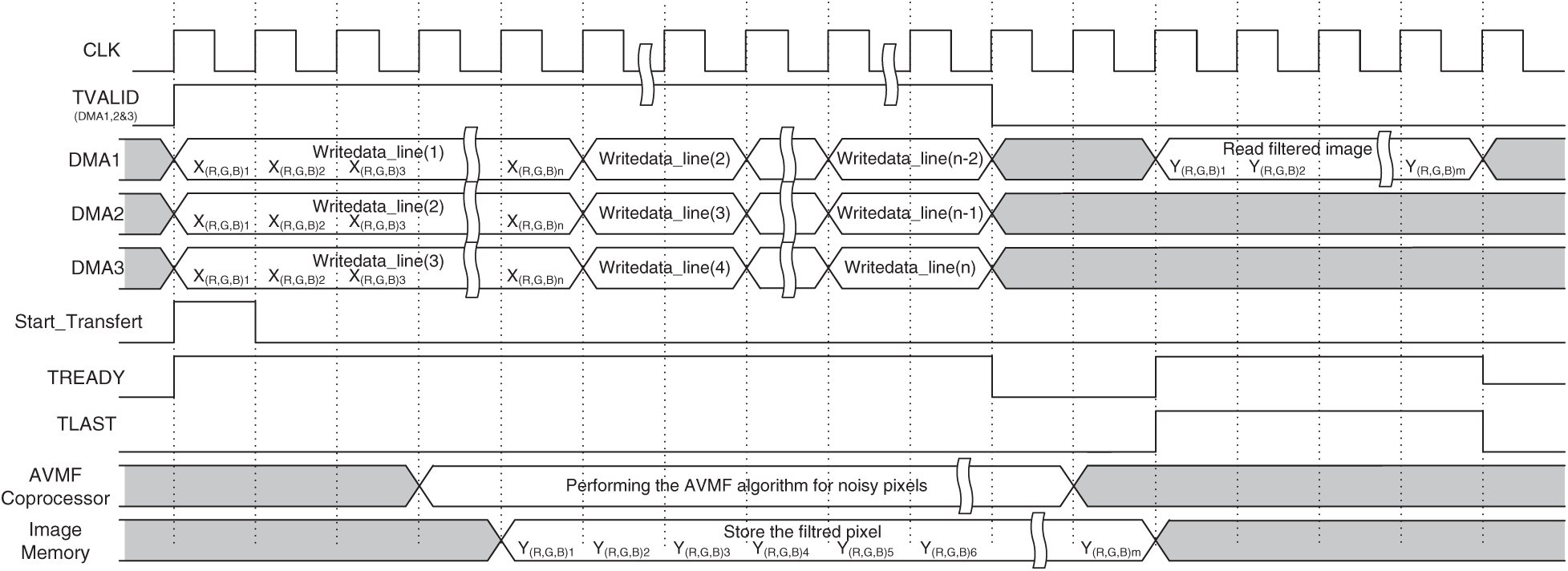
Figure 8: Behavior of the SW/HW AVMF design
To evaluate the proper functioning of the SW/HW AVMF design for the HLS ideal and optimized HW IPs blocks, we have followed the design flow which is presented in Fig. 9. In fact, the Vivado HLS is used to apply directives and create a stream interface in order to connect the IP blocks with the processor. After that, when the HLS synthesis is completed, the compressed file (.ZIP) including all HDL files is generated and exported to the Xilinx Vivado tool which is used to implement a multiple accelerators blocks connected to the embedded processor across an AXI interface. Then, the Xilinx Vivado tool is used to synthesis, implement the SW/HW design and generate and load the Bitstream file (.bit) in the FPGA platform. Besides, the SW is carried out using the ARM Cortex-A9 processor and compiled with a standalone application using the Xilinx software development toolkit (SDK) to generate the executable file (.elf) which will be performed per the embedded processor.
Tab. 4 reports the implementation results for the ideal and optimized SW/HW AVMF design under the XC7Z020 FPGA. It is obvious from this table that the optimized SW/HW AVMF design presents a decrease per nearly 45% in the number of LUTs and 22% in the number of DSPs compared to the ideal SW/HW design.
The next step consists in evaluating the performance in terms of the processing time, power consumption and image quality parameters under the ZC702 FPGA board. The processing time measurement is done by means of the processor timer while power consumption is measured by the Texas Instruments fusion digital power designer software using the Texas Instruments device which is connected to the ZC702 board through a USB interface adapter. Accordingly, taking subjective measurement as an effective way of judging the efficiency of the filter, from Fig. 10, we can see that the implemented filter conserves the chromaticity components as well as the fine details of a color image (Monalisa) using 3% of impulsive noise. Consequently, no differences are noticeable between the images filtered by the SW/HW solutions and those in the output of the SW solutions (ideal and optimized).
To prove that, the NCD and the Peak Signal to Noise Ratio (PSNR) are used in these simulations and performed for different standard test images (Lena, Flower, Peppers, Sailboat, Mandrill, Monalisa). The size of these color images is 256

Figure 9: HLS flow of the SW/HW AVMF design
Table 4: SW/HW implementation results


Figure 10: (1) Original RGB images, (2) noisy RGB images, filtered RGB images with (3) ideal SW, (4) ideal SW/HW, (5) optimized SW, and (6) optimized SW/HW
Table 5: Comparisons of the PSNR values for the SW/HW and the SW AVMF designs

Compared to other realizations, we can notice from Tab. 8 that our design produces better performance results than in [8] for the floating-point implementation of the AVMF filter. As a matter of fact, the throughput of our design is 6.8 times faster than [8]. Moreover, our design has better performance than results in [29,30] which present the floating-point implementation of AVMF and VMF filters in Intel Core (TM) i7-4790 at 3.2 GHz and DSP TMS320C6701 at 150 MHz, respectively. It is crucial to mention that our design is implemented on the ZC702 board which has an ARM cortex-A9 core running on 667 MHz and the IP was implemented with a 100 MHz clock frequency. On the other hand, the throughput of our design is 4.9 times faster than [27] for the fixed-point implementation of the AVMF filter in SW/HW environment. Knowing that, it is important to remind that the LLS method is used in [27].
Table 6: Comparisons of NCD values for the SW/HW and the SW AVMF designs

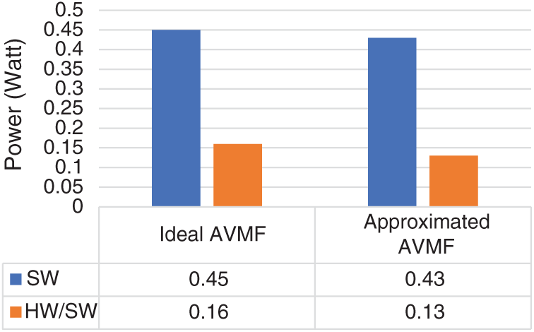
Figure 11: Power consumption measurement for the SW/HW and SW AVMF designs
Table 7: Comparisons of processing time for the SW/HW and SW AVMF designs

In light of the above findings, the HLS approach presents a good solution to elevate the abstraction level from RTL to algorithms and accelerate both the design time and the time to market (TTM). But, we can notice that with HLS approach, the reference software should be rewrite in a specific format and select the right directives to attain a better performance in terms of FPGA area cost, power consumption and processing time. Thus, for example with the Xilinx Vivado HLS, the ALLOCATION directive allows to reduce the FPGA area cost. Moreover, the PIPELINE and ARRAY PARTITION directives can be used to improve pipeline and parallel processing between loop iterations which helps to reach higher throughput. Besides, it becomes possible to design a HW floating-point architecture where the performance in terms of processing time and power consumption is better than that of the SW solution and with the same QoR. Further, HLS approach can be combined with SW/HW design methodology to guarantee on the one hand the acceleration of the conception and the flexibility to update the design, on the other hand the performance in terms of processing time and power consumption.
Table 8: Performance comparisons of the filter implementation

In this work, the HLS approach is used to design floating-point and fixed-point hardware architectures for the AVMF filter by applying specific directives (ALLOCATION, PIPELINE and ARRAY PARTITION) to the AVMF C codes. The first design was based on the square root function (ideal HW). The second design was based the ROM memory (optimized HW). These designs are integrated as coprocessor with ARM cortex-A9 processor in the SW/HW environment. The AXI-stream interface is used to speed up the data transfer between the PL part and the DDR memory. The experimental results under the ZC702 FPGA platform show that the SW/HW AVMF designs give a better performance in terms of processing time, power consumption and hardware cost relative to the SW implementation with the same QoR. These results prove not only the efficiency of HLS tool, but also the reliability of the proposed SW/HW AVMF design which can be used for several image sizes.
Acknowledgement: The authors would like to express their deepest gratitude to Prof. Ali M. AMRI of ENET’Com, University of Sfax, Tunisia, for his meticulous proofreading of their paper.
Funding Statement: The authors extend their appreciation to the Deanship of Scientific Research at Jouf University (Kingdom of Saudi Arabia) for funding this work through research Grant No. DSR2020-06-3663.
Conflicts of Interest: The authors declare that they have no conflicts of interest to report regarding the present study.
1. S. Wang and C. Wu, “A New impulse detection and filtering method for removal of wide range impulse noises,” Pattern Recognition, vol. 42, no. 9, pp. 2194–2202, 2009. [Google Scholar]
2. Z. Ramadan, “Monochromatic-based method for impulse noise detection and suppression in color images,” Circuits, Systems, and Signal Processing, vol. 32, no. 4, pp. 1859–1874, 2013. [Google Scholar]
3. H. Jagadish and J. Prakash, “A new approach for denoising remotely sensed images using DWT based homomorphic filtering techniques,” International Journal of Emerging Trends & Technology in Computer Science, vol. 3, no. 3, pp. 90–96, 2014. [Google Scholar]
4. Q. Wang, W. Shi, Z. Li and P. Atkinson, “Fusion of sentinel-2 images,” International Archives of the Photogrammetry, Remote Sensing of Environment, vol. 187, pp. 241–252, 2016. [Google Scholar]
5. I. Pitas and A. Vanetsanpoulas, “Nonlinear mean filters in image processing,” IEEE Transaction on Acoustics, Speech, Signal Processing, vol. 34, no. 3, pp. 573–584, 1986. [Google Scholar]
6. R. Shapley, “Linear and nonlinear systems analysis of the visual system: Why does it seem so linear?: A review dedicated to the memory of Henk Spekreijse,” Vision Research, vol. 49, no. 9, pp. 907–921, 2009. [Google Scholar]
7. J. Astola, P. Haavisto and Y. Neuvo, “Vector median filter,” Proceedings IEEE, vol. 78, no. 4, pp. 678–689, 1990. [Google Scholar]
8. L. Rastislav, P. N. Konstantinos, V. N. Anastasios and S. Bogdan, “A statistically-switched adaptive vector median filter,” Journal of Intelligent and Robotic Systems, vol. 42, no. 4, pp. 361–391, 2005. [Google Scholar]
9. L. Khriji and M. Gabbouj, “Vector median-rational hybrid filters for multichannel image processing,” IEEE Signal Processing Letters, vol. 6, no. 7, pp. 186–190, 1999. [Google Scholar]
10. A. Boudabous, L. Khriji, A. Ben Atitallah, P. Kadionik and N. Masmoudi, “Efficient architecture and implementation of vector median filter in co-design context,” Radioengineering-Prague, vol. 16, no. 3, pp. 113–119, 2007. [Google Scholar]
11. A. Boudabous, A. Ben Atitallah, L. Khriji, P. Kadionik and N. Masmoudi, “Hardware implementation and experiment validation of the VDDRHF color image filter,” in 7th Int. Multi-Conf. on Systems, Signals and Devices, Amman, Jordan, 2010. [Google Scholar]
12. B. Trivedi, J. Popat and K. Govani, “Optimized implementation of median filter algorithm on FPGA,” International Journal of Emerging Technologies and Applications in Engineering, Technology and Sciences, vol. 7, no. 1, pp. 246–249, 2014. [Google Scholar]
13. Y. Hu and H. Ji, “Research on image median filtering algorithm and its FPGA implementation,” in WRI Global Congress on Intelligent Systems, Xiamen, China, pp. 226–230, 2009. [Google Scholar]
14. M. A. Vega-Rodríguez, J. M. Sánchez-Pérez and J. A. Gómez-Pulido, “An FPGA-based implementation for median filter meeting the real-time requirements of automated visual inspection systems,” in 10th Mediterranean Conf. on Control and Automation, Lisbon, Portuga, 2002. [Google Scholar]
15. T. W. Lee, J. H. Lee and S. B. Cho, “FPGA implementation of a 3/SPL times/3 window median filter based on a new efficient bit-serial sorting algorithm,” in The 7th Korea–Russia IEEE Int. Symp. on Science and Technology, Ulsan, South Korea, pp. 237–242, 2003. [Google Scholar]
16. A. Boudabous, A. Ben Atitallah, L. Khriji, P. Kadionik and N. Masmoudi, “HW/SW design-based implementation of vector median rational hybrid filter,” International Arab Journal of Information Technology, vol. 7, no. 1, pp. 70–74, 2010. [Google Scholar]
17. M. Kthiri, B. Le Gal, P. Kadionik and A. Ben Atitallah, “A very high throughput deblocking filter for H.264/AVC,” Journal of Signal Processing Systems, vol. 73, no. 2, pp. 189–199, 2013. [Google Scholar]
18. A. Ben Atitallah, P. Kadionik, F. Ghozzi, P. Nouel, N. Masmoudi et al., “Optimization and implementation on FPGA of the DCT/IDCT algorithm,” in IEEE Int. Conf. on Acoustics Speech and Signal Processing Proc., Toulouse, France, 2006. [Google Scholar]
19. A. Ben Atitallah, M. Kammoun, K. M. A. Ali and R. Ben Atitallah, “An FPGA comparative study of high-level and low-level combined designs for HEVC intra, inverse quantization, and IDCT/IDST 2D modules,” International Journal of Circuit Theory and Applications, vol. 48, no. 8, pp. 1274–1290, 2020. [Google Scholar]
20. M. Kammoun, A. Ben Atitallah, K. M. Ali and R. Ben Atitallah, “Case study of an HEVC decoder application using high-level synthesis: Intra prediction, dequantization, and inverse transform blocks,” Journal of Electronic Imaging, vol. 28, no. 3, pp. 1, 2019. [Google Scholar]
21. Intel, “OpenCL Intel Corporation,” 2019. [Online]. Available: https://www.intel.com/content/www/us/en/tool/programmable/sdk-for-opencl/overview.html. [Google Scholar]
22. CALYPTO, “Catapult C Synthesis,” 2021. [Online]. Available: https://eda.sw.siemens.com/en-US/ic/catapult-high-level-synthesis/. [Google Scholar]
23. J. Villarreal, A. Park, W. Najjar and R. Halstead, “Designing modular hardware accelerators in C with ROCCC 2.0,” in 18th IEEE Annual Int. Symp. on Field-Programmable Custom Computing Machines, Charlotte, NC, USA, 2010. [Google Scholar]
24. R. Nane, V. M. Sima, C. Pilato, J. Choi, B. Fort et al., “A survey and evaluation of FPGA high-level synthesis tools,” IEEE Transactions on Computer-Aided Design of Integrated Circuits and Systems, vol. 35, no. 10, pp. 1591–1604, 2016. [Google Scholar]
25. A. Ben Atitallah, H. Loukil, P. Kadionik and N. Masmoudi, “Advanced design of TQ/IQT component for H.264/AVC based on SoPC validation,” WSEAS Transactions on Circuits and Systems, vol. 11, no. 7, pp. 211–223, 2012. [Google Scholar]
26. M. Kammoun, A. Ben Atitallah, R. Ben Atitallah and N. Masmoudi, “Design exploration of efficient implementation on SOC heterogeneous platform: HEVC intra prediction application,” International Journal of Circuit Theory and Applications, vol. 45, no. 12, pp. 2243–2259, 2017. [Google Scholar]
27. I. Abid and A. Ben Atitallah, “An optimized sequential architecture of the AVMF filter,” in 4th Int. Conf. on Recent Advances in Electrical Systems, Hammamet, Tunisia, pp. 48–52, 2019. [Google Scholar]
28. Xilinx, “Xilinx Zynq-7000 SoC ZC702 Evaluation Kit,” 2021. [Online]. Available: https://www.xilinx.com/products/boards-and-kits/ek-z7-zc702-g.html. [Google Scholar]
29. L. Jin, Z. Zhu, E. Song and X. Xu, “An effective vector filter for impulse noise reduction based on adaptive quaternion color distance mechanism,” Signal Processing, vol. 155, no. 12, pp. 334–345, 2019. [Google Scholar]
30. L. C. Dominguez and V. I. Ponomaryov, “Non-Linear filters for colour imaging implemented by DSP,” in 2nd Int. Conf. on Electrical and Electronics Engineering and XI Conf. on Electrical Engineering, Mexico City, Mexico, 2005. [Google Scholar]
 | This work is licensed under a Creative Commons Attribution 4.0 International License, which permits unrestricted use, distribution, and reproduction in any medium, provided the original work is properly cited. |