DOI:10.32604/cmc.2021.018292
| Computers, Materials & Continua DOI:10.32604/cmc.2021.018292 | |
| Article |
Design of a Five-Band Dual-Port Rectenna for RF Energy Harvesting
1Centre for Wireless Technology, Faculty of Engineering, Multimedia University, Cyberjaya, 63100, Malaysia
2College of Computer Science and Engineering, Prince Sattam Bin Abdulaziz University, Alkharj, 11942, Saudi Arabia
*Corresponding Author: Surajo Muhammad. Email: doguwa_2002@yahoo.com
Received: 02 March 2021; Accepted: 04 April 2021
Abstract: This paper proposed the design of a dual-port rectifier with multi-frequency operations. The RF rectifier is achieved using a combination of L-section inductive impedance matching network (IMN) at Port-1 with a multiple stubs impedance transformer at Port-2. The fabricated prototype can harvest RF signal from GSM/900, GSM/1800, UMTS/2100, Wi-Fi/2.45 and LTE/2600 frequency bands at (0.94, 1.80, 2.10, 2.46, and 2.63 GHz), respectively. The rectifier occupies a small portion of a PCB board at 0.20 λg × 0.15 λg. The proposed circuit realized a measured peak RF-to-dc (radio frequency direct current) power conversion efficiency (PCE) of (21%, 22.76%, 25.33%, 21.57%, and 22.14%) for an input power of −20 dBm. The RF harvester attains a measured peak RF-to-dc PCE of 72.70% and an output dc voltage of 154 mV for an input power of 3 dBm at 2.46 GHz. Measurement of the proposed rectifier in the ambiance gives a peak dc output voltage of 376.1 mV from the five signal tones. Similarly, a low-powered bq25504-674 evaluation module (EVM) is integrated with the rectifier. The module boost and drive the rectifier output dc voltage to 945 mV. The performance of the proposed rectifier in the ambiance environment makes it a suitable module for low-powered RF applications.
Keywords: RF energy harvesting; impedance matching network; power conversion efficiency; multi-band rectifier
The evolution and advancement of wireless communications technology contribute immensely to the exponential growth of wireless devices in our day-to-day activities [1]. The emergence of technologies for low-powered applications in the field of security surveillance, health care systems, agriculture, along with other vital application drivers, attracted the attention of researchers in the area of wireless power transfer (WPT) and RFEH [1–3]. A reliable energy source is one of the key challenges with the growing ultra-low-powered devices [4]. To overcome the challenges of battery-based conventional devices. RFEH technology is considered to provide direct power and battery recharging from the electromagnetic (EM) energy [4]. In order to address the limitation of the conventional battery-based devices of charging, maintaining, or replacing a battery. The propagation of EM wave in space that carries an EM radiant energy from various sources makes it applicable as an additional source of energy for low-powered devices [3]. The RFEH circuit is accomplished through a rectifying antenna (rectenna) comprising a receiving antenna, an IMN, a rectifying diode, a dc-pass filter, and a terminal load [5].
The RFEH antenna picks relatively low AC signals. Hence, a conditioning circuit for maximum transfer of power between the antenna and the rectifying diode to the load terminal is of paramount importance [2,5]. The RF rectifier is a vital component of the RFEH circuit that matches and converts the received AC signal from the antenna to the equivalent dc output through an IMN, a rectifying diode, a dc-pass filter, the load terminal. Rectenna operates at a designated frequency with a significant RF power density to ensure a reliable operation of the circuit [1,6].
Various researchers have reported works on RFEH circuits for single-band [7,8], dual-band [9], and multi-band [1,6–10], operations. The authors in [6] present a quad-band (1.3, 1.7, 2.4, 3.6 GHz) rectifier using a distributed T-section IMN. The authors in [11] reported a triple-band (0.94, 1.95, and 2.44 GHz) RF rectifier control by a 4-stage single dual-diode matched through a single L-section IMN. A four-band (0.95, 1.83, 2.45, and 2.62 GHz) RF harvester using two-branches of 4-stage voltage multiplier is reported by the authors in [12]. The RFEH harvester in [6,11], and [12] are suitable for high-power applications because of the complexity of the circuits that increase the parasitic capacitance across the junction of the diode. In [13], the authors reported a triple-band (2, 2.5, and 3.5 GHz) rectenna. The authors in [14] present a four-band (0.89, 1.27, 2.02, and 2.38 GHz) rectifier comprising a series diode D1 and a combination of shunt field-effect transistor (FET) with a second diode D2. The Circuit in [14] is matched through a cross-shaped stub and a stepped impedance microstrip line. The rectifier operating frequency by the authors in [6] at 3.6 GHz, [13] at (2 and 3.5 GHz), and [14] at (1.27 and 2.02 GHz) contributes little RF power density to the RF harvester. The authors in [10] reported a multi-port rectenna with the ability to explore spatial domain through multiple receiving antennas. A single band (98 MHz) low-frequency frequency modulated (FM) RF harvester is slotted into a triple-band (0.88, 1.7, and 2.370 GHz) four-cornered multi-port rectenna. The narrow bandwidth associated with the design does not sufficiently exploit the frequency domain of the EM spectrum, besides the two-level dc-combiner that introduces additional losses into the transmission line. It is worth mentioning that most of the rectenna and RF rectifiers reported from the literature have limited operational bandwidth between (20–40 MHz). Besides operating at a high input power, some works presented have insignificant RF power density to harvest and manage by the rectifier.
In this paper, a compact dual-port rectenna with the ability to cover most of the EM spectrum with a significant RF power density is proposed. The proposed rectifier operates at (0.94, 1.80, 2.10, 2.46, and 2.63 GHz) matched through a 2.5 kΩ load terminal. The proposed rectenna harvests RF signals from GSM/900, GSM/1800, UMTS/2100, Wi-Fi/2.45, and LTE/2600 frequency bands. Improvements in compactness, operational bandwidth, and the overall RF-to-dc PCE were seen in the proposed design. The design is a promising candidate for many applications in low-powered systems. In this paper, the design of the rectifier circuit is discussed in Section 2, and Section 3 presents the performance of a dual-port rectifier. Section 4 highlights the design of a wideband antenna to complete a rectenna. The rectenna measurement results in the ambiance environment are reported in Section 5, and Section 6 concludes the work.
An RFEH system requires a rectifying diode to handle a low input power at high frequency with minimum losses [7,5]. A single diode RF rectifier configuration shows a better performance at low input power than its equivalents single or multi-stage voltage multiplier [2]. Hence, a single-series diode circuit topology is considered here in this work to minimize junction parasitic and ensure a faster switching time [4,15]. Fig. 1 presents a typical single-series RF rectifier topology using a shunt capacitor filter. To minimize the passage of higher-order harmonics into the load, a shunt dc-pass filter is added between the diode and the load terminal (RL).
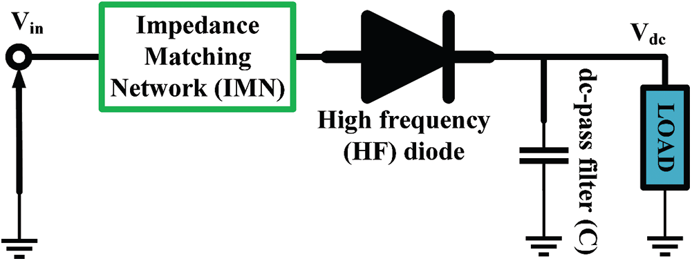
Figure 1: A Conventional single series RF rectifier topology
Fig. 2 presents the model layout of the proposed dual-port wideband rectifier. Two IMN design approach is adopted at each port to reduce circuit complexity and ensure a compact harvester. The first section of the proposed rectifier (Rectifier1) is designed at 0.93 GHz using a second-order L-section matching network (MN) for harvesting GSM/900 available power. Rectifier-1 is connected through Port-1. Port-2 is used to connect the second segment of the rectifier (Rectifier-2), comprising three cell branches matched through an impedance transformer network. Each cell branch is matched to a single series diode D2–D4 at 1.8, 2.1, and 2.45 GHz, respectively.
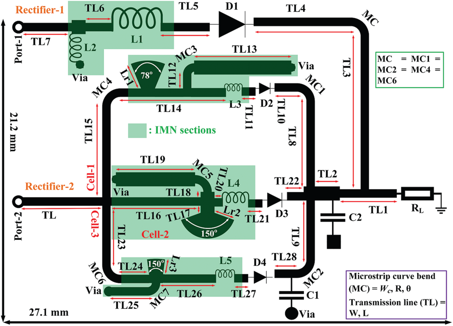
Figure 2: Proposed EM model layout of the rectifier. The parameters are optimized as: L = 5.8, L1 = 2.6, L2 = L10 = L28 = Lr2 = 1.6, L3 = L4 = 11, L5 = 9, L6 = 2, L7 = 3.5, L8 = 6.1, L9 = L23 = 4.25, R = L11 = L12 = L21 = L27 = 1, L13 = 7, L14 = 9, L15 = 6.5, L16 = 9, R7 = L17 = L18 = L20 = 0.6, L19 = 5.7, L22 = 1.2, L24 = 5, L25 = 2.8, L26 = 3, W = W1 = W3 = W4 = W5 = W6 = W7 = W8 = W9 = W10 = W11 = W12 = W14 = W15 = W16 = W20 = W22 = W23 = W24 = W25 = W26 = W27 = W28 = 0.6, W2 = W13 = W17 = W18 = W19 = W21 = 1, Wc = Wc3 = Wc5 = Wc7 = 0.6, R3 = 0.5, R5 = 0.9, Lr1 = 1.9, Lr3 = 1.1: (All units are in mm). θ = θ1 = θ2 = θ3 = θ4 = θ5 = θ6 = θ7 = 90°, L1 = 22 nH, L = 6.2 nH, C1 = C2 = 200 pF, L3 = 10 nH, L4 = 8.2 nH, L5 = 4.7 nH, 2.5 kΩ
The rectifier sections are designed on a high-frequency single-series HSMS-2850 low-powered Schottky barrier diode from Avago. The diode exhibit a small junction capacitance of 0.18 pF, a forward biasing voltage of 150 mV. SOT-323 provides the diode physical configuration layout [1,5]. The proposed rectifier is designed and constructed on a 1.6 mm thick FR-4 substrate (with a dielectric constant of 5.4 and a loss tangent of 0.02). The dual-port RF rectifier is terminated with a 50 Ω source through a transmission line at Port-1 and Port-2.
The input impedance of Rectifiers-1 and 2 are first computed without an MN comprising only a rectifying diode, dc-pass capacitor filter, and a load terminal. The dc-pass capacitor filter is designed to smoothing the peaks from the output of the rectifying diode and also reject higher-order harmonics [16]. A source pool simulation using a harmonic balance (HB) solver is executed to determine a suitable value of RL in advance design system (ADS). A 200 pF capacitor filter shunt with a 2.5 kΩ load terminal offers a better trade-off performance across the proposed rectifier operating frequencies.
The input impedance of Rectifier-1 is matched to the 50 Ω transmission line through an L-section MN comprising two inductors L1, and L2. The evaluation of the MN parameters at a specified frequency is accomplished by canceling the imaginary reactance of a source and load and then compare their equivalent real part. Eqs. (1)–(6) provides the model equations of the MN.
By comparing the real part of the antenna with the rectifier input impedance Zin, we get:
where Rant = source impedance of the antenna at 50 Ω, Rin = rectifier input impedance. The quality factor Q is given by:
The inductance L2 can be determined from the definition of a quality factor as:
where Cin = reactive components of the load impedance operating at angular frequency ωo. From Eq. (3), L1 is given by:
The value of L2 can be determined through parallel to series transformation. We then equate the resultant imaginary part to zero, as:
L2 can be express from Eq. (5), as:
The elements of the MN (L1 and L2) were first determined at (68 and 0.1 nH) using a 50 Ω transmission line at 0.93 GHz. An ideal components palette in ADS was used to transfer the equivalent parameters into the design. The parameters are then tuned to balance the effects of the transmission line at (36 and 3.78 nH), respectively. Ideal inductor elements were substituted with the equivalent S-parameter files from muRata in the ADS library to ensure the optimization of Rectifier-1 as close as possible. The parameters of the MN were further tuned and optimized at (22 and 6.2 nH) with part number of LQG18HN22NJ00D and 0603 circuit layout, respectively.
RF rectifier with a wide impedance bandwidth is vital in achieving a reliable RFEH module [16]. Normally, the input impedance of the rectifying diode in the MN design depends on the operating frequency with a narrow bandwidth [16]. The method of combining RF rectifiers operating at a single or dual band in parallel for a wide bandwidth is reported in [2,8,10–17]. The technique ensures maximum transfer of the harvested power through the load terminal with a meaningful signal contribution across each signal tone. The concept is adopted in the second section of the proposed rectifier (Rectifier-2). It is composed of three (3) cell blocks cascaded in parallel as (Cell-1–Cell-3) by Port-2. A curve shunt stub impedance transformer was first designed to match a single band rectifier with a 50 Ω transmission line at 1.8, 2.1, and 2.40 GHz, respectively.
The resonant length of each shunt stub is calculated at λ/8 of the guided wavelength at the three operating frequencies, respectively. The length of the stub is first computed at (9, 8.5, and 7.2 mm) for the three respective cell blocks. The parameters are then transferred into the ADS by integrating a microstrip curve bend (MCURVE) with a microstrip line (MLINE) to the diode for each cell. Length of each shunt transformer is tuned to match the input impedance of the 50 Ω transmission line to the conjugate of the rectifying diode through the load. To minimize the length and losses of the transmission line, an inductor elements from muRata is added into the MN of each cell. Connecting the inductor to the anode terminal of the diode also improves the input signal going into the rectifying diode. To improve the bandwidth of the rectifier at each operating frequency, a shunt radial stub is loaded into the MN of each cell. The use of the inductor and the radial stub helps ensure the rectifier compactness with an additional degree of freedom. The three cells of Rectifier-2 are integrated through transmission lines (TL6, TL7, TL12, and TL19) to maintain a practical design. Cascading the three cell block creates further parametric tuning to achieve the desired result. Cells-1 and 2 are linked through a dc-pass filter (C2) and the load terminal (RL). The two cells are tuned and optimized through 10 and 8.2 nH inductors from muRata (with LQG18HN10NJ00D part number and 0603 circuit layout) for 1.8 and 2.1 GHz operating frequency, respectively. Cell-3 design covers a broader operating bandwidth (2.33–2.67 GHz), the cell is optimized with a 4.7 nH inductor (having a part number of LQG15HS4N7S02D 0402 circuit layout). The cathode terminal of the diode D4 is shunt with a capacitor C1 to minimize interference between the three cells. To provide dc biasing into the rectifier circuit, curve shunt transformers and capacitors are shorted to the ground through Vias. C1 and C2 are having a part number of GRM1885C1H201JA01 and 0402 circuit layout.
The source connecting Port-2 is modeled as a 50 Ω power source with four signal tone at 1.80, 2.10, 2.41, and 2.60 GHz in ADS. The equivalent AC source at Port-1 and Port-2 is guided by a wave Eq. (7).
where VS is the input voltage from the source, and VSMAX represents maximum amplitude RF input signal entering the rectifying diode at an angular frequency ω.
A dc combiner is used to connect the resulting output dc signal from the two rectifiers through a load terminal RL. The whole proposed circuit is realized from a set of two (2) capacitors, five (5) inductors, four (4) rectifying diodes, and a single load terminal RL.
The overall rectifier was fine-tuned and optimized. Carrying out this process lowers down additional parasitic in the design and compensate for the losses from a transmission line interconnection, components tolerance of the chip, soldering lead, and SMA source in the circuit. The optimized parameters of the proposed design are presented in Fig. 2.
The proposed dual-port rectifier is designed and fabricated on a double layer FR-4 substrate using a full ground architecture as presented in Fig. 3a. The rectifier is then connected with a pair of crocodile clips across the load terminal for easy performance evaluation. A vector network analyzer (VNA) E5062A is deployed to measure the rectifier input reflection coefficient (S11). The measured and simulated S11 of the proposed rectifier is reported in Fig. 3b. The proposed designed achieved a simulated S11 towards a −10 dB reference point at 0.93 GHz (0.90–0.97 GHz) for Rectifier-1 and 1.8 GHz (1.760–1.850 GHz), 2.1 GHz (2.04–2.160 GHz), and 2.41 GHz/2.6 GHz (2.33–2.670 GHz) for Rectifier-2. The fabricated prototype shows a good agreement with the simulated results having, S11 at 0.94 GHz (0.91–0.98 GHz) for Rectifier-1 and 1.8 GHz (1.750–1.855 GHz), 2.1 GHz (2.03–2.170 GHz), and 2.46 GHz/2.63 GHz (2.37–2.70 GHz) for Rectifier-2. The results show the rectifier capability to harvest RF signal from GSM/900, GSM/1800, UMTS/2100, Wi-Fi/2.45, and LTE/2600 frequency bands. S12 is used to determine the isolation between Port-1 and Port-2. The measured values of S12 are (59.65, 25.18, 43.51, 49.90, and 52.42 dB) at (0.94, 1.8, 2.1, 2.46, and 2.63 GHz), respectively.
The measured and simulated RF-to-dc PCE of the proposed dual-port rectifier against frequency is presented in Fig. 4. Frequency sweeping across the 2.5 kΩ load is carried out between 0.8 to 2.8 GHz at four different input power levels (−30 to 0 dBm at an interval of 10 dBm). The measurement is performed separately at Port-1 and Port-2. The rectifier performance evaluation is achieved by using a HB simulator with a parameter sweep in ADS. The measurement of the RF-to-dc PCE against input power Pin is conducted by connecting the rectifier with a 12 GHz AnaPico signal generator (APSIN12G). A low power signal from the generator (varied between −30 to 5 dBm at an interval of 2 dBm) is supplied to the rectifier at each operating frequency. A digital multi-meter is used to record the output dc voltage separately for Port-1 and Port-2. The values are recorded across the 2 kΩ terminal load at each sampling point.
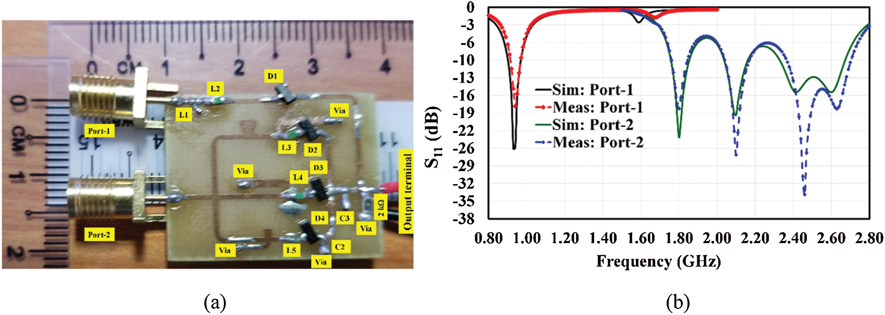
Figure 3: Proposed rectifier: (a) Fabricated prototype (b) Simulated and measured reflection coefficient S11 at Port-1 and Port-2
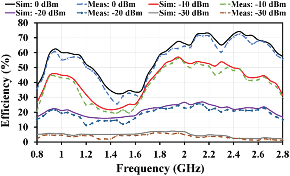
Figure 4: Simulated and measured RF-to-dc PCE against frequency at four different RF input power levels Pin for Port-1 and Port-2
From the dc output voltage results, the rectifier RF-to-dc PCE for Port-1 and Port-2 are computed using:
where ηPCE is the rectifier RF-to-dc PCE and Pdc is the equivalent dc output power across RL. Pin denotes the RF source signal at the input terminal of the rectifier. Vdc gives the equivalent output dc voltage across the load terminal RL.
The total RF-to-dc PCE for the dual-port rectifier is given by:
where ηmax represents the total RF-to-dc PCE from the two ports. Pin1 and Pin2 denote the RF signal that goes into the rectifier through Port-1 and Port-2. Vdc1 and Vdc2 provide the equivalent output dc voltage across the load RL.
The measured and simulated RF-to-dc PCE against the input signal (Pin) is presented in Figs. 5a and 5b. The proposed multi-band rectifier realized a measured maximum RF-to-dc PCE of 61.31% for an input power of 3 dBm at 0.94 GHz and 57.67%, 71.90%, 72.7%, and 70.0% for an input power of 0, −1, 0, and 1 dBm at (1.80, 2.10, 2.46, and 2.63 GHz), respectively. At a low input power, the proposed rectifier realized a measured peak RF-to-dc PCE of 21%, 22.76%, 25.33%, 21.57%, and 22.14% for an input power of −20 dBm, respectively. For the entire measuring process, when a single port is subjected to test, the other port is terminated with the 50 Ω impedance.
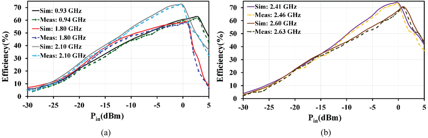
Figure 5: Simulated and measured RF-to-dc PCE of the proposed dual-port rectifier vs. Pin at (a) 0.94, 1.8, and 2.1 GHz (b) 2.46, 2.63 GHz
Fig. 6 shows the proposed rectifier measurement setups in the laboratory. S11 and the dc output voltage were measured individually at each port of the rectifier.
A plot of the proposed rectifier RF-to-dc PCE against the load RL is presented in Fig. 7 for an input power of 0 dBm. The rectifier realized maximum RF-to-dc PCE within the 2–3.5 kΩ load terminal range. A trade-off for the optimal operation of the rectifier is achieved at 2.5 kΩ.
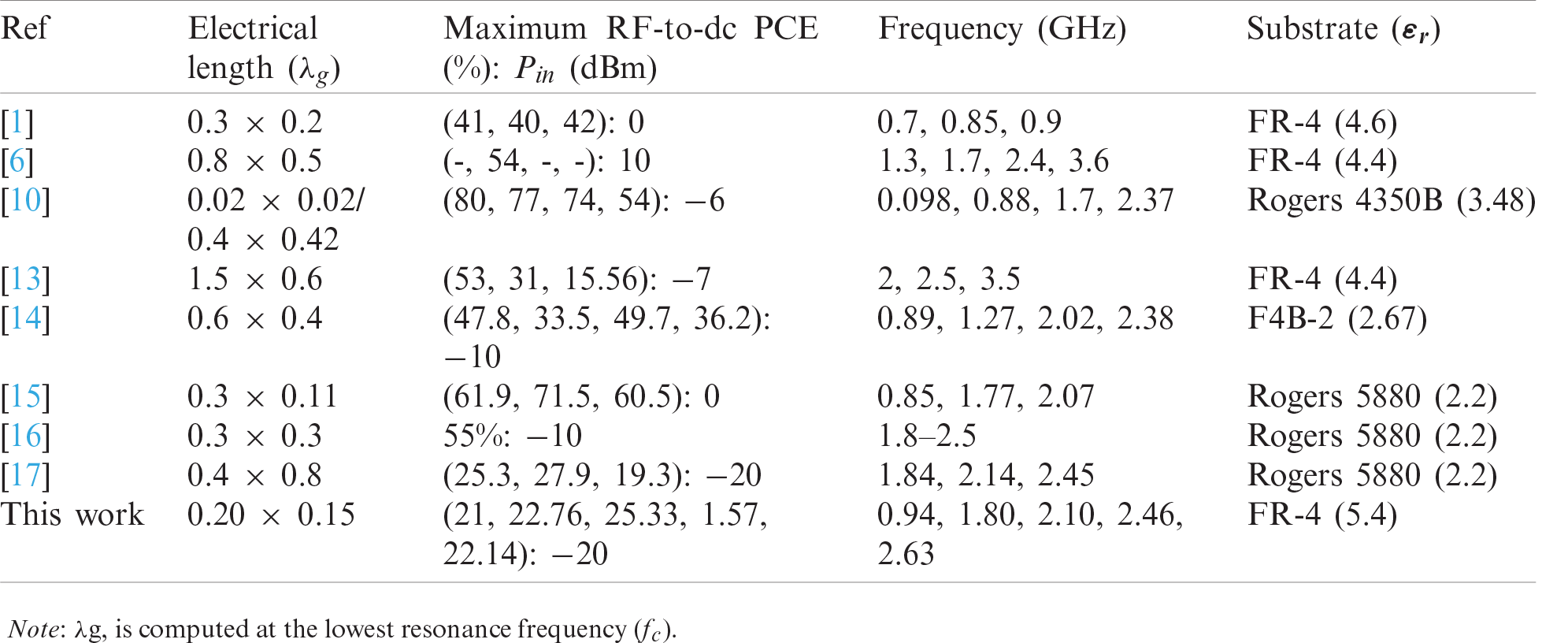
A comparison table between the proposed dual-port rectifier and previous related works from the literature is shown in Tab. 1. The manual setting of the MN reported by the authors in [1] makes the RF harvester impractical to be achieved. The rectifier reported by the authors in [15] has a narrow bandwidth across the designed frequencies as compares to our proposed work. The RF harvesters presented by the authors in [1] and [15] realized a peak RF-to-dc PCE for an input power of 0 dBm. The proposed dual-port RF harvester exhibit a better RF-to-dc PCE at 0 dBm of (59.57%, 57.70%, 71.0%, 72.7%, and 67.1%) across the five respective operating frequencies, in addition to a smaller electrical length. There is an insignificant RF signal to be harvested in some operating frequencies reported by the authors in [6] at 3.6 GHz and [14] at 1.27 GHz. The work in [6] is suitable for high power applications because it is optimized for an input of 10 dBm. It can be seen that the proposed dual-port RF harvester provides better RF-to-dc PCE and compactness as against the related designs presented in [6,13] and [14]. The first single band (98 MHz) rectifier presented in [10] operates at the direct line of sight (LOS) slotted in a triple-band RF harvester. The proposed design in this paper achieved a much smaller electrical length with a better operational bandwidth compared with related works in [10,17].
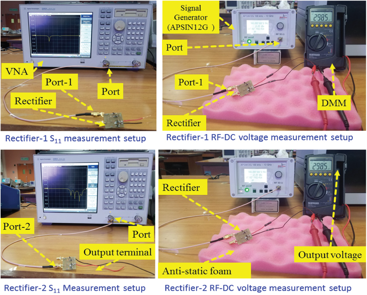
Figure 6: Proposed dual-port rectifier measurement setups at Port-1 and Port-2
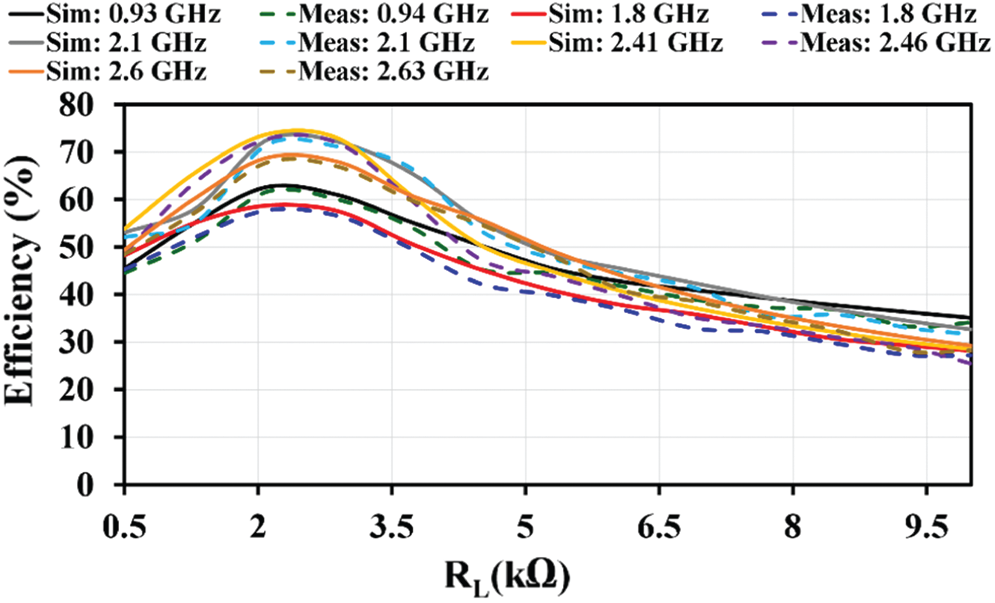
Figure 7: Proposed rectifier RF-to-dc PCE vs. terminal load RL at different operating frequencies for an input power of 0 dBm
Table 1: A comparison between the proposed dual-port rectifier and the previous related work
4 Wideband Receiving Antenna Design
The proposed wideband monopole antenna is designed from a rectangular patch of dimension 102 mm × 80 mm. The antenna is deployed because it offers wide bandwidth, ease of fabrication with a radiation pattern relatively close to the azimuthal omnidirectional pattern. Four triangular slots are first cuts through the rectangular radiating patch. A defected ground is deployed into the designed to achieve the desired bandwidth. A small rectangular slit is also added into the partial ground to improve the matching of the antenna. To achieve two resonance modes at 0.92 and 2.65 GHz, a semicircular slot of radius 11 mm and an arc of 32 mm diameter are added into the radiator, respectively. Two more equal semi equidistant circular slots of radius 4.1 mm are integrated to the lower arm of the rectangular patch to achieve more resonance mode in the upper bands 3.3 and 5.3 GHz, respectively. To improve the gain of the antenna in the lower band because of the partial ground effects. A circular parasitic patch of radius 13 mm is added to the ground plane. The antenna is fed through a 50 Ω source and is fabricated on the same FR-4 substrate. Because of its lightweight, low-cost, and ease of fabrication, the proposed RF rectifier and antenna are optimized on FR-4 substrate [5]. Fig. 8a provides the geometry of the proposed antenna with a total dimension of 140 mm × 90 mm × 1.6 mm.
The simulated and measured S11 of the proposed antenna is shown in Fig. 8b. The antenna achieved a simulated and measured bandwidth of (0.74 to 5.85 GHz) and (0.59 to 5.5 GHz), respectively. The antenna is a suitable candidate for GSM/900, GSM/1800, UMTS/2100, Wi-Fi/2.45, LTE/2600, WiMAX/3.5, and Wi-Fi/5GHz applications. The antenna attained a maximum measured gain of 4.12 dBi at 3.2 GHz. Fig. 9 presents the simulated and measured gain of the proposed wideband antenna with the fabricated prototype. The measured realized gain of the antenna at (0.92, 1.8, 2.1, 2.45, and 2.6 GHz) are (1.56, 3.05, 3.21, 4.15, and 4.68 dBi), respectively.
Fig. 10 provides the measured and simulated radiation pattern of the wideband monopole antenna along xz-plane having (ϕ = 0° | 0° < θ < 180°) and yz-plane for (ϕ = 90° | 0° < θ < 180°), respectively. The radiation pattern is measured and recorded at 0.92, 1.8, 2.1, 2.45, and 2.6 GHz operating frequencies. The results along xz-plane are close to that of a dipole antenna, and the yz-plane shows the attributes of a directional antenna.
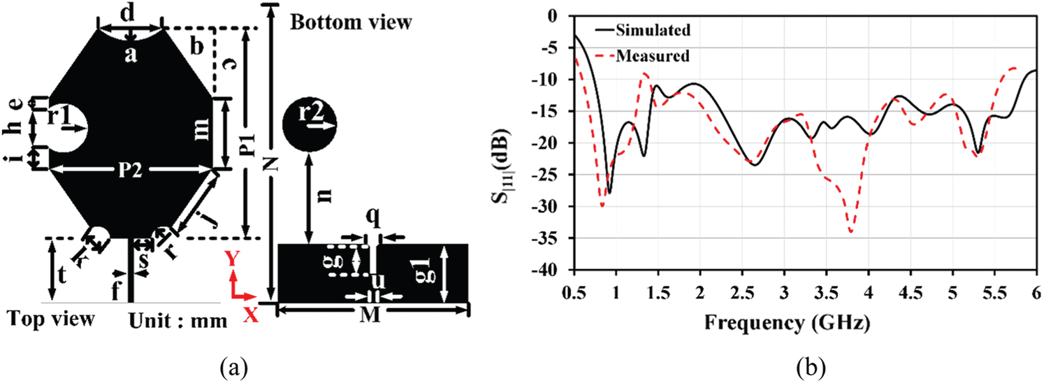
Figure 8: Proposed antenna (a) Geometry (b) Simulated and measured reflection coefficient S11 against frequency. The parameters are optimized as: M = 140, N = 90, P1 = 102, P2 = 80, a = 5.3, b = 24, c = m = 34, d = 32, e = 5, f = 2.8, g = 12.8, g1 = 28, h = 19, i = 10, j = 35.61, k = 10.65, n = 43, u = 3, q = 3.64, r = 4.1, r1 = 11.2, r2 = 13, s = 8.78, t = 31
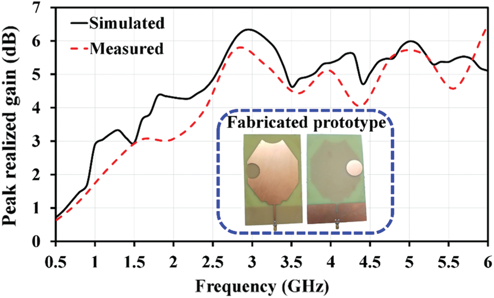
Figure 9: Simulated and measured realized gain of the proposed antenna
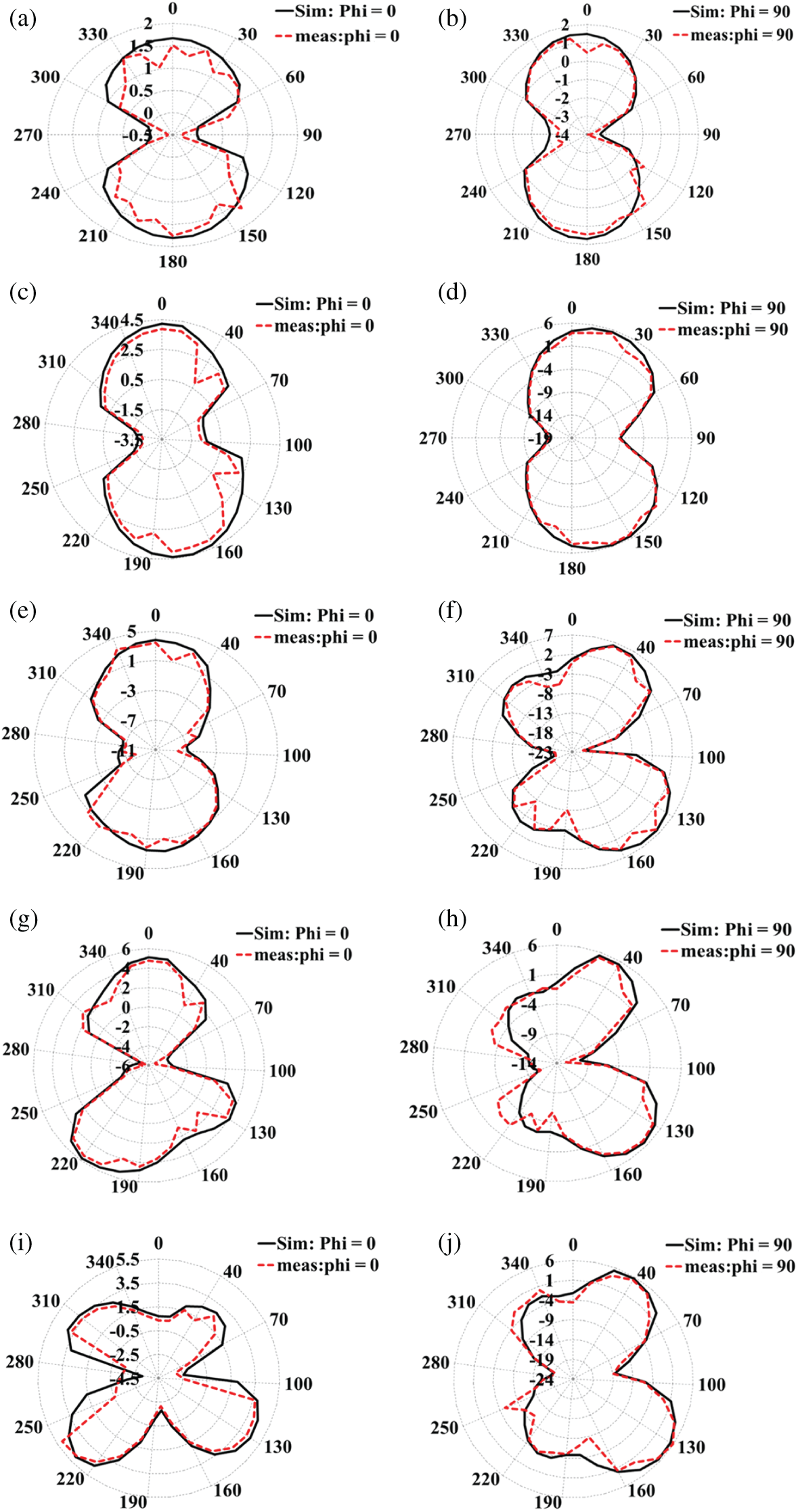
Figure 10: Simulated and measured radiation pattern of the proposed wideband monopole antenna for Phi = 0° and Phi = 90°: (a) and (b) at 0.92 GHz, (c) and (d) at 1.8 GHz, (e) and (f) at 2.1 GHz, (g) and (h) at 2.45 GHz, (i) and (j) at 2.6 GHz, respectively
5 Ambiance Measurement of the Proposed Rectenna
The proposed rectenna is tested in the ambiance environment. The measurement is carried out within Multimedia University, Cyberjaya Campus. The testing site is about 180 m apart from the nearby base station (BS) cell tower placed at 1mm high above the ground level. An ambient measurement setup is achieved using a pair of the fabricated antenna prototype. A 6 GHz (TTi PSA6005) spectrum analyzer (from Aim) is deployed to measure and record the available RF power density. The RF power densities across the five major frequency bands (GSM/900, GSM/1800, UMTS/2100, Wi-Fi/2.45, and LTE/2600) varies between (−37–−18 dBm, −35–−15 dBm, −45–−20 dBm, −50–−20 dBm, and −45–−20 dBm), respectively. Fig. 10 presents ambiance measurement of the proposed dual-port RF harvester. The two wideband antennae connect to the rectifier at Port-1 and Port-2. The proposed dual-port rectenna achieved a maximum output dc voltage of 376.1 mV from the available ambient RF power densities.
The RF input signal from the receiving antenna is a multitoned signal from multiple RF sources at the different operating frequencies. These signals vary with time and distance. Similarly, the rectifier output signals is a time-varying signal that needs to be stabilized through a power management module (PMM). The PMM is normally incorporated with storage elements such as micro-batteries and supercapacitor to manage the operations of low-powered devices [4,18]. In this paper, a low PMM (bq65504-674 EVM) from Texas Instruments is applied. A maximum power point tracking (MPPT) algorithm manages and samples the effective dc output voltage supply to the load or a storage element. This is achieved through a dc-dc converter integrated into the module, with the ability to enhance the output dc voltage to about 3.1 V. The module has a low startup input voltage of 130 and 330 mV, for a cold-start and hot-start, respectively, at a minimum quiescent current of 330 nA. Fig. 11 presents the setup of the proposed rectifier using bq25504-674 EVM. The proposed rectifier realized a maximum dc output voltage of 945 mV from the available ambient RF power densities.
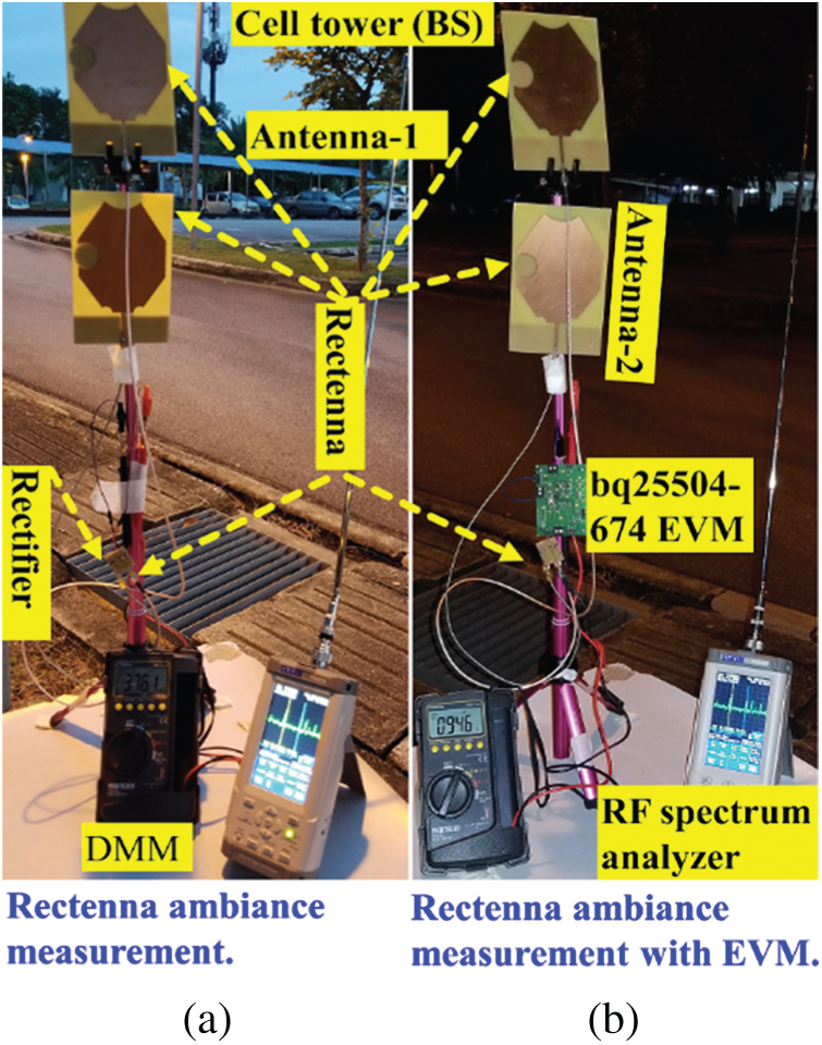
Figure 11: Rectifier ambiance measurement setups (a) Without EVM (Output dc voltage = 376.1 mV) (b) With EVM (Output dc voltage = 945 mV)
The results of the proposed dual-port five bands rectenna have shown an improvement concerning the RF-to-dc PCE and −10 dB operational bandwidth as compared to most of the previous related works from the literature. The proposed design demonstrates compactness and the ability to power a bq25504-674 EVM from the available ambient RF power signal.
In this work, a five-band dual-port rectifier has been proposed using an L-section and impedance transformer MN. The two IMN applied to the dual-port (Port-1 and Port-2) rectifier are matched at 0.94 GHz by Rectifier-1 and (1.80, 2.10, 2.46, and 2.63 GHz) through Rectifier-2. The proposed RF harvester realized a maximum measured RF-to-dc PCE and an output dc voltage of 72.70% and 154 mV for an input power of 3 dBm at 2.46 GHz. The circuit generates an output dc signal of 376.1 mV from the multitoned signal in the ambiance environment. The output voltage attained about 31% of the RF-to-dc PCE from the measured RF power density recorded by the spectrum analyzer. A low-powered bq25504-674 EVM integrated with the rectifier achieved an output dc voltage of 945 mV. The RF harvester shows a good performance at low input power and occupies a small section of the PCB at 0.20 λg × 0.15 λg. The wide operational bandwidth across the operating frequencies makes the proposed rectifier a fit candidate for low-powered RF applications.
Funding Statement: This work was supported by TM R&D Malaysia under Project Number MMUE/190001.
Conflicts of Interest: The authors declare that they have no conflicts of interest to report regarding the present study.
1. U. Muncuk, K. Alemdar, J. D. Sarode and K. R. Chowdhury, “Multiband ambient RF energy harvesting circuit design for enabling batteryless sensors and IoT,” IEEE Internet of Things Journal, vol. 5, no. 4, pp. 2700–2714, 2018. [Google Scholar]
2. C. R. Valenta and G. D. Durgin, “Harvesting wireless power: Survey of energy-harvester conversion efficiency in far-field, wireless power transfer systems,” IEEE Microwave Magazine, vol. 15, no. 4, pp. 108–120, 2014. [Google Scholar]
3. M. Mansour, X. Le Polozec and H. Kanaya, “Enhanced broadband RF differential rectifier integrated with archimedean spiral antenna for wireless energy harvesting applications,” Sensors, vol. 19, no. 3, pp. 655, 2019. [Google Scholar]
4. T. Soyata, L. Copeland and W. Heinzelman, “RF energy harvesting for embedded systems: A survey of trade offs and methodology,” IEEE Circuits and Systems Magazine, vol. 16, no. 1, pp. 22–57, 2016. [Google Scholar]
5. S. Muhammad, J. J. Tiang, W. S. Kin, A. Iqbal, M. Alibakhshikenari et al., “Compact rectifier circuit design for harvesting gsm/900 ambient energy,” Electronics, vol. 9, no. 10, pp. 1614, 2020. [Google Scholar]
6. C.-Y. Hsu, S.-C. Lin and Z.-M. Tsai, “Quadband rectifier using resonant matching networks for enhanced harvesting capability,” IEEE Microwave and Wireless Components Letters, vol. 27, no. 7, pp. 669–671, 2017. [Google Scholar]
7. M. M. Mansour and H. Kanaya, “Novel l-slot matching circuit integrated with circularly polarized rectenna for wireless energy harvesting,” Electronics, vol. 8, no. 6, pp. 651, 2019. [Google Scholar]
8. S. Shen, C.-Y. Chiu and R. D. Murch, “Multiport pixel rectenna for ambient RF energy harvesting,” IEEE Transactions on Antennas and Propagation, vol. 66, no. 2, pp. 644–656, 2017. [Google Scholar]
9. I. Adam, M. N. M. Yasin, H. A. Rahim, P. J. Soh and M. F. Abdulmalek, “A compact dual-band rectenna for ambient RF energy harvesting,” Microwave and Optical Technology Letters, vol. 60, no. 11, pp. 2740–2748, 2018. [Google Scholar]
10. F. Khalid, W. Saeed, N. Shoaib, M. U. Khan and H. M. Cheema, “Quadband 3D rectenna array for ambient RF energy harvesting,” International Journal of Antennas and Propagation, vol. 2020, Article ID: 7169846, 23 pages, 2020. https://doi.org/10.1155/2020/7169846. [Google Scholar]
11. B. L. Pham and A.-V. Pham, “Triple bands antenna and high efficiency rectifier design for RF energy harvesting at 900, 1900 and 2400 mhz,” in 2013 IEEE MTT-S Int. Microwave Symposium Digest, Seattle, WA, USA, pp. 1–3, 2013. [Google Scholar]
12. T. Skaik, “A quad-band rectifier design with improved matching bandwidth for RF energy harvesting applications,” in IEEE Int. Conf. on Promising Electronic Technologies, Deir El-Balah, Palestine, pp. 82–86, 2017. [Google Scholar]
13. S. Chandravanshi, S. S. Sarma and M. J. Akhtar, “Design of triple band differential rectenna for RF energy harvesting,” IEEE Transactions on Antennas and Propagation, vol. 66, no. 6, pp. 2716–2726, 2018. [Google Scholar]
14. J.-J. Lu, X.-X. Yang, H. Mei and C. Tan, “A four-band rectifier with adaptive power for electromagnetic energy harvesting,” IEEE Microwave and Wireless Components Letters, vol. 26, no. 10, pp. 819–821, 2016. [Google Scholar]
15. J. Liu and X. Y. Zhang, “Compact triple-band rectifier for ambient RF energy harvesting application,” IEEE Access, vol. 6, pp. 19018–19024, 2018. [Google Scholar]
16. C. Song, Y. Huang, J. Zhou, J. Zhang, S. Yuan et al., “A high efficiency broadband rectenna for ambient wireless energy harvesting,” IEEE Transactions on Antennas and Propagation, vol. 63, no. 8, pp. 3486–3495, 2015. [Google Scholar]
17. S. Shen, Y. Zhang, C.-Y. Chiu and R. D. Murch, “A triple-band highgain multibeam ambient RF energy harvesting system utilizing hybrid combining,” IEEE Transactions on Industrial Electronics, vol. 67, no. 11, pp. 9215–9226, 2019. [Google Scholar]
18. M. Pinuela, P. D. Mitcheson and S. Lucyszyn, “Ambient RF energy harvesting in urban and semi-urban environments,” IEEE Transactions on Microwave Theory and Techniques, vol. 61, no. 7, pp. 2715–2726, 2013. [Google Scholar]
 | This work is licensed under a Creative Commons Attribution 4.0 International License, which permits unrestricted use, distribution, and reproduction in any medium, provided the original work is properly cited. |