DOI:10.32604/cmc.2022.020426
| Computers, Materials & Continua DOI:10.32604/cmc.2022.020426 | |
| Article |
Reversible Logic Based MOS Current Mode Logic Implementation in Digital Circuits
1Department of Electronics and Communication Engineering, Sri Ramakrishna Engineering College, Coimbatore, India
2Department of Electronics and Communication Engineering, Anna University, Regional Campus, Coimbatore, India
*Corresponding Author: S. Sharmila Devi. Email: sharmilasmr@gmail.com
Received: 24 May 2021; Accepted: 07 July 2021
Abstract: Now a days, MOS Current Mode Logic (MCML) has emerged as a better alternative to Complementary Metal Oxide Semiconductor (CMOS) logic in digital circuits. Recent works have only traditional logic gates that have issues with information loss. Reversible logic is incorporated with MOS Current Mode Logic (MCML) in this proposed work to solve this problem, which is used for multiplier design, D Flip-Flop (DFF) and register. The minimization of power and area is the main aim of the work. In reversible logic, the count of outputs and inputs is retained as the same value for creating one-to-one mapping. A unique output vector set can be generated for each input vector set and information loss is also prevented. In reversible MCML based multiplier, reversible logic full adder is utilized to minimize the area and power. D flip-flops based on reversible MCML are often designed to store information that is then combined to form a reversible MCML based register. The proposed reversible MCML multiplier attains average power of 0.683~mW, Reversible MCML based DFF achieves 0.56 μW and Reversible MCML based 8-bit register attains 04.04 μW. The result shows that the proposed Reversible MCML based multiplier, Reversible MCML based D flip-flop and Reversible MCML based register achieves better performance in terms of current, power dissipation, average power and area.
Keywords: MOS current mode logic; reversible logic; multiplier; D flip-flop and register
The need for very high-speed low-power VLSI circuits is raised due to rapid increase in communication system’s transmission speeds [1]. Major two driving forces of this high-speed circuit development are high integration level for providing higher performance with lower cost and provision to implementation with low-power system-on-chip. The CMOS is the popular VLSI technology widely used in recent decades [2]. Although, scaling is used for enhancing CMOS technologies performance in a noticeable manner, applications power and speed requirements cannot be satisfied simultaneously by conventional CMOS circuit. Significant supply noise is generated by conventional CMOS circuits. Sensitive digital and analog circuit’s on-chip integration is hindered by conventional methods. MCML is a logic style, which can satisfy the need of high speed with minimized power consumption when compared with traditional CMOS circuits at these high frequencies [3]. The traditional Emitter Coupled Logic (ECL)’s benefits like common mode noise rejection, di/dt noise minimization, high speed without bipolar transistors requirement can be maintained in MCML. For supply noise, higher immunity is provided by MCML architecture because of its differential structure. Because of its minimized output voltage swing, cross talk is minimized and because of constant current flow in supply rails, noise generation also will be very low. A multiplier is one of the most important building block that is widely used in real-time Digital signal Processing (DSP). Multiplier block should be operated with low power, with minimized layout area while operating at high speed in real-time DSP processing task [4]. Now a days, the multiplier is implemented using both the CMOS [5], MCML logic styles [6] to improve the performance. In the past few decades, most promising research area is reversible logic and in various technologies like optical computing, low power CMOS and nanotechnology, they are used [7]. Garbage outputs count, circuits depth, quantum cost can be reduced by designing reversible logic. The inputs and outputs count are same in these reversible logic circuits. Between output and input vectors, there will be an one to one mapping [8–10]. From inputs, outputs can be computed using this and from outputs, inputs can be recovered uniquely using this. In different digital electronic circuits, to provide proper applications processing, basic units like Memory and registers are made using flip flops. One bit of information can be stored in one flip-flop [11,12]. There are four flip-flop types in basic namely, SR (“set-reset”), T (“toggle”), D~(“data”) and JK. In these flip-flop types, major difference are inputs count they have and how they change state. For each type, there are also different variations that enhance their operations. The most common flip-flop topology is the DFF [13], however the MCML implementation of a DFF suffers from transparency issues that cause it to act like a latch. Different digital circuits like registers, clock circuits, memory are designed using MOS Current Mode Logic circuits. Recent works are designed multiplier [14], flip flop [15,16] and registers using MOS Current Mode Logic circuits. However, it has only traditional logic gates that have issues with information loss. To overcome this problem, the proposed work integrates the reversible logic with MCML which is used for designing multiplier, D flip-flop and registers. The main contribution of the proposed research work is the reduction of area and power using reversible logic in designed circuits. This paper is structured as follows: Section 1 describes the information about Complementary Metal Oxide Semiconductor, MOS Current Mode Logic, multiplier and flip-flops. Then, Section 2 explains the technical details of the proposed Reversible Logic Based MOS Current Mode Logic Implementation. The simulation results are given in Section 3. Finally, Section 4 concludes this paper.
2.1 MCML Based Multiplier Design
The MCML multiplier is formulated by using MCML full adders. In MCML full adder, logic gates are performed based on the six input signals. In MCML multiplier design, the constant current source is used for reducing design complexity as well as for achieving better energy consumption. The MCML multiplier design is shown in Fig. 1.

Figure 1: Multiplier design using MCML logic
2.2 Reversible MCML Based Multiplier
The reversible MCML multiplier is designed by using reversible logic based full adder. For minimizing power dissipation and area, proposed research work uses reversible logic based full adder.
Reversible Logic Based Full Adder
Reversible logic is used for enhancing the significance of MCML full adder and by this logic, garbage output and gate counts are evaluated. According to six input signals, operation of logic gates is performed in the MCML full adder. In logic gates, changes have been carried out to achieve reversibility. In reversible gate, the input and output’s counts are equal. A one to one mapping is observed between output and input vectors. Using output vector’s states, input vector’s states can be reconstructed uniquely.
The MCML full adder based on reversible logic is shown in Fig. 2 [17]. One PMOS and nineteen NMOS are used in this proposed design. Outputs are derived according to the inputs. To perform the reversibility, fourth input is maintained as a constant in this circuit (D = 0). P represents the carry and Q represents the full adder sum. Output S and R is similar to input D and C. When compared with the available design of MCML full adder design, very less gate counts are required in proposed MCML full adder.
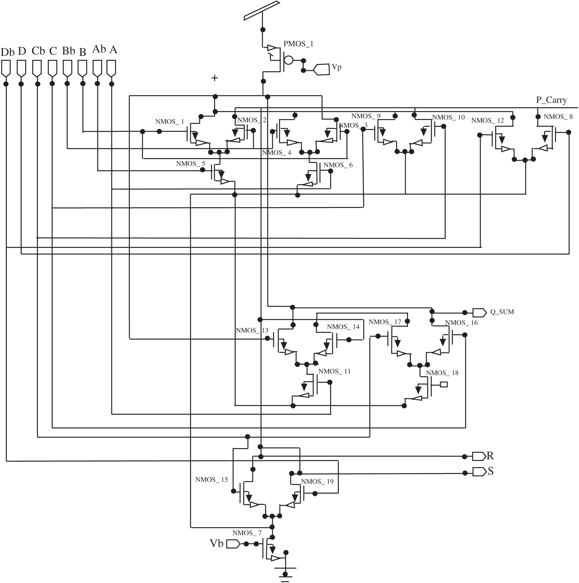
Figure 2: Schematic diagram of reversible logic based full adder
Reversible MCML Multiplier
The full adder is the significant component of reversible MCML multiplier. The reversible MCML multiplier is formulated using reversible logic based full adder. The reversible MCML multiplier achieves better performance due to its capability to retrieve the input data from output and minimizes heat dissipation and area. The schematic diagram of reversible MCML multiplier is shown in Fig. 3.
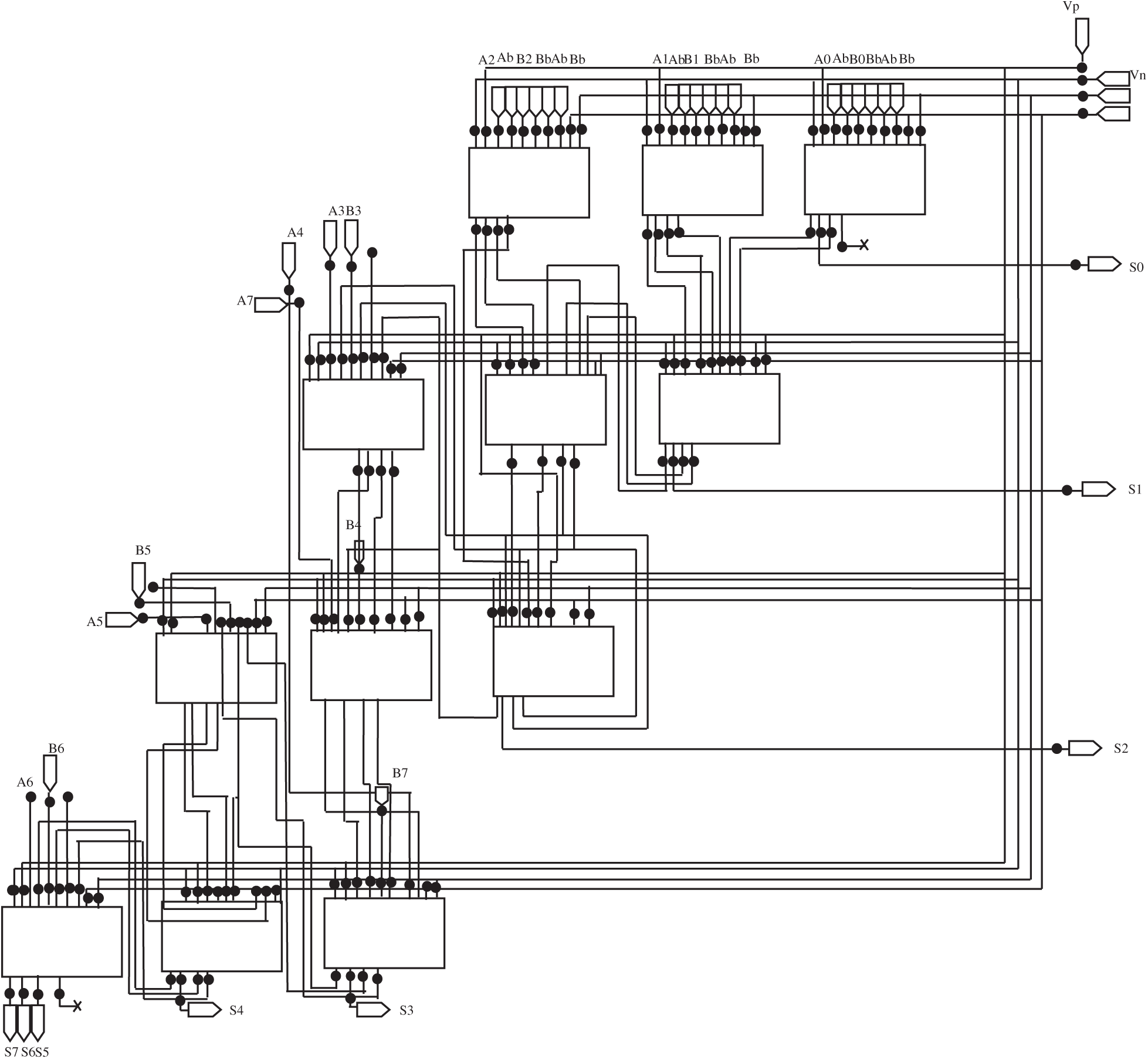
Figure 3: Schematic diagram of the reversible MCML multiplier
Flip flops are the basic tools to store digital data [18,19]. One bit of information can be stored in one flip-flop [20]. It is also utilized as data processor and memory storage elements.
There is an input D (data), input clock and outputs called Q and
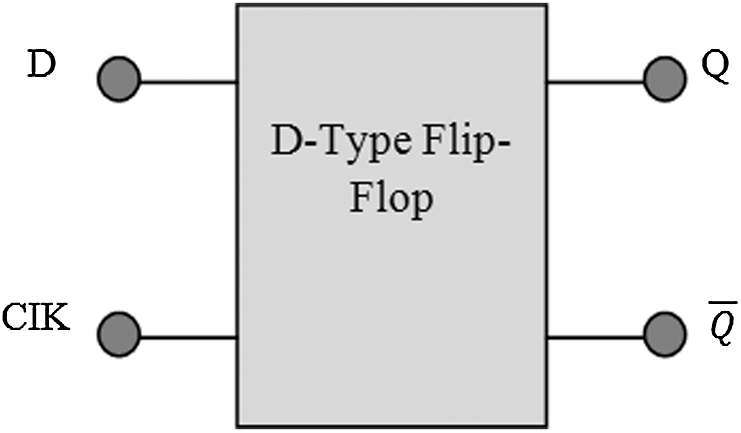
Figure 4: Pictorial representation of D-type flip-flop

The D type flip-flop is designed by using MCML. The operation of MCML D flip-flop is equivalent to the traditional D flip-flop. The conventional D flip-flop is implemented using CMOS technologies. The MCML D flip-flop is implemented using MCML technology to achieve area and power improvements. In MCML based D flip-flop circuit, two PMOS and seven NMOS transistors are used. And also clock is given as an additional input. Based on the clock and input D, the output is produced. Fig. 5 illustrates the circuit of MCML D flip-flop.
For minimizing power and area in MCML circuit, implemented the reversible logic in this proposed research work. Based on reversible MCML, the D flip-flop is designed. In this condition, huge power dissipation can be minimized using reversible logic in an effective manner. There are k number of output and k number of inputs in reversible logic design. These are benefits of reversible circuit over combinational circuits and it makes highly an effective one. The reversible MCML D flip-flop design is shown in Fig. 6.
The two PMOS and seven NMOS transistors are used in this proposed design. Outputs are derived based on inputs. After storing desired data, data input is isolated from flip flop’s latching circuitry using an additional input called “CLOCK” or “ENABLE” input. With the active clock input, D input condition is copied to output Q due to this. According to the input, there will be change in output.
The registers are synchronous circuits [21,22]. It is extensively used in almost all the applications to store the state information. An n-bit register has n flip-flops which are capable to store n bit binary information. A common clock is used for each flip-flop in the register. In this proposed work, MCML based flip-flops are combined to form a MCML based register. The schematic diagram of MCML based register is shown in Fig. 7.
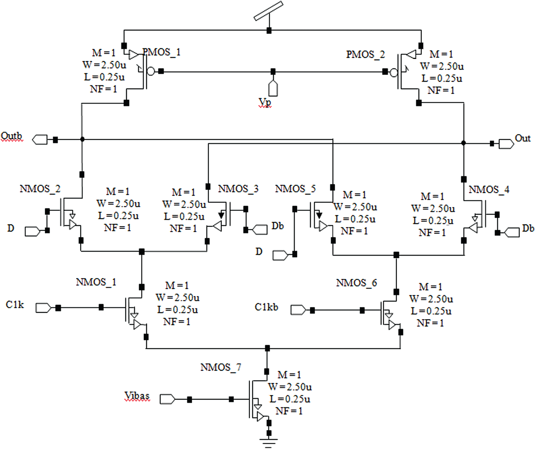
Figure 5: MCML based D flip-flop circuit
2.6 Reversible MCML Based 8-Bit Register
In this proposed research work, 8-bit register is designed for ultralow power design. The group of reversible MCML based flip-flops is combined to form a register. The schematic diagram of reversible MCML based register is shown in Fig. 8.
The 8-bit register holds an 8-bit logical value (i.e., 10110110), and it is formed by a collection of eight reversible MCML D flip-flops. In order to form a register from a collection of reversible MCML D flip-flops, the reversible MCML flip-flops must all run on the same clock signal.
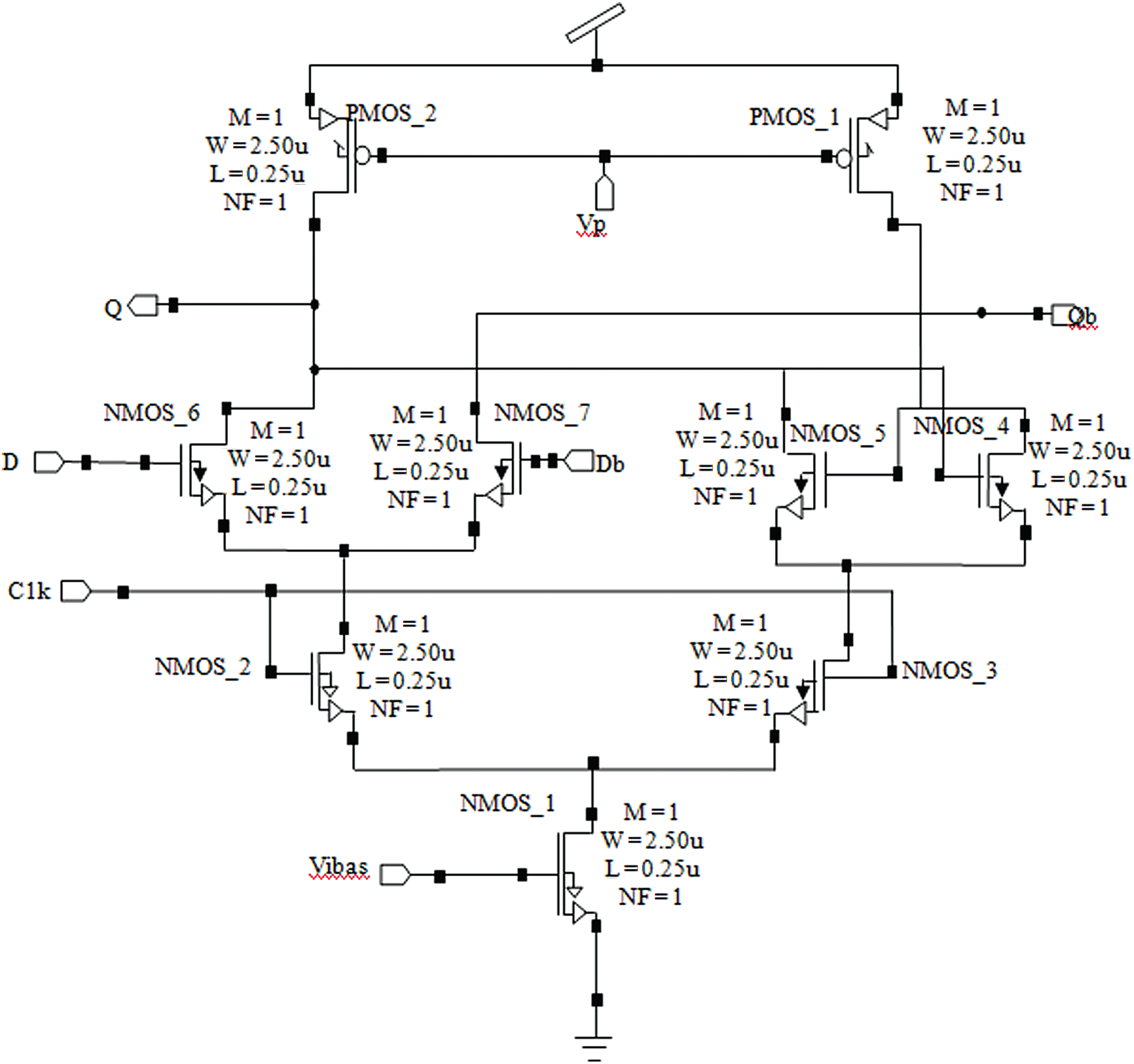
Figure 6: Reversible MCML based DFF
The MCML multiplier, Reversible MCML multiplier, MCML based DFF, Reversible MCML based DFF, MCML based 8-bit register and Reversible MCML based 8-bit register are implemented using Tanner EDA tool at 180 nm technology. The performance is analyzed in terms of static power dissipation, average power, static current and area. The simulation output of Reversible MCML based multiplier and Reversible MCML DFF circuits are shown in Figs. 9 and 10 respectively.
The simulation output of the reversible MCML based register is shown in Fig. 11. Tab. 2 summarizes the evaluation of the results of proposed Reversible MCML approach.
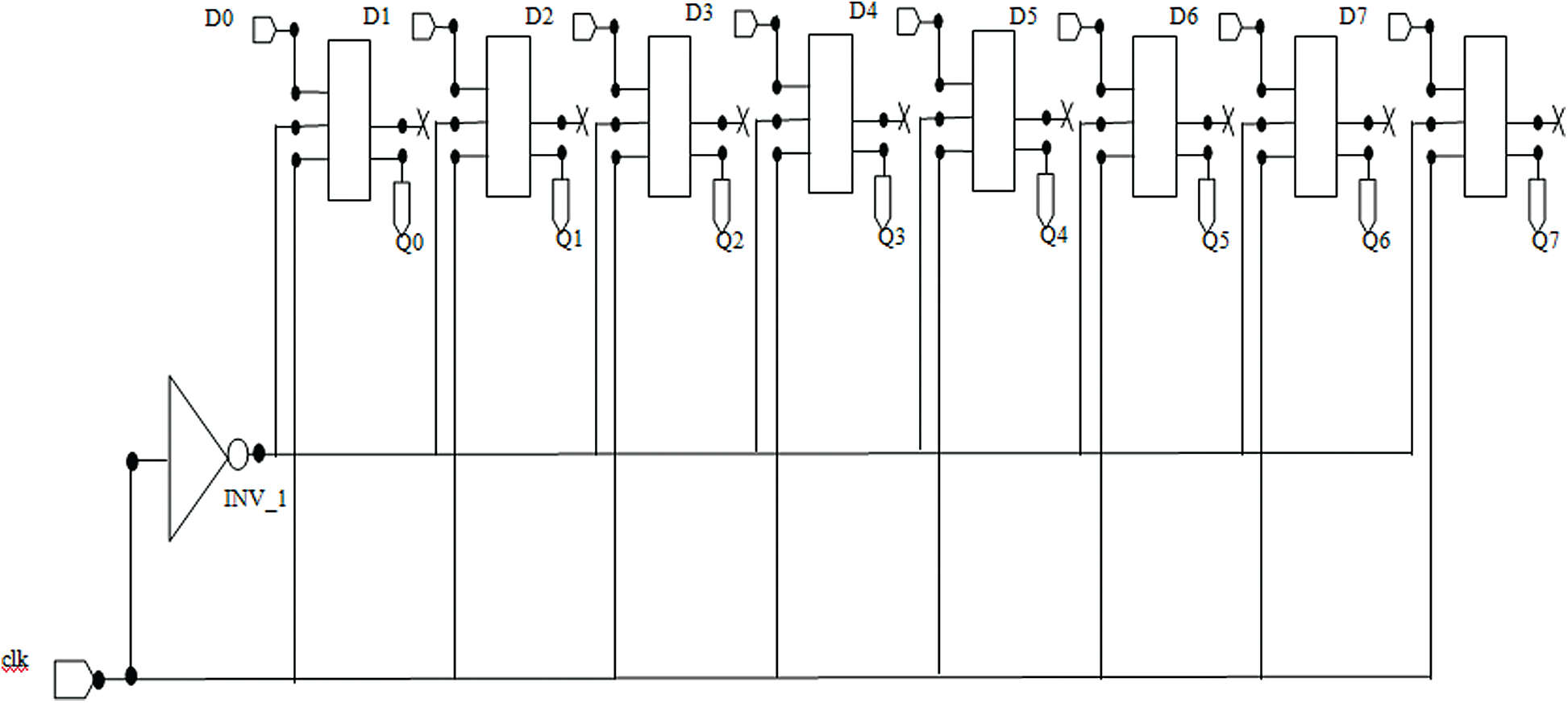
Figure 7: Schematic diagram of MCML based register

Figure 8: Schematic diagram of reversible MCML based register
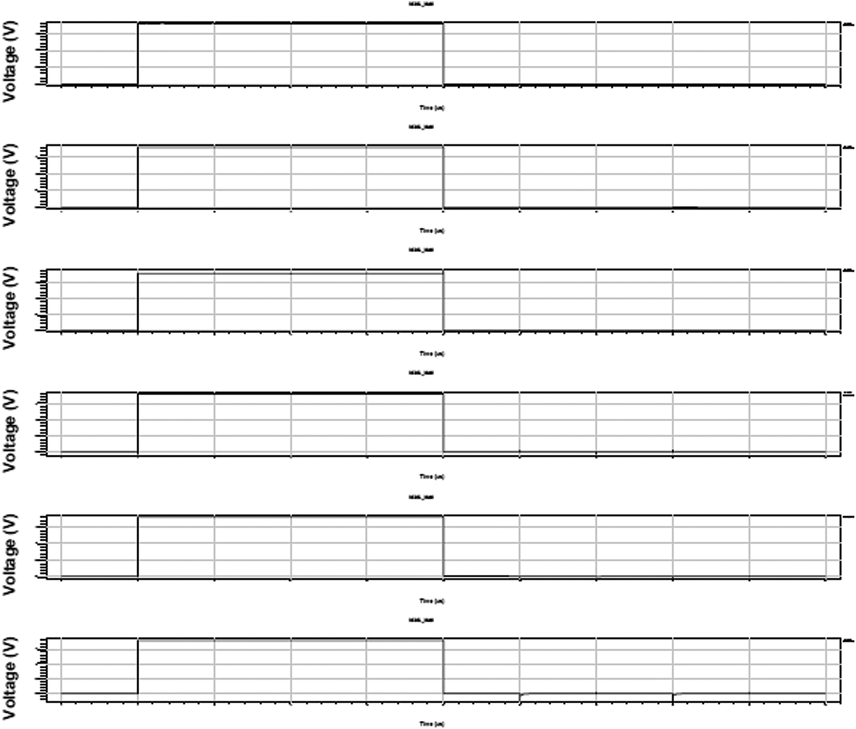
Figure 9: Simulation output of reversible MCML based multiplier
Fig. 12 shows the average power of MCML based multiplier, Reversible MCML based multiplier, MCML based DFF, Reversible MCML based DFF, MCML based 8 bit register and Reversible MCML based 8-bit register. In this proposed work, the reversible logic based circuits achieves minimum average power consumption due to its capability to retrieve the input data from output. The proposed reversible MCML multiplier attains 0.683 mW whereas MCML based multiplier achieves 6.19 mW. Average power of the Reversible MCML based DFF is 0.56μW when MCML based DFF attains 5.31 μW. The Reversible MCML based 8-bit register attains 04.04 μW whereas MCML based 8-bit register 8.29 μW.
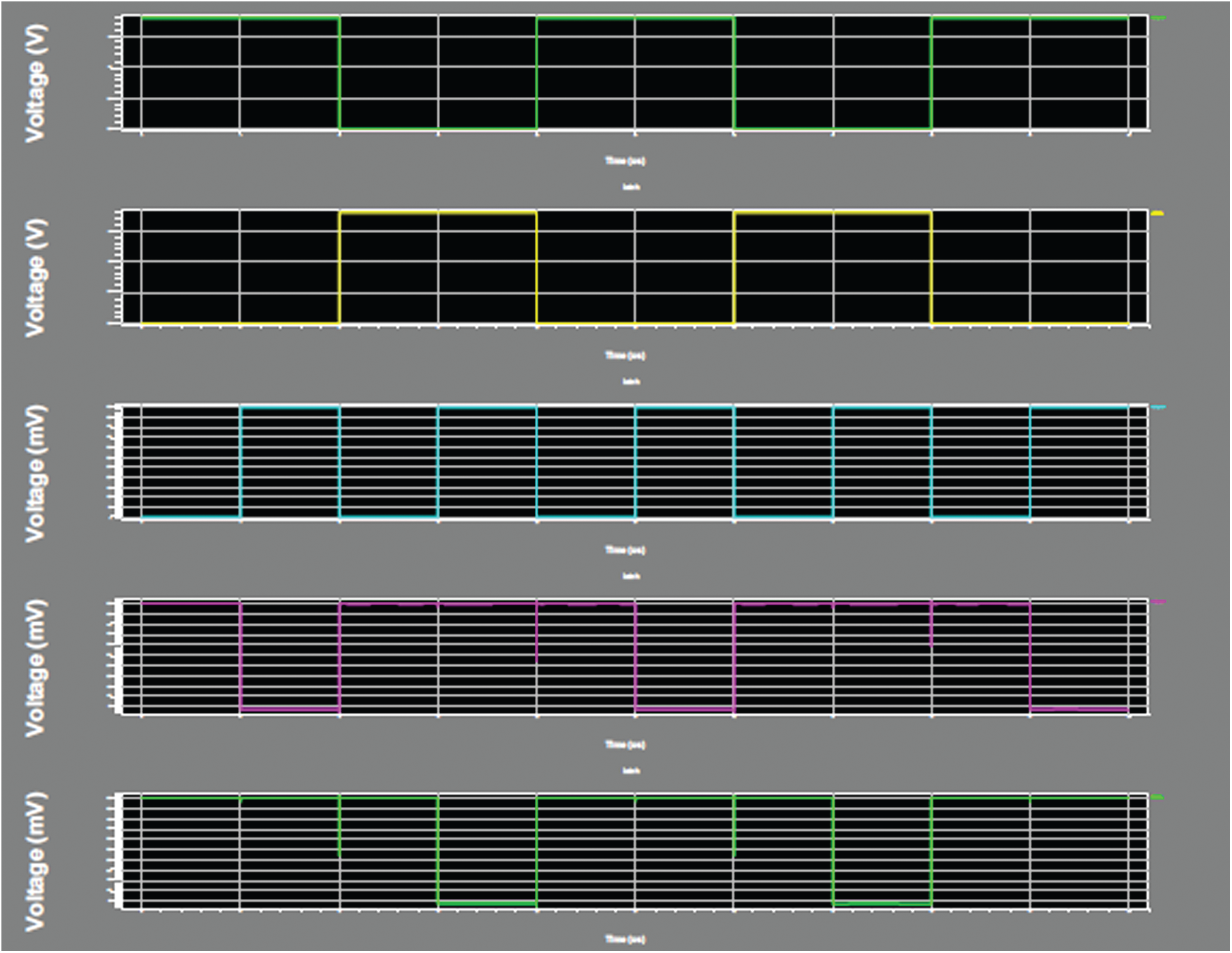
Figure 10: Simulation outputof reversible MCML based DFF
In Fig. 13, MCML based multiplier, Reversible MCML based multiplier, MCML based DFF, Reversible MCML based DFF, MCML based 8-bit register and Reversible MCML based 8-bit register are analyzed with respect to static power dissipation.
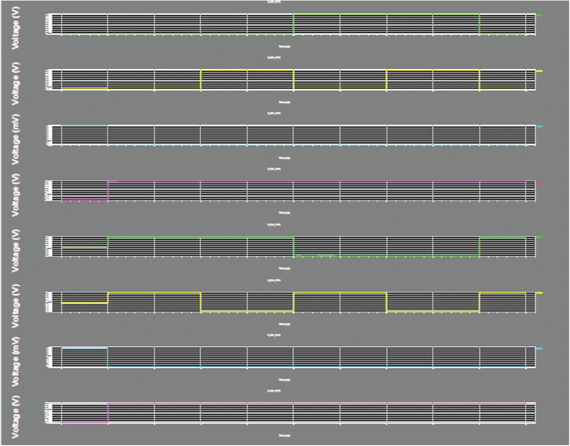
Figure 11: Simulation output of reversible MCML based register

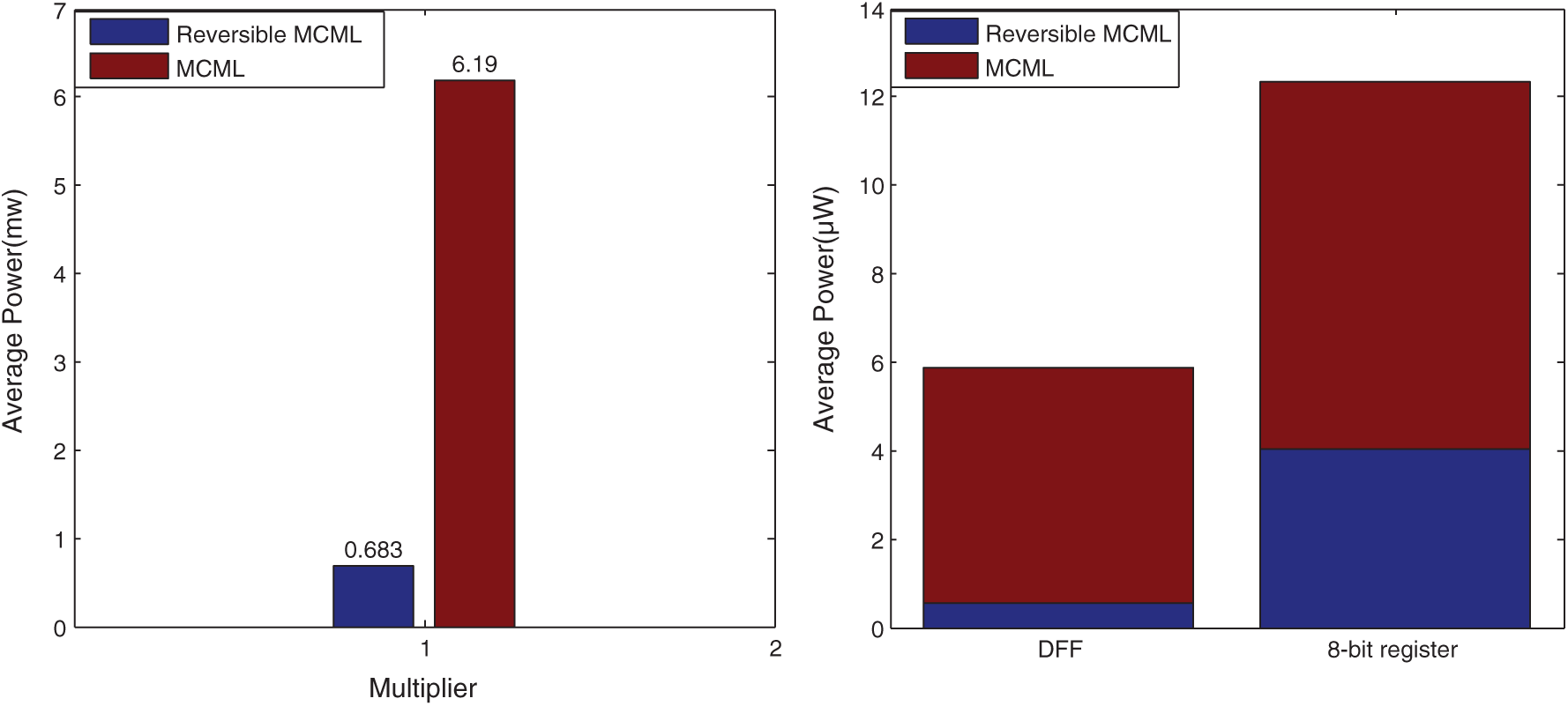
Figure 12: Average power consumption

Figure 13: Comparison for static power dissipation
The proposed Reversible MCML multiplier attains 97.2 nW of static power dissipation whereas MCML multiplier achieves 183.2 nW. The Reversible MCML based DFF’s static power dissipation is 1.25 μW when MCML based DFF attains 4.89 μW. The Reversible MCML based 8-bit register attains 1.19 μW whereas MCML based 8-bit register provides 11.85 μW.
The static current comparison of the MCML based multiplier, Reversible MCML based multiplier, MCML based DFF, Reversible MCML based DFF, MCML based 8-bit register and Reversible MCML based 8-bit register are shown in Fig. 14. The proposed reversible MCML multiplier attains 54 nA of static current whereas MCML based multiplier achieves101.7 nA. The static current of the Reversible MCML based DFF is 0.69 μA when MCML based DFF attains 2.71 μA. The Reversible MCML based 8-bit register attains 0.66 μA whereas MCML based 8-bit register achieves 6.58 μA. The experimental results show that the proposed reversible MCML achieves minimum static current than conventional MCML.
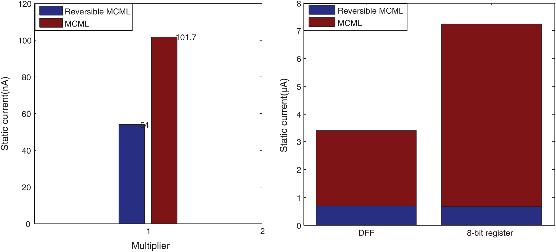
Figure 14: Comparison of static current
Area of the MCML based multiplier, Reversible MCML based multiplier, MCML based DFF, Reversible MCML based DFF, MCML based 8-bit register and Reversible MCML based 8-bit register are shown in Fig. 15. In this proposed work, area is reduced due to the function of reversibility. The proposed Reversible MCML has area of 240 whereas MCML multiplier has 458. Area of the Reversible MCML based DFF is 18 whereas MCML based DFF has 22. The Reversible MCML based 8-bit register has 144 whereas MCML based 8-bit register has 178. As shown in experimental results, the proposed reversible MCML achieves minimum area compared with MCML.

Figure 15: Area comparison
In this proposed research work, multiplier based on reversible MCML, reversible MCML based flip-flop and reversible MCML based register circuits are designed to achieve better area and power. The reversible logic is being used very fast because of its ability in designing a highly complex circuit with minimized power dissipation. The proposed circuit is implemented using Tanner EDA tool at 180 nm technology. From simulation outcome, it is be concluded that the area of proposed reversible MCML based multiplier is 240 which is 47.59% lower than MCML based multiplier, reversible MCML based flip-flop achieves 18.18% of area reduction th\-an MCML based DFF and reversible MCML based register attains 19.10% of area reduction than MCML based register. The performance of the MCML multiplier, Reversible MCML multiplier, MCML based DFF, Reversible MCML based DFF, MCML based 8-bit register and Reversible MCML based 8-bit register are evaluated in terms of static current, static power dissipation, average power and area. In future, reversible logic is applied in C-slow processor with FIFO memory. Here, the performance of processors is enhanced by exploiting multithreading technique in single core processors.
Acknowledgement: We show gratitude to anonymous referees for their useful ideas.
Funding Statement : The authors received no specific funding for this study.
Conflicts of Interest: The authors declare that they have no conflicts of interest to report regarding the present study.
1. H. Reyserhove and W. Dehaene, Efficient VLSI design flow. in Efficient Design of Variation-Resilient Ultra-Low Energy Digital Processor. Berlin, Germany: Springer, pp. 53–85, 2019. [Online]. Available at: https://link.springer.com/book/10.1007/978-3-030-12485-4. [Google Scholar]
2. P. Li, W. Xi, X. Yin, H. Yao and H. Chen, “Design of a CMOS lineal hall sensor front-end working in current mode with programmable gain stage for power specific chip,” Journal of Sensors, vol. 2021, no. 6618206, pp. 1–5, 2021. [Google Scholar]
3. I. Savidis, S. Kose and E. G. Friedman, “Power noise in TSV-based 3-D integrated circuits,” IEEE Journal of Solid-State Circuits, vol. 48, no. 2, pp. 587–597, 2013. [Google Scholar]
4. A. Kanhe, S. K. Das and A. K. Singh, “Design and implementation of low power multiplier using vedic multiplication technique,” International Journal of Computer Science and Communication, vol. 3, no. 1, pp. 131–132, 2012. [Google Scholar]
5. B. Preeti and S. S. Kerur, “Design and implementation of low power multiplier using VLSI techniques,” International Journal of Pure and Applied Mathematics, vol. 120, no. 6, pp. 767–785, 2018. [Google Scholar]
6. J. P. Joice, M. Anitha and I. R. Sheeba, “Design of filter using MOS current mode logic,” Bulletin of Electrical Engineering and Informatics, vol. 5, no. 1, pp. 72–78, 2016. [Google Scholar]
7. H. H. Radamson, H. Zhu, Z. Wu, X. He, H. Lin et al., “State of the art and future perspectives in advanced CMOS technology,” Nanomaterials, vol. 10, no. 8, pp. 1–86, 2020. [Google Scholar]
8. S. Singh, A. Choudhary and M. K. Jain, “A brief overview of reversible logic gate and reversible circuits,” International Journal of Electronics Engineering, vol. 11, no. 2, pp. 86–104, 2019. [Google Scholar]
9. E. P. A. Akbar, M. Haghparast and K. Navi, “Novel design of a fast reversible Wallace sign multiplier circuit in nanotechnology,” Microelectronics Journal, vol. 42, no. 8, pp. 973–981, 2011. [Google Scholar]
10. P. Biswas, N. Gupta and N. Patidar, “Basic reversible logic gates and it’s QCA implementation,” International Journal of Engineering Research and Applications, vol. 4, no. 6, pp. 12–16, 2014. [Google Scholar]
11. J. C. Jeon, “Low-complexity QCA universal shift register design using multiplexer and D flip-flop based on electronic correlations,” The Journal of Supercomputing, vol. 76, no. 8, pp. 6438–6452, 2020. [Google Scholar]
12. H. Singh, M. Meenalakshmi and S. Akashe, “Design and optimization of power efficient shift register using five-transistor based d-flip flop,” Journal of Active & Passive Electronic Devices, vol. 13, no. 4, pp. 271–279, 2018. [Google Scholar]
13. M. N. Divshali, A. Rezai and A. Karimi, “Towards multilayer QCA SISO shift register based on efficient D-FF circuits,” International Journal of Theoretical Physics, vol. 57, no. 11, pp. 3326–3339, 2018. [Google Scholar]
14. J. B. Kim and Y. S. Lee, “Design of a low-power 8 × 8-bit parallel multiplier using MOS current mode logic circuit,” International Journal of Electronics, vol. 94, no. 10, pp. 905–913, 2007. [Google Scholar]
15. K. K. Mandrumaka and F. Noorbasha, “Design of low voltage D flip-flop using MOS current mode logic (MCML) for high frequency applications with EDA tool,” IOSR Journal of VLSI and Signal Processing, vol. 7, no. 4, pp. 9–14, 2017. [Google Scholar]
16. M. Maiti, A. Paul, S. K. Saw and A. Majumder, “A dynamic current mode Dflip-flop for high speed application,” in Int. Conf. on Electronics, Materials Engineering & Nano-Technology, Kolkata, India, pp. 1–3, 2019. [Google Scholar]
17. S. Sharmila Devi and V. Bhanumathi, “Design of reversible logic based full adder in current-mode logic circuits,” Microprocessors and Microsystems, vol. 76, pp. 1–10, 2020. [Google Scholar]
18. M. Ramachandran, S. Prince, A. Kambham and N. Maruthi, “Design and simulation of all optical shift registers using D flip-flop,” Microwave and Optical Technology Letters, vol. 62, no. 7, pp. 2427–2438, 2020. [Google Scholar]
19. A. Saxena, M. Kaur, H. Pahuja and V. Chhabra, “Design and performance analysis of CMOS based D flip-flop using low power techniques,” International Journal of Research in Electronics and Computer Engineering, vol. 5, no. 4, pp. 216–225, 2018. [Google Scholar]
20. P. G. Dhoble and A. D. Kale, “A review paper on design of positive edge triggered D flip-flop using VLSI technology,” International Journal of Engineering Research Technology, vol. 3, no. 2, pp. 1512–1515, 2014. [Google Scholar]
21. Y. Bai, Y. Song, M. N. Bojnordi, A. Shapiro, E. G. Friedman et al., “Back to the future: Current-mode processor in the era of deeply scaled CMOS,” IEEE Transactions on Very Large Scale Integration Systems, vol. 24, no. 4, pp. 1266–1279, 2015. [Google Scholar]
22. T. Dua, V. K. Barodiya, V. Arya and N. Choudhary, “High-speed set D flip-flop design for portable applications,” in Proc. of Integrated Intelligence Enable Networks and Computing, Singapore, Springer, pp. 811–822, 2021. [Google Scholar]
 | This work is licensed under a Creative Commons Attribution 4.0 International License, which permits unrestricted use, distribution, and reproduction in any medium, provided the original work is properly cited. |