DOI:10.32604/cmc.2022.020623
| Computers, Materials & Continua DOI:10.32604/cmc.2022.020623 | |
| Article |
Exploring the Approaches to Data Flow Computing
1Department of Electrical and Computer Engineering, Technical University of Munich, Arcisstrasse 21, 80333 Munich, Germany
2Department of Computer Science, CCSIT, King Faisal University, 31982, Al Ahsa, KSA
*Corresponding Author: Abdul R. Khan. Email: raoufkhan@kfu.edu.sa
Received: 31 May 2021; Accepted: 03 September 2021
Abstract: Architectures based on the data flow computing model provide an alternative to the conventional Von-Neumann architecture that are widely used for general purpose computing. Processors based on the data flow architecture employ fine-grain data-driven parallelism. These architectures have the potential to exploit the inherent parallelism in compute intensive applications like signal processing, image and video processing and so on and can thus achieve faster throughputs and higher power efficiency. In this paper, several data flow computing architectures are explored, and their main architectural features are studied. Furthermore, a classification of the processors is presented based on whether they employ either the data flow execution model exclusively or in combination with the control flow model and are accordingly grouped as exclusive data flow or hybrid architectures. The hybrid category is further subdivided as conjoint or accelerator-style architectures depending on how they deploy and separate the data flow and control flow execution model within their execution blocks. Lastly, a brief comparison and discussion of their advantages and drawbacks is also considered. From this study we conclude that although the data flow architectures are seen to have matured significantly, issues like data-structure handling and lack of efficient placement and scheduling algorithms have prevented these from becoming commercially viable.
Keywords: Processor architecture; data flow architectures; Von-Neumann model; control flow architectures
With the increase in applications that demand high computational power while being power efficient, the need for efficient parallel computing resources in general purpose, as well as application specific processors, has increased manifold recently. The traditional Von-Neumann architecture is inherently sequential as it employs the program counter, and sequences through the program instructions. Although, a number of parallel processing techniques are deployed in the modern Von-Neumann processors, there are still applications like those in signal processing, network processing etc. which are inherently parallel in nature. To exploit this inherent parallelism, a contrasting processing paradigm, called data flow processing was proposed and the early proponents of this model of computation believed that it would provide extensive computing power and could replace the traditional control-flow architecture.
Data flow computing provides a few major advantages over control flow for parallel processing. Firstly, the data flow model is asynchronous where instruction execution is determined by the availability of operands hence providing an implicit synchronization of parallel instructions. Secondly, the data flow graph representation eliminates the need for explicit management of parallel execution of program by exposing the inherent parallelism of the application.
The first proposals for data flow machines were made in the 70s [1,2]. In the following decades, a number of other proposals for such processors were made; however, most of these were based on distributed set of processing elements (PEs) and given the costs of implementing large PEs on silicon, none of these were economically viable. There was a renewed interest in data flow computing in the early 2000s, and some of the proposed designs included support for imperative languages [3,4]. Furthermore, to overcome the inefficiencies in the pure data flow processors, there was a shift towards adopting a hybrid model which combined both Von-Neumann and data flow models. Although, data flow processing has been adopted in some accelerators, to the best of our knowledge, there has been no commercially viable general-purpose data flow processor till date. This is because of some of the key issues in this model of computation like efficient allocation of data flow graphs still require additional research [5].
In this paper, we explore the most prominent data flow architectures proposed till date. The aim of the paper is to provide a comprehensive review of the data flow processor architectures that provide an alternative to the conventional Von-Neumann processor. The data flow architectures, even though promising, have failed to become commercially successful and have been limited to academic research. This paper analyses the drawbacks of the various previously proposed architectures, which have proved to be an impediment in the progress of the dataflow architecture towards a mature technology. A few of the remaining challenges are highlighted which may facilitate the future research work in this particular area.
The paper is organized as follows. First, we begin with a brief conceptual overview of the two programming models in the second section. In the third section, the data flow processors proposed in the literature are described in terms of their micro-architecture and execution model and are accordingly categorized. A comparative discussion of the most prominent features of these processors is done in the fourth section. Finally, the last section concludes the work and identifies a few future directions in the design of data flow processors.
2 Control Flow and Data Flow Architectures
This section covers the preliminaries and basic concepts behind the two contrasting computing models.
The control flow or commonly referred to as the Von Neumann architecture is the most successful and commercially viable computing model prevalent till date. It mainly consists of a processing unit for computation, a control unit for loading the instructions, memory system for storing data and instructions and an input/output interface. One of the defining features of this architecture is the program counter (PC), which is a register used to transfer the control between instructions. The PC enforces a sequence on the instruction in which the program is to be executed by holding the value of the instruction address that shall be executed next. The PC gets the next address either by automatically incrementing the previous address or could be directed explicitly by means of a branch or jump instruction.
The sequential execution of programs in this architecture leads to memory ordering schemes that define the order in which the memory operations occur, that is, according to the order in which they were fetched. All the imperative programming languages are built with these memory semantics taken into consideration. As a consequence, all the programs have to be written in a manner which enforces this sequential execution even if there is no inherent sequential execution requirement in the program. This, along with other hazards, leads to underutilization of hardware resources and throughput bottleneck and is a major drawback of this architecture.
Fig. 1 depicts the execution of a simple computation in a control-flow manner. The program counter is incremented and at each increment performs the corresponding computation. Assuming all the initial operands are independent, this restricts parallelism as the two addition operations could have been performed in parallel. To overcome this issue several techniques are employed to exploit the parallelism in the programs at different granular levels. This could be Instruction-Level Parallelism (ILP) e.g., Instruction pipelining and Out-of-order execution, Thread-Level Parallelism (TLP) e.g., multi-threading, or Data-Level Parallelism (DLP).
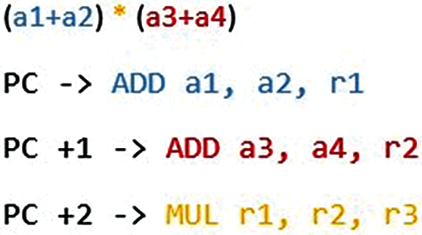
Figure 1: Execution of a simple computation in a control flow manner using a program counter
The data flow architecture provides a completely contrasting computing model to the conventional Von-Neumann architecture. It eliminates the need of the program counter, as the instructions are no longer executed in a sequential manner. This architecture provides the means to exploit the inherent parallelism in a program. The execution in a data flow machine is driven by the availability of operands and the execution resource. That is, an instruction ‘fires’ as soon as the operands arrive at a free execution node of the hardware. As such, if all the operands corresponding to multiple instructions become available, they can be executed in parallel. The programs are represented by means of a data flow graph (DFG),
Taking the example defined in the previous section the corresponding DFG can be represented as shown in Fig. 2. Each of the node of the DFG will fire as soon as its operands arrive. As such, the two addition operations would execute in parallel.
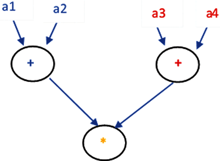
Figure 2: Data flow graph representation of the computation
The data flow machines are traditionally classified as Static and Dynamic data flow [6]. The static data flow allows only one token per arc that is; only a single instance of an instruction can be executed at once [1,7–9]. The Dynamic version on the other hand allows multiple tokens belonging to different instances of the instructions per arc, where each token is tagged with the instance number. Hence, it is also referred to as tagged-token data flow machine [10–12].
3 Classification of Data Flow Architectures
In this section, we aim to classify the recently proposed data flow processors. The classification is done in a hierarchical manner. First, we broadly classify the architectures into two groups based on execution model, that is, whether they implement an exclusive data flow execution or combine the control-flow and data flow techniques to follow a hybrid model. Next, within the hybrid model we further classify the architectures based on whether the scheduling scheme implements the data flow and control-flow execution on a unified hardware substrate or statically offloads the data flow portion to a separate unit.
3.1 Exclusively Data Flow Architectures
The first category of data flow architectures consists of those, which exclusively implement the data flow execution model. These are generally aimed at replacing the Von-Neumann architecture in general purpose computing. The first proposal for such a machine was proposed by Dennis and Misunas [1] in 1974, and in the following decades a number of such machines were proposed [7,10,11,13]. However, none of these architectures could realize the true potential expected out of a data flow machines due to issues like memory programming difficulties, token matching overhead etc. More recently, a few new proposals have been made and two of them are discussed in detail below.
WAVESCALAR: The Wavescalar is a dynamic data flow machine that is comprised of a distributed set of PEs which are hierarchically organized into tiles. It was proposed by a team at the University of Washington in 2003 [14].
Architecture Overview: The Wavescaler programs are executed on a tile-based distributed network of processing elements called the WaveCache as shown in Fig. 3. The processing element implements a 5-stage execution pipeline consisting of these stages - Input, Match, Dispatch, Execute, and Output. Two PEs are grouped together to form a pod, which communicate the ALU results via a common bypass network. Four such pods together form a domain, and four domains together for a cluster. The cluster can be regarded as the basic building block of the WaveCache as several such clusters can be connected together in a 2- dimensional mesh network to form a scalable processing substrate. The PEs inside a domain communicate by means of a pipelined bus, while as the inter-domain communication occurs via a pseudo-PE called NET pseudo-PE. A similar pseudo-PE, called MEM pseudo-PE is used as a gateway for memory operations for each domain. The inter-cluster communication is packet-based, and each cluster contains a network switch, which routes the messages from six ports – four for North, East, South, and West directions, one for store buffer and L1 data cache and one is shared among the NET PEs of the domains within the cluster.
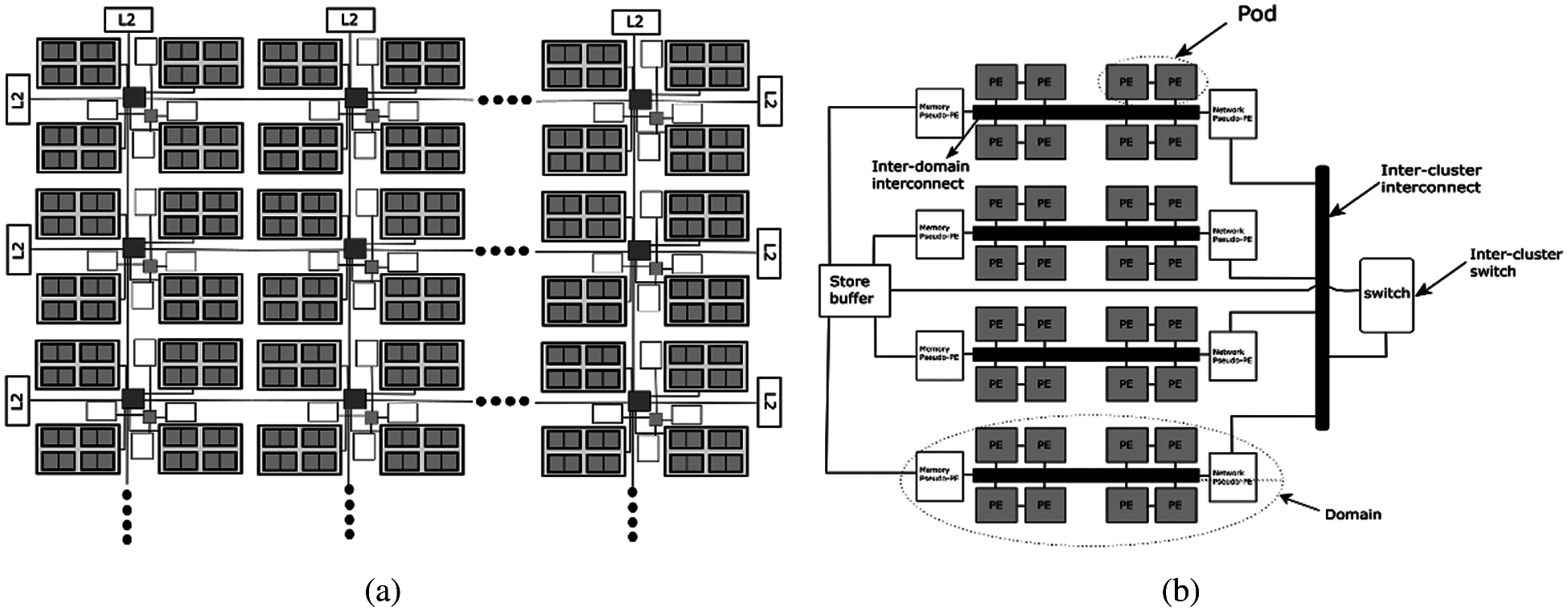
Figure 3: Wavecache Architecture [14]. (a) Tile view, (b) Cluster view
Each cluster has one store Buffer, which is responsible for enforcing the memory-ordering scheme, called the Wave-ordered memory. It works by dividing the program into waves, and within each wave the memory access instructions are annotated to enforce the memory sequence. As such, the ordering works at two levels – coarse grain by means of wave numbers, and fine grain by means of instruction annotations [3]. From the programming perspective each instruction has a dedicated PE, however, for practicality, a set of 64 instructions are dynamically assigned to each PE. As the working set of instructions changes, the Wavescalar replaces the unused instructions with new ones.
Execution Model: The key aspect of WaveScalar ISA is that it supports the conventional load/store semantics and hence can execute programs written in imperative languages. A program on a Wave-Scalar is executed in forms of ‘Waves’, which are basically acyclic and directed portions of the DFG. The compilation step includes the conventional steps like optimization and parsing and additionally the transformation to make the graph suitable for execution on Wavecache. It includes decomposing the graph into waves. Waves are similar to ‘hyperblocks’, and the data that traverses through the waves is annotated with the corresponding wave number, which are incremented using the ‘WAVE-ADVANCE’ instructions. This allows the instructions to operate on the different instances of the instructions.
To enforce memory ordering, the Wave-scalar annotates the memory instructions within a wave with sequence numbers resulting in a chain of operations. For example, Fig. 4 shows a simple load store sequence with the corresponding sequence numbers. The first element is the sequence number of the predecessor, the second is that of the instruction itself, and the last one is that of the successor. The ‘.’ Symbol represents that there is no predecessor or successor instructions, e.g., in the case when the instructions are first or last respectively. The sequence numbers are assigned in increasing order, such that the instruction with the larger number should be executed after the instruction with the smaller sequence number. In cases where there are a number of predecessor or successor paths, a wild card symbol ‘?’ is employed.
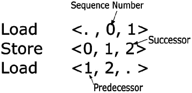
Figure 4: Simple Wave-ordered annotations
In order to ensure that there is a complete chain of memory operations along every path, a MEMORY-NOP instruction is used in places where there are no memory operations in a path of a branch. Furthermore, independent memory operations are annotated with a ripple number to allow parallel execution. Along with the wave-ordered memory, the Wavescalar also provides support for an unordered memory access scheme to avoid any unnecessary ordering of memory instructions, and both can be used interchangeably within the same graph as well as the same wave.
3.2 Hybrid Data Flow/Control-Flow Architectures
As mentioned in the earlier sections, both the Von-Neumann as well as exclusively data flow machines have their drawbacks and strengths. While the former is simple to implement and well suited for sequential applications, the latter is useful for exploiting the maximum parallelism. As such, to combine the benefits of the two different approaches, several proposals were made which employ a combination of both the models [4,5,15–17]. Some of these employ control flow execution between ‘execution blocks’ and data flow execution within the blocks e.g., Tera-op, Reliable, Intelligently adaptive Processing System (TRIPS) [4], Dynamically Specialized Execution Resource (DySER) [15] and Tartan [16]. On the other hand, other architectures schedule the blocks in a data-driven manner, while the instructions within a block are scheduled in a control flow manner e.g., MT-Monsoon [17], Task Superscalar [5]. Based on the separation of the two execution models on the hardware, we further divide these into two categories as follows.
In a conjoint architecture, a program is scheduled using both data flow and control flow scheduling on a single execution substrate as both the models are inherent to the architecture. This means that there is no scope for executing an application which could benefit from using either control-flow or data flow exclusively.
TRIPS: TRIPS is a dynamic, tile-based data flow architecture, which implements the Explicit Data Graph Execution (EDGE) ISA. It was proposed at University of Texas, Austin in 2003 [4].
Architecture Overview: TRIPS processor chip consists of three main components – the processors cores, the integrated L2 cache organized into a number of tiled banks (M tiles), and a lightweight routing network (N tiles) as shown in Fig. 5. Within each processor core, is a 4

Figure 5: TRIPS architecture [4]
Execution Model: The TRIPS compiler partitions the program into ‘hyperblocks’, where each block consists of 128 instructions and behaves as a ‘megainstruction’. These blocks are scheduled in a control flow mode, and the instructions within the block and executed in a data-driven manner with direct communication between the instructions. Hence, it can support imperative languages without much modification.
The blocks are statically scheduled to the computation blocks such that the dependencies between the instructions is explicitly expressed. Within a block, each instruction sends its result to the consumer instructions and as soon as all the operands at the instruction arrive, it fires. As such, each TRIPS instruction only specifies the target locations of the results, which are statically determined by the compiler.
To exploit more ILP, it provides support for up to 8 blocks of instructions to be executed simultaneously. That is, the G-tile can predict the next block of instructions, while it fetches and maps a block onto the execution array. The GT fetches the blocks by using its branch predictor, where it obtains the predicted block address and then uses the I-cache tags. If it hits, the block address is broadcasted to the I-cache banks, where each of them streams the block instructions into the execution array for their corresponding rows.
3.2.2 Accelerator Style Architectures
In data flow accelerator-style architectures, only a portion of the application is executed in a data flow fashion. The decision on which portion to accelerate is mostly static and is either taken by the programmer by means of application profiling or statically determined by the compiler. Furthermore, in some cases it is possible that the entire application may be executed without the data flow accelerator. We discuss two examples of such architectures in the following sub-sections.
DySER: The Dynamically Specialized Execution Resource (DySER) architecture aims to combine both parallelism and functional specialization. It was proposed in 2012 at the University of Wisconsin – Madison [15].
Architecture Overview: DySER works in conjunction with a general-purpose processor and is designed to be integrated into the execution phase of the pipeline as shown in Fig. 6. It consists of a 2-dimensional array of heterogeneous Functional Units (FU). Each FU is connected to four simple switches (S), which form a circuit-switched network, delivering the data and control instructions into and out of the FUs by forming configurable data-paths. The FUs are configured by means of a configuration register, to perform a specific function and read its inputs from a specific switch. The pipelining is implemented by means of a credit-based flow control. The validity of the data at each FU is checked by means of forward ‘valid’ signal and a backward ‘credit’ signal asserts the possibility of accepting a new data. For this purpose, the FUs also include the data and status registers. The configuration of DySER takes 64 cycles, and once configured it can be used multiple times for a given application phase.
The communication with the host processor is enabled via a set of named I/O ports which correspond to FIFO buffers that deliver the data in and out of the switches. The RISC ISA is extended by five instructions for enabling DySER configuration and the communication of register and memory data between the host and the accelerator.
Execution Model: The DySER compiler profiles the application to extract the commonly re-used ‘accelerable’ portions of the program and explicitly partitions the program into phases. The assumption is made that for a given program phase, only a few data flow blocks are active which are invoked multiple times. The DySER block is then configured to execute the DFG, before it is encountered. The register values are then sent to block or data is directly loaded from memory for each instance of the graph. This portion of the graph consisting of memory accesses is called ‘invocation slice’ and the remaining portion with computation operations is called the ‘computation slice’. This separation enables the usual memory optimizations to be implemented without hurdles. As the data arrives at DySER, it is routed through the block as per the determined configuration in a data flow manner. It can also speculatively invoke the next instance of the configuration and pipeline their execution.

Figure 6: DySER architecture and integration into execution pipeline [15]
PLUG: The Pipeline Look-Up Grid (PLUG) is an application specific data flow accelerator designed for optimally performing data structure lookups in a network processor. It was proposed at the University of Wisconsin-Madison in 2010 [16].
Architecture Overview: As with other tile-based architectures, the PLUG tile consists of three regions – processing Cores (
The On-Chip network is very simple and requires no buffering or flow control. Again, contention-free routing is made possible by making use of certain code-generation rules. A restricted multi-cast is employed, whereby the message is delivered to all the nodes appearing on the path to the final destination and the compiler makes sure that the all the multi-cast targets fall on the route when multicast is required.
The

Figure 7: PLUG architecture [16]. (a) Tile organization, (b) Single tile partitioned into three virtual tiles
Execution Model: The PLUG architecture works on the concept of transforming the data-structure lookups into a structured pipeline of memory and computation operations. It exploits the inherent structure of the lookup data-structure by mapping the data-structure to on-chip tiled storage. The parts of the data-structure representing one logical level are grouped to form a big ‘logical page’ with portions of the code, called Code-blocks, associated with each logical page. These code-blocks are agnostic to each other and perform the memory accesses independently within the scope of their own logical pages. Furthermore, they determine the next logical page that should be looked up next which results in a network message, which in turn, triggers the execution of another code-block. These logical pages are mapped to physical resources, after being explicitly portioned to match the storage space of the given tile. As such, these code-blocks associated with each logical page represent the nodes of the DFG and execution of programs is data flow driven by messages sent from tile to tile.
Besides generating the assembly code for the code-blocks, the compiler is also responsible for partitioning the logical pages into smaller physical pages, which can then be mapped to the specific tiles. The logical pages are generally lists of data-blocks, and the compiler simply divides these into equal sized chunks such that these are small enough to fit in a single memory. To map the DFG to PLUG chip, a greedy scheduling algorithm is employed which does a breadth first traversal and assigns them to the tiles which are ranked based on the distance from the reference point (Input port). Moreover, the compiler also has the responsibility to assign the DFG arcs to the On-chip network for which a graph-coloring approach is employed.
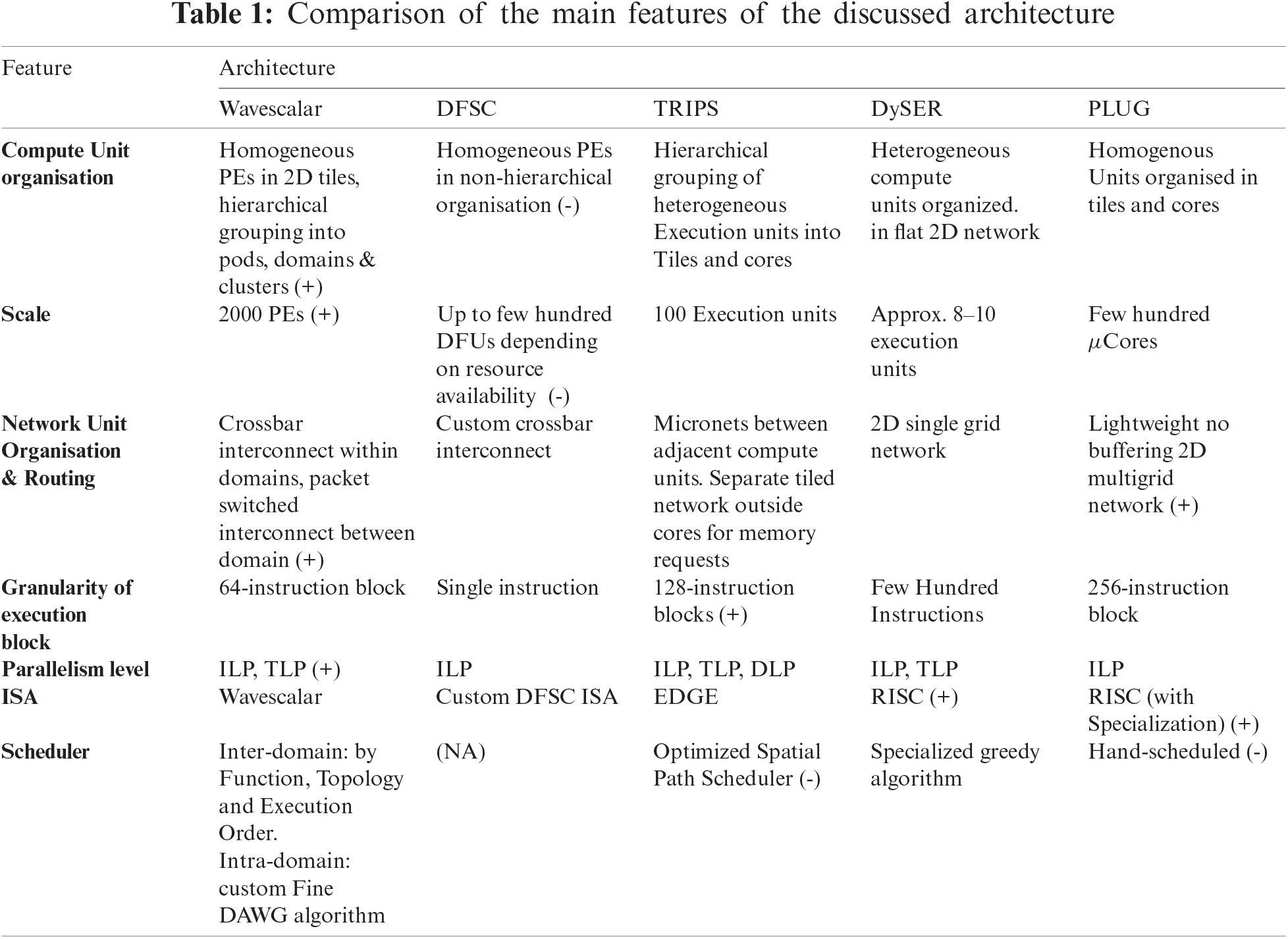
In this section we compare the above-mentioned architectures and broadly discuss their advantages and drawbacks. Tab. 1 summarizes the main features of these architectures. Features which present advantages are marked with (+) and those that are disadvantageous are marked with ( −). The advantages and disadvantages are discussed in the text.
4.1 Exclusively Data Flow Architectures
The Wavescalar is the most prominent architecture belonging to this class. Another recent FPGA-based architecture was proposed, called the Data Flow Soft Core (DFSC) in 2016 [18]. While the Wavescalar is aimed to be a general-purpose processor, the DFSC on the other hand is designed for accelerating scientific computations. The first architectural difference between the two lies in the organization of the compute and routing resources. While the Wavescalar groups the PEs in a hierarchical manner with different interconnection methods at different levels, the DFSC organizes them in a flat manner with a custom crossbar. Although the flat organisation is simple to implement and manage, the hierarchical organization provides advantages in terms of communication latency, as the PEs in the pods can snoop on each other’s ALU. With the right placement algorithm employed, the frequently communicating instructions are placed as close to each other as possible, which could avoid long latency of a ‘mesh’ interconnect. Furthermore, the packet based inter-cluster network is simplified by organising the pods into domains and making it possible to work at a higher abstraction level, without caring about individual PEs or pods.
The tiled structure of Wavescalar enables building large computation substrate with up to 2000 PEs, by appending the tiles together, which are easy to reproduce. The DFSC on the other hand relies on the sufficient availability of compute and interconnection resources on the FPGA, however, making it relatively easy to implement.
The support for imperative languages is the major advantage of the Wavescalar architecture as it eliminates the use of functional programming languages as in the case of many data flow processors. However, the Wavescalar literature does not cover the process of loading and termination of DFGs in much detail, which is possibly the main drawback of this architecture. Furthermore, the scheduling algorithm it employs, has only been experimentally evaluated, and its optimality hasn’t been proved formally [19].
4.2 Conjoint Data Flow Architectures
TRIPS effectively redefined the concept of data flow computing by combining the data flow scheduling with control flow. By allowing control-flow scheduling at for inter-block scheduling, it provides the support for imperative languages which is a major advantage. Along with exploiting ILP, it can also employ loop-unrolling or multithreading to exploit DLP or TLP respectively.
The concept of ‘megainstructions’ enables amortization of the sequential semantics over 128 instruction blocks. Moreover, the functional units in the substrate can be configured according to the desired application providing much flexibility to the processor.
A major drawback that has been identified with TRIPS is the placement of instructions. The scheduler isn’t able to optimally map the instructions to minimize communication latencies and contention [17].
4.3 Accelerator Style Architectures
The accelerator-style data flow processors seem to be the most promising solutions currently. That is because they are mostly aimed at applications, which contain frequently recurring portions of computations that have little data dependencies, for example, in the case of signal processing algorithms where the same computation is performed on an array of values. The Von-Neumann architectures employ techniques like vectorization to implement such algorithms but given the availability of multiple execution resources in typical tiled substrates, data flow computing could potentially better exploit the parallelism in these applications. For instance, DySER was shown to outperform SIMD (Single Instruction Multiple Data), for several benchmarking applications like convolution and volume rendering [15].
The PLUG architecture on the other hand is application specific and has been shown to perform competitively with other conventional specialized designs and even outperforms some in terms of power efficiency while providing more flexibility and programmability [16]. The power efficiency can be attributed to the lightweight designs of the computation and communication resources, in addition to efficient parallelism exploitation using the data flow programming model.
Most of the architectures in this category depend on the static determination of accelerable portions of the code by profiling and hence the configuration of the accelerators is determined statically. This limits the run-time adaptability and requirement of profiling information serve as major drawback for the architectures in this class. Furthermore, there are parallel applications, which have a high communication/computation ratio that limit the speedups of the application.
In this paper a survey of the recent data flow architectures was presented. These were classified on the basis of the execution model that the architectures adopted and the separation of the two models in the case of hybrid architectures. Furthermore, a few advantages and drawbacks of the architectures belonging to each of these classes were discussed. This led to a number of questions that could be of interest and addressed in the future work. Firstly, the scheduling algorithms corresponding to each of the presented architectures could not be comprehensively understood. And as such, several questions still remain unanswered: a) How the algorithms ensure maximum utilization of each execution unit b) the efficiency of implemented pipelines c) the process of termination and replacement of DFGs. The Integer Linear Programming based generic scheduling framework [20] addresses the first two questions by applying certain constraints, however it generates around 20–25 constraints and as such the feasibility of such framework needs to be evaluated. Furthermore, the interplay of control cores and accelerators could not be considered in much detail and leaving the picture incomplete. Lastly, the support for imperative languages and memory ordering schemes was only covered for the Wavescalar architecture in detail and needs more work for the remaining architectures.
There have been considerable advancements in the data flow computing architectures over the years, and some prototypes, particularly hybrid ones, have shown promising results. However, there are still a few challenges that have been identified which need further research before the data flow computing paradigm becomes a truly competitive alternative to Von-Neumann models in general-purpose processors. The first major issue is the handling of data-structures e.g., arrays. Since the data flow processors work with ‘tokens’ which are scalar values, the handling of a collection of tokens or a data-structure, poses serious challenges. The other major challenge being tackled is that of the optimal program allocation. The optimal selection of code-block granularity and the partitioning of programs into code-blocks, to maximize parallelism and minimize communication costs between the DFG nodes is an essential aspect which would considerably affect the success of the data flow machines and is being extensively researched. Lastly, optimally limiting the unrolling of loops to reduce resource requirements and handling of dynamic parallelism are other issues that is being addressed [5–21].
Funding Statement: The authors received no specific funding for this study.
Conflicts of Interest: The authors declare that they have no conflicts of interest to report regarding the present study.
1. J. B. Dennis and D. P. Misunas, “A preliminary architecture for a basic data-flow processor,” in Proc. of the 2nd Annual Symp. on Computer Architecture - ISCA ’75, New York, NY, USA, pp. 126–132, 1974. [Google Scholar]
2. A. L. Davis, “A data flow evaluation system based on the concept of recursive locality,” in 1979 Int. Workshop on Managing Requirements Knowledge (MARKNew York, NY, USA, pp. 1079–1086, 1979. [Google Scholar]
3. S. Swanson, A. Schwerin, M. Mercaldi, A. Petersen, A. Putnam et al., “The waveScalar architecture,” ACM Transactions on Computer Systems, vol. 25, no. 2, pp. 1–54, 2007. [Google Scholar]
4. D. Burger, S. W. Keckler, K. S. McKinley, M. Dahlin, L. K. John et al., “Scaling to the end of silicon with EDGE architectures,” Computer, vol. 37, no. 7, pp. 44–55, 2004. [Google Scholar]
5. B. Lee and A. R. Hurson, “Issues in dataflow computing,” in Advances in Computers, vol. 37, Elsevier, pp. 285–333, 1993. [Google Scholar]
6. A. H. Veen, “Dataflow machine architecture,” ACM Computing Surveys, vol. 18, no. 4, pp. 365–396, 1986. [Google Scholar]
7. A. L. Davis, “The architecture and system method of DDM1: A recursively structured data driven machine,” in Proc. of the 5th Annual Symp. on Computer Architecture - ISCA ’78, Palo Alto, CA, USA, pp. 210–215, 1978. [Google Scholar]
8. A. Plas, D. Comte, O. Gelly and J. C. Syre, “LAU system architecture: a parallel data driven processor based on single assignment,” in Proc. of the 1976 Int. Conf. on Parallel Processing, Michigan, USA, pp. 293–302, 1976. [Google Scholar]
9. R. Vedder and D. Finn, “The hughes data flow multiprocessor: Architecture for efficient signal and data processing,” ACM SIGARCH Computer Architecture News, vol. 13, no. 3, pp. 324–332, 1985. [Google Scholar]
10. J. R. Gurd, C. C. Kirkham and I. Watson, “The manchester prototype dataflow computer,” Communications of the ACM, vol. 28, no. 1, pp. 34–52, 1985. [Google Scholar]
11. M. Kishi, H. Yasuhara and Y. Kawamura, “DDDP-A distributed data driven processor,” in Proc. of the 10th Annual Int. Symp. on Computer Architecture - ISCA ’83, Stockholm, Sweden, pp. 236–243, 1983. [Google Scholar]
12. N. Ito, M. Sato, E. Kuno and K. Rokusawa, “The architecture and preliminary evaluation results of the experimental parallel inference machine PIM-D,” ACM SIGARCH Computer Architecture News, vol. 14, no. 2, pp. 149–156, 1986. [Google Scholar]
13. K. Hiraki, K. Nishida, S. Sekiguchi, T. Shimada and T. Yuba, “The SIGMA-1 dataflow supercomputer: A challenge for new generation supercomputing systems,” Journal of Information Processing, vol. 10, no. 4, pp. 219–226, 1987. [Google Scholar]
14. S. Swanson, K. Michelson, A. Schwerin and M. Oskin, “Wavescalar,” in Proceeding of the 36th Annual IEEE/ACM Int. Symp. on MicroArchitecture - MICRO ’36, San Diego, CA, USA, pp. 291–302, 2003. [Google Scholar]
15. V. Govindaraju, C. Ho, T. Nowatzki, J. Chhugani, N. Satish et al., “DySER: Unifying functionality and parallelism specialization for energy-efficient computing,” IEEE Micro, vol. 32, no. 5, pp. 38–51, 2012. [Google Scholar]
16. A. Kumar, L. De Carli, S. J. Kim, M. de Kruijf, K. Sankaralingam et al., “Design and implementation of the PLUG architecture for programmable and efficient network lookups,” in Proc. of the 19th Int. Conf. on Parallel Architectures and Compilation Techniques - PACT ’10, Vienna, Austria, pp. 331–341, 2010. [Google Scholar]
17. M. Gebhart, B. A. Maher, K. E. Coons, J. Diamond, P. Gratz et al., “An evaluation of the TRIPS computer system,” ACM SIGARCH Computer Architecture News, vol. 37, no. 1, pp. 1–12, 2009. [Google Scholar]
18. L. Verdoscia and R. Giorgi, “A data-flow soft-core processor for accelerating scientific calculation on FPGAs,” Mathematical Problems in Engineering, vol. 2016, pp. 1–21, 2016. [Google Scholar]
19. M. Mercaldi, S. Swanson, A. Petersen, A. Putnam, A. Schwerin et al., “Instruction scheduling for a tiled dataflow architecture,” ACM SIGARCH Computer Architecture News, vol. 34, no. 5, pp. 141–150, 2006. [Google Scholar]
20. T. Nowatzki, M. Sartin-Tarm, L. De Carli, K. Sankaralingam, C. Estan et al., “A general constraint-centric scheduling framework for spatial architectures,” ACM SIGPLAN Notices, vol. 48, no. 6, pp. 495–506, 2013. [Google Scholar]
21. D. E. Culler and A., “Resource requirements of dataflow programs,” ACM SIGARCH Computer Architecture News, vol. 16, no. 2, pp. 141–150, 1988. [Google Scholar]
 | This work is licensed under a Creative Commons Attribution 4.0 International License, which permits unrestricted use, distribution, and reproduction in any medium, provided the original work is properly cited. |