DOI:10.32604/cmc.2022.021846
| Computers, Materials & Continua DOI:10.32604/cmc.2022.021846 | |
| Article |
Intelligent Fuzzy Based High Gain Non-Isolated Converter for DC Micro-Grids
1School of Electrical Engineering, Vellore Institute of Technology, Vellore, India
2Department of Electrical and Electronics Engineering, Sri Sairam College of Engineering, Bangalore, India
3Mobility, Logistics, and Automotive Technology Research Centre, Faculty of Engineering, ETEC, Department of Electrical Engineering and Energy Technology, Vrije Universiteit Brussel, Brussel, 1050, Belgium
4Department of Electrical Engineering, College of Engineering, Princess Nourah bint Abdulrahman University, Riyadh 84428, Saudi Arabia
5Department of Physics, College of Sciences, Princess Nourah bint Abdulrahman University, Riyadh, 11671, Saudi Arabia
*Corresponding Author: Shabana Urooj. Email: smurooj@pnu.edu.sa
Received: 16 July 2021; Accepted: 06 September 2021
Abstract: Renewable electricity options, such as fuel cells, solar photovoltaic, and batteries, are being integrated, which has made DC micro-grids famous. For DC micro-grid systems, a multi input interleaved non-isolated dc-dc converter is suggested by the use of coupled inductor techniques. Since it compensates for mismatches in photovoltaic devices and allows for separate and continuous power flow from these sources. The proposed converter has the benefits of high gain, a low ripple in the output voltage, minimal stress voltage across the power semiconductor devices, a low ripple in inductor current, high power density, and high efficiency. Soft-switching techniques are used to realize that the reverse recovery issue of the diodes is moderated, the leakage energy is reused, and no new scheme is appropriated. To reduce conduction losses, minimum voltage rating MOSFETs with a low ON-resistance can be utilized. The converter can supply the required power from the load in the absence of one or two resources. Furthermore, due to the high gain of boosting voltage, the converter works in an Adaptive Neuro-Fuzzy Inference System (ANFIS). The operation principle, steady-state analysis of the proposed converter, is given and simulated utilizing MATLAB/Simulink simulation software.
Keywords: Renewable energy sources; DC micro-grid; multi-input converter; soft-switching techniques; high gain
| List of abbreviations | |
| ANFIS | Adaptive Neuro-Fuzzy Inference System |
| CI | Coupled Inductor |
| DC | Direct Current |
| D | Duty Cycles |
| EV | Electric Vehicle |
| FC | Fuel Cell |
| FIS | Fuzzy Inference System |
| FPGA | Field Programmable Gate Arrays |
| LC | Inductor-Capacitor |
| Lk | Leakage Inductance |
| Lm | Magnetizing Inductor |
| MOSFET | Metal Oxide Semiconductor Field Effect Transistor |
| MPPT | Maximum Power Point Tracking. |
| PV | Photovoltaic |
| SC | Switched Capacitor |
| SOC | State of Charge |
| VM | Voltage Multiplier |
| ZVS | Zero Voltage Switching |
The penetration of distributed generation sources is causing DC micro-grid technology to evolve. To satisfy the demands of the dc load, DC power generators generate a minimum output voltage, necessitating the use of high efficiency, high gain dc-dc converters [1]. The rising population's daily demand for electric energy is a major source of concern for the power sector. Hybridizing energy has picked up fame in grid-connected micro-grid [2,3]. Hydropower stations with intra/interannual control provide lots of benefits over other kinds of hydroelectric power, including faster grid response, flexibility, and compatibility in energy generation. For long-term hydropower operations, systematic recommendations on the energy ecosystem are presented in [4]. Another choice is to use a quadratic boost converter for applications requiring high gain [5]. Other than renewable energy conversion, high gain dc-dc converters are now utilized in a number of applications, including high-intensity discharge lamp ballasts for vehicle headlamps, battery backup systems, electric traction, and some medical equipment [6]. Different water-body-top PV plants are being reported in the literature [7,8]. The problem of a canal-top PV system and the main grid distributing power to match load demands were discussed in [9].
Numerous high voltage gain dc-dc converters are introduced in [10,11] to address the disadvantages of simple boost converters for high voltage step-up applications. The source of renewable energy expansion will largely catalyze the use of maximum boost converters with a more efficient and reliable for converting endless energies into a power grid [12]. High voltage spikes can cause the severe diode to reverse recovery problems also [13,14]. High voltage gain with canceling the input current ripple is presented [15]. Multi-inputs converters have been classified into two methods, isolated multi-input converter and non-isolated multi-input converter.
To achieve the required maximum voltage gain, various isolated dc-dc converter topologies have been proposed in the literature [16,17]. However, transformer core saturation is a problem with this type of converter. Hence, a non-isolated dc-dc converter can thus be utilized to reach a high gain of voltage while easy circuit and minimum cost [18]. Non-isolated high gain converters provide the following, Voltage Multiplier (VM) cell [19], Switched Capacitor (SC) [20,21], the quadratic boost [22], cascade boost [23]. Thus, the resonant inductor is coupled to the SC converter to neglect the problem of diode recovery and to restrict the maximum current [24].
In [25], high gain of voltage with minimum duty cycles are accomplished at utilizing capacitor charging strategies, and voltage spikes are disposed of on the most switch, an inactive voltage clamp circuit is utilized. In [26], comprehensively review and classification of different dc-dc step-up converters according to their characteristics and methods of increasing voltage. Dual input, dual output, low power converter application is presented in [27]. Based on this concept, a dc-dc converter for the hybrid energy storage framework in EV [28]. A new double input Zero-Voltage Switching (ZVS) converter comprised of two boost units in [29] can be connected to low-power applications such as portable devices. In [30], a multiphase non-isolated resonant large-gain converter has been proposed for applications of high-current with extensive load ranges.
A new topology of the interleaved boost converter block diagram will be located in Fig. 1. The proper controller is attempted to control the voltage output given to load under different working conditions. In [31], a new boost multi-input dc-dc converter is associated with the grid. Based on duty ratio selection, several coupled inductor-based step-up converter topologies have a high gain of voltage while reducing switch voltage stress [32,33]. In order to achieve the desired voltage conversion ratio, the coupled inductor's turn ratio is often increased, resulting in minimizing the current ripple; an input filter is needed [34]. The CI converters may bring about excellent performance by adopting voltage clamp circuits [35,36]. The converter offered in [37,38] offers a large boost converter through the use of CI and a voltage lift technique. It combines a soft-switching technique and coupled inductor using a parallel LC resonant tank circuit [39]. Non-isolated Quazi Z-source converter along with the CI [40] minimizes the stress of voltage between the components and across the elements and enhances the gain of voltage without limiting the duty cycle. In this paper, a multi input interleaved coupled inductor based non- isolated converter is designed and in order to attain high gain of voltage without a high turn ratio. The main converter topology proposed in Section 2 describes design considerations in Section 3, Simulation results and discussion in Section 4, and Section 5 conclusions.

Figure 1: Block diagram of a new topology of the interleaved boost converter
The design of a multi-inputs interleaved DC-DC step-up converter along with coupled inductor is delineated in Fig. 2. This will expand the voltage gain, maintaining high power density and diminish the voltage stress on the power semiconductor devices, and moderate the current ripple.

Figure 2: Multi-inputs interleaved DC-DC step-up converter along with the coupled inductor
This is best suited for high-power application permits for a reduction in the ripple of the input current and conduction mode. The behavioral control portion of this paper of the converter is analyzed with reference to sources. The switching modes of the used converter are visible in Fig. 3.

Figure 3: The new converter switching signals
This section explains the proposed converter working principles. The new converter can be worked in three other ways utilizing the same circuit by controlling the like switches.
State-1: During this situation, FC and PV are green charging batteries and supplying power to load. S1, S3, and S4 are ON and are driving within the mode as appeared in Fig. 4a. Magnetizing inductor (Lm) stores energy. Besides, Lm and leakage inductance (Lk) is charged at source voltage. When the coupling coefficient is 1. The Magnetic inductor current is directly increased. D2 and D6 don't conduct, they are reverse biased, and the voltage of the capacitor remains fixed. In either case, D1, D3, D4, and D5 will run in this state. At last, load energy is provided by the capacitor output Co.

Figure 4: Modes of operation (a) state-1 (b) state-2 (c) state-3
When the switch is turned on, each leakage inductance and the magnetization are loaded, and the following equation can be achieved.
where VLk and VLm are the voltage across the leakage inductance voltage and the magnetization inductance, respectively. In view of the coupling effect, the voltages across the leakage and magnetization inductances can be expressed as
where k-coupling co-efficient and Vin-input voltage
State-2: In state-2 condition, FC and PV release the battery and provide energy to the load. The switch, S4, is OFF, and S1, S2, S3 are ON, as appeared in Fig. 4b. D5 doesn't conduct, and after that, they are green reverse biased. During this state, the inductor L1 is charged by VPV, and the magnetic inductor Lm discharges the energy to the output capacitor. Be that as it may, the diode of D1, D2, D3, D4, and D6 are forward biased and conduct.
State-3: FC and PV power the load, whereas the battery is not utilized. In this situation, the system operates without green charging or discharging the battery. The switches S1, S3 are ON, and the remaining switches are OFF, as appeared in Fig. 4c. The diode of D1, D3, and D4 is turned ON. The inductor L1 and Lm are green charged through control sources VPV and VFC, individually.
In this article, a controller related to an ANFIS has emerged for a multi-input interleaved boost converter. The ANFIS is a conventional fuzzy system, except that at each stage, the calculations are performed by a layer of hidden neurons, a neural network to enhance the knowledge of the system. Provides learning skills and contains components of in relative parameters of ANFIS membership function and input and output vary with learning. Output errors are used to adapt to the required parameters using standard back-propagation algorithms. Fig. 5 shows a flowchart of the power management technique.

Figure 5: Flowchart of the power management technique
It is necessary to change the FIS structure by dividing the desired format. In work [41], ANFIS design and implementation reference model controller related MPPT utilizing FPGA for PV. Fig. 6 shows the new controller design of the controller for the output ON-OFF switch. The design of Fuzzy based controller to this proposed converter is unique. This is considered as one of the major limitation in this research work.

Figure 6: ANFIS controller design for output ON-OFF (a) Switch 1and 3 (b) Switch 2 and 4
Switch current to find out the minimum input voltage, duty cycle (D), for less source voltage is used because it has maximum switch current.
The inductor value is calculated from the current and voltage ripple, respectively. The inductor value is characterized as
I OUT (max)-Maximum output current necessary.
The coupled inductor turns proportion plays a critical part in regulating the stress of current and voltage between power devices. The average magnetizing inductance current (
N-turns ratio,
The magnetizing current ripple (
The magnetizing inductance depends on the source current and may be computed as follows
Determining the turn's ratio plays a critical part in getting the gain of voltage, the stress of the voltage on the switch, and the diode.
The capacitor value is given by the taking after formula
COUT(min)–minimum capacitor output,
Fig. 7 depicts the proposed control scheme for E(k), DE(k), and the rule viewer using a membership function fuzzy controller. Fig. 8 appearance curves of the duty cycle and voltage gain. It can be observed that a new converter performs maximum gain of voltage without an especially a maximum turn ratio. Fig. 9 displays the power loss error compared to the power loss of the proposed converter. It can be noticed that the mainline losses of power are diode inductor losses, switch loss, and inductor losses. They are improving the efficiency of the new converter.

Figure 7: (a) Design of fuzzy (b) Input variable DE(k) Membership functions (c) Input variable E(k) Membership functions (d) Rule viewer

Figure 8: Voltage gain vs. duty cycle

Figure 9: Input voltage vs. power loss
4 Simulation Results and Discussion
To affirm the effectiveness of the new proposed is simulated utilizing MATLAB/Simulink software package. Each source inputs are configured in a 20 V. 24 V, 3-Ah lithium-ion battery that is utilized as an element of energy storage.
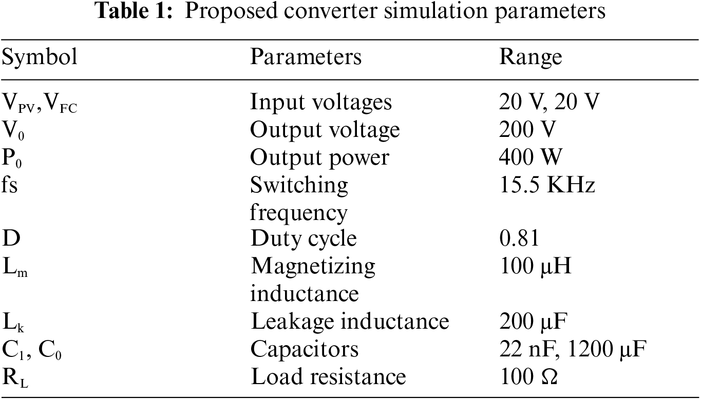
High power density, high reliability, act, and high-temperature recycling are the lithium-ion batteries characteristics. Be that as its one of demerits is the high cost [42]. Li-ion type batteries are utilized broadly due to their great act in practical electronic devices [43]. The proposed converter simulation parameters are appropriate in Tab. 1.
In order to fulfill the control battery state of charge (SOC), the ANFIS control mechanism is used. Here the battery to charger and discharge on their SOC, the ANFIS controller has a greater dynamic response, and it has the merits of less stable errors and faster response times. Comparative analysis has also been performed for better analysis of results; the results of the simulations confirm the newly implemented converter performance (Figs. 10 and 11) and show the transient behavior. Fig. 12 appears the output current and voltage waveform obtained from the proposed converter simulation. The system's output voltage remains very well regulated at the required level, with no overshoots. The output voltage of the system has a very low level of ripple Fig. 13.

Figure 10: Simulation results of input voltages and output voltage

Figure 11: Simulation result of the inductor current

Figure 12: Simulation results of load current and voltage

Figure 13: Simulation results of battery SOC, battery current, and voltage
Moreover, the MOSFET voltage stress is lower than the output voltage. As a result of soft switching technology, turn-OFF switching losses in each switch would be reduced and helps to improve the system efficiency.
From Fig. 14, the normalized voltage stress with respect to the semiconductor is significantly less than with other converters. Inductor current sharing is obviously greater, which reduces the current ripple.

Figure 14: Switch voltage stress vs. duty cycle
This reduces the output capacitor's size and increases the converter's overall power density. Fig. 15 shows the converter efficiency. Subsequently, the proposed converter made it incredibly reasonable for connecting a renewable energy application that needed high voltage gain and efficiency. All of the simulation results show that the proposed interleaved non-isolated great boost dc-dc converter control technique for renewable energy system applications will provide reasonable results even when converter operations change.

Figure 15: Output power and efficiency
The following discussion points may be extracted from the simulations and case studies mentioned above.
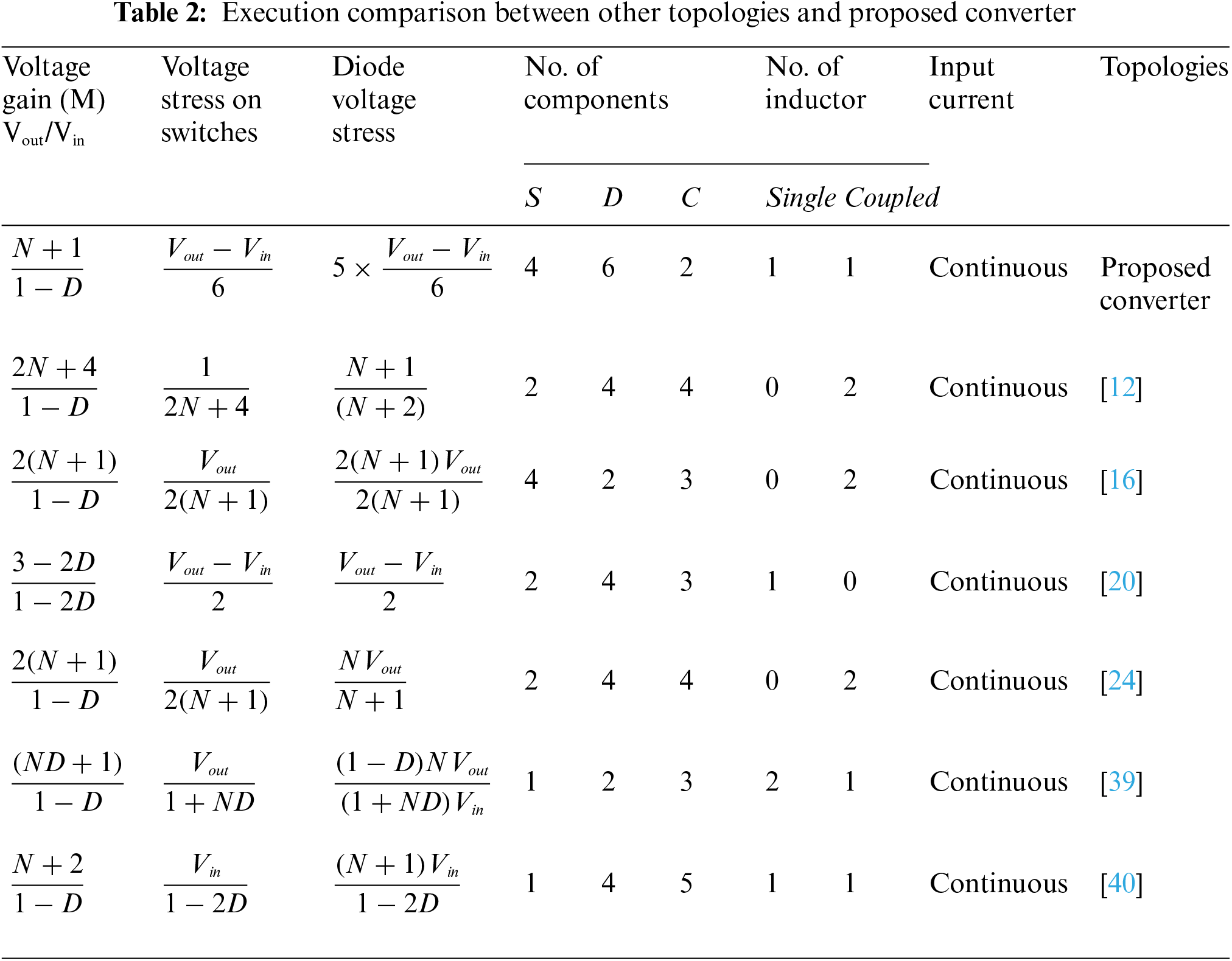
–An impartiality comparison with previous research validates the constructed interleaved non-isolated coupled inductor-based high step-up dc-dc converter, as shown in Tab. 2.
–The simulation results illustrate the transient behavior of the newly implemented converter Figs. 10 and 11. The output current and voltage waveforms from the suggested converter simulation are shown in Fig. 12.
–The ANFIS controller (Fig. 6) has a fast response time, a better dynamic response, and it is utilized to monitor the output voltage variations.
–Voltage stress with respect to the semiconductor The ANFIS controller (Fig. 14) is significantly less than with other converters, and efficiency also improved (Fig. 14).
–A non-isolated interleaved high gain DC-DC converter with coupled inductor was proposed and to attain a high gain of voltage.
A non-isolated interleaved high gain DC-DC converter with coupled inductor was proposed in this paper in order to attain a high gain of voltage without a high turn ratio. In the absence of one or two resources, the converter is capable of supplying the required power to the load. The modeled converter is in three separate operating states and is used to create a suitable controller. The gain of voltage, stress voltage on the switches and diodes, conduction losses, and performance of the proposed converter were all studied. The percentage of voltage stress on diodes and switches was lower in the proposed converter as compared to the output voltage, and low-voltage rated MOSFETs with a limited ON-resistance were supplied to minimize the loss of conduction. It is also possible to obtain a low-ripple continuous input current, and the ANFIS regulation technique would be used to monitor the output voltage variations. The converter process is evaluated and verified using Matlab/Simulink simulation.
Acknowledgement: This research was funded by the Deanship of Scientific Research at Princess Nourah bint Abdulrahman University through the Fast-track Research Funding Program.
Funding Statement: This research was funded by the Deanship of Scientific Research at Princess Nourah bint Abdulrahman University through the Fast-track Research Funding Program.
Conflicts of Interest: The authors declare that they have no conflicts of interest to report regarding the present study.
1. N. Eghtedarpour and E. Farjah, “Distributed charge/discharge control of energy storages in a renewable-energy-based DC micro-grid,” IET Renewable Power Generation, vol. 8, no. 1, pp. 45–57, 2014. [Google Scholar]
2. R. Sedaghati and M. R. Shakarami, “A novel control strategy and power management of hybrid PV/FC/SC/battery renewable power system-based grid-connected microgrid,” Sustainable Cities and Society, vol. 44, pp. 830–843, 2019. [Google Scholar]
3. S. Moury, J. Lam, V. Srivastava and R. Church, “New soft-switched multi-input converters with integrated active power factor correction for hybrid renewable energy applications,” in IEEE Energy Conversion Congress and Exposition, ECCE 2016, Milwaukee, Wl, USA, pp. 1–8, 2016. [Google Scholar]
4. A. Kuriqi, A. N. Pinheiro, A. Sordo-Ward and L. Garrote, “Water-energy-ecosystem nexus: Balancing competing interests at a run-of-river hydropower plant coupling a hydrologic–ecohydraulic approach,” Energy Conversion and Management, vol. 223, pp. 1–19, 2020. [Google Scholar]
5. S. Sathyan, H. M. Suryawanshi, M. S. Ballal and A. B. Shitole, “Soft-switching DC-dC converter for distributed energy sources with high step-up voltage capability,” IEEE Transactions on Industrial Electronics, vol. 62, no. 11, pp. 7039–7050, 2015. [Google Scholar]
6. X. Wu, J. Zhang, X. Ye and Z. Qian, “Analysis and derivations for a family ZVS converter based on a new active clamp ZVS cell,” IEEE Transactions on Industrial Electronics, vol. 55, no. 2, pp. 773–781, 2008. [Google Scholar]
7. S. Gorjian, H. Sharon, H. Ebadi, K. Kant, F. Bontempo et al., “Recent technical advancements economics and environmental impacts of floating photovoltaic solar energy conversion systems,” Journal of Cleaner Production, vol. 278, pp. 1–28, 2021. [Google Scholar]
8. M. Kumar, S. S. Chandel and A. Kumar, “Performance analysis of a 10 MWp utility scale grid-connected canal- top photovoltaic power plant under Indian climatic conditions,” Energy, vol. 204, pp. 1–14, 2020. [Google Scholar]
9. A. Alhejji, A. Kuriqi, J. Jurasz and F. K. Abo-Elyousr, “Energy harvesting and water saving in arid regions via solar pv accommodation in irrigation canals,” Energies, vol. 14, no. 9, pp. 1–25, 2021. [Google Scholar]
10. A. Rajaei, R. Khazan, M. Mahmoudian, M. Mardaneh and M. Gitizadeh, “A dual inductor high step-up DC-DC converter based on the cockcroft-walton multiplier,” IEEE Transactions on Power Electronics, vol. 33, no. 11, pp. 9699–9709, 2018. [Google Scholar]
11. S. Sathyan, H. M. Suryawanshi, B. Singh, C. Chakraborty, V. Verma et al., “ZVS–ZCS high voltage gain integrated boost converter for DC microgrid,” IEEE Transactions on Industrial Electronics, vol. 63, no. 11, pp. 6898–6908, 2016. [Google Scholar]
12. Y. Zheng and K. M. Smedley, “Interleaved high step-up converter integrating coupled inductor and switched capacitor for distributed generation systems,” IEEE Transactions on Power Electronics, vol. 34, no. 8, pp. 7617–7628, 2019. [Google Scholar]
13. P. Kong and G. K. Karagiannidis, “Charging schemes for plug-in hybrid electric vehicles in smart grid: A survey,” IEEE Access, vol. 4, pp. 6846–6875, 2016. [Google Scholar]
14. M. A. Abusara, J. M. Guerrero and S. M. Sharkh, “Line-interactive UPS for microgrids,” IEEE Transactions on Industrial Electronics, vol. 61, no. 3, pp. 1292–1300, 2013. [Google Scholar]
15. A. Naderi and K. Abbaszadeh, “High step-up DC-DC converter with input current ripple cancellation,” IET Power Electron, vol. 9, no. 12, pp. 2394–2403, 2016. [Google Scholar]
16. M. Forouzesh, Y. Shen, K. Yari, Y. P. Siwakoti and F. Blaabjerg, “High-efficiency high step-up DC-DC converter with dual coupled inductors for grid-connected photovoltaic systems,” IEEE Transactions on Power Electronics, vol. 33, no. 7, pp. 5967–5982, 2017. [Google Scholar]
17. S. M. Chen, M. L. Lao, Y. H. Hsieh, T. J. Liang and K. H. Chen, “A novel switched-coupled-inductor DC-DC step-up converter and its derivatives,” IEEE Transactions on Industry Applications, vol. 51, no. 1, pp. 309–314, 2014. [Google Scholar]
18. T. Kerekes, R. Teodorescu and U. Borup, “Transformerless photovoltaic inverters connected to the grid,” in Twenty-Second Annual IEEE Applied Power Electronics Conf. and Exposition, APEC 07, Anaheim, CA,USA, pp. 1733–1737, 2007. [Google Scholar]
19. M. L. Alghaythi, R. M. O'connell and N. E. Islam, “Design of a high step-up DC-DC power converter with voltage multiplier cells and reduced losses on semiconductors for photovoltaic systems,” in 2019 IEEE Electrc Ship Technologies Symp. (ESTSWashington, DC, USA, pp. 214–218, 2019. [Google Scholar]
20. M. Nguyen, T. Duong and Y. Lim, “Switched-capacitor based dual-switch high-boost DC-DC converter,” IEEE Transactions on Power Electronics, vol. 33, no. 5, pp. 4181–4189, 2018. [Google Scholar]
21. Y. Sato, M. Uno and H. Nagata, “Non-isolated multiport converters based on integration of PWM converter and phase-shift-switched capacitor converter,” IEEE Transactions on Power Electronics, vol. 35, no. 1, pp. 455–470, 2020. [Google Scholar]
22. L. H. S. C. Barreto, E. A. A. Coelho, V. J. Farias, J. C. de Oliveira, L. C. de Freitas et al., “A quasi-resonant quadratic boost converter using a single resonant network,” IEEE Transactions on Industrial Electronics, vol. 52, no. 2, pp. 552–557, 2005. [Google Scholar]
23. B. Singh, V. Bist, A. Chandra and K. A. Haddad, “Power factor correction in bridgeless-luo converter fed BLDC motor drive,” IEEE Transactions on Industry Applications, vol. 51, no. 2, pp. 1179–1188, 2015. [Google Scholar]
24. Y. Zhang, Y. Gao, L. Zhou and M. Sumner, “A switched-capacitor bidirectional DC-DC converter with wide voltage gain range for electric vehicles with hybrid energy sources,” IEEE Transactions on Power Electronics, vol. 33, no. 11, pp. 9459–9469, 2018. [Google Scholar]
25. F. Radmand and A. Jalili, “A novel switched-capacitor based high step-up DC-DC converter for renewable energy system applications,” Journal of Power Electronics, vol. 17, no. 6, pp. 1402–1412, 2017. [Google Scholar]
26. M. Forouzesh, Y. P. Siwakoti, S. A. Gorji, F. Blaabjerg and B. Lehman, “Step-up DC-DC converters: A comprehensive review of voltage-boosting techniques, topologies, and applications,” IEEE Transactions on Power Electronics, vol. 32, no. 12, pp. 9143–9178, 2017. [Google Scholar]
27. S. Kumaravel, R. A. Narayanankutty, V. S. Rao and A. Sankar, “Dual input-dual output DC-DC converter for solar PV/battery/ultra-capacitor powered electric vehicle application,” IET Power Electronics, vol. 12, no. 13, pp. 3351–3358, 2019. [Google Scholar]
28. F. Akar, Y. Tavlasoglu, E. Ugur, B. Vural and I. Aksoy, “A bidirectional non-isolated multi-input DC-dC converter for hybrid energy storage systems in electric vehicles,” IEEE Transactions on Vehicular Technology, vol. 65, no. 10, pp. 7944–7955, 2015. [Google Scholar]
29. L. Yu and H. Wang, “A novel dual-input ZVS DC-DC converter for low-power energy harvesting applications,” IEEE Journal of Emerging and Selected Topoics in Power Electronics, vol. 7, no. 2, pp. 1197–1206, 2018. [Google Scholar]
30. Y. Huang, S. C. Tan and S. Y. Hui, “Multiphase-interleaved high step-up DC-DC resonant converter for wide load range,” IEEE Transactions on Power Electronics, vol. 34, no. 8, pp. 7703–7718, 2018. [Google Scholar]
31. R. R. Ahrabi, H. Ardi, M. Elmi and A. Ajami, “A novel step-up multiinput DC-DC converter for hybrid electric vehicles application,” IEEE Transactions on Power Electronics, vol. 32, no. 5, pp. 3549–3561, 2016. [Google Scholar]
32. S. Sathyan, H. M. Suryawanshi and A. B. Shitole, “Soft switched coupled inductor based high step up converter for distributed energy resources,” in IECON 2014–40th Annual Conf. of the IEEE Industrial Electronics Society, Dallas, TX, USA, pp. 1799–1805, 2014. [Google Scholar]
33. K. Park, G. Moon and M. Youn, “Non-isolated high step-up boost converter integrated with sepic converter,” IEEE Transactions on Power Electronics, vol. 25, no. 9, pp. 2266–2275, 2010. [Google Scholar]
34. S. Dwari and L. Parsa, “An efficient high-step-up interleaved DC-DC converter with a common active clamp,” IEEE Transactions on Power Electronics, vol. 26, no. 1, pp. 66–78, 2010. [Google Scholar]
35. M. Premkumar, C. Kumar and R. Sowmya, “Analysis and implementation of high-performance DC-dC step-up converter for multilevel boost structure,” Frontiers in Energy Research, vol. 7, no. 149, pp. 1–11, 2019. [Google Scholar]
36. Y. P. Siwakoti and F. Blaabjerg, “Single switch non-isolated ultra-step-up DC-DC converter with an integrated coupled inductor for high boost applications,” IEEE Transactions on Power Electronics, vol. 32, no. 11, pp. 8544–8558, 2017. [Google Scholar]
37. V. J. Samuel, G. Keerthi and P. Mahalingam, “Coupled inductor-based DC-dC converter with high voltage conversion ratio and smooth input current,” IET Power Electronics, vol. 13, no. 4, pp. 733–743, 2020. [Google Scholar]
38. A. Kumar and P. Sensarma, “Ripple-free input current high voltage gain DC-DC converters with coupled inductors,” IEEE Transactions on Power Electronics, vol. 34, no. 4, pp. 3418–3428, 2019. [Google Scholar]
39. W. Hassan, D. D. C. Lu and W. Xiao, “Analysis and experimental verification of a single-switch high-voltage gain ZCS DC–DC converter,” IET Power Electronics, vol. 12, no. 8, pp. 2146–2153, 2019. [Google Scholar]
40. A. Khaligh and Z. Li, “Battery, ultracapacitor, fuel cell, and hybrid energy storage systems for electric, hybrid electric, fuel cell, and plug-in hybrid electric vehicles: State of the art,” IEEE Transaction on Vehicular Technology, vol. 59, no. 6, pp. 2806–2814, 2010. [Google Scholar]
41. A. A. Aldair, A. A. Obed and A. F. Halihal, “Design and implementation of ANFIS-reference model controller based MPPT using FPGA for photovoltaic system,” Renewable and Sustainable Energy Reviews, vol. 82, no. part 3, pp. 2202–2217, 2018. [Google Scholar]
42. G. J. Osório, J. C. O. Matias and J. P. S. Catalão, “Short-term wind power forecasting using adaptive neuro-fuzzy inference system combined with evolutionary particle swarm optimization, wavelet transform and mutual information,” Renewable Energy, vol. 75, pp. 301–307, 2015. [Google Scholar]
43. P. García, C. A. García, L. M. Fernández, F. Llorens and F. Jurado, “ANFIS-Based control of a grid-connected hybrid system integrating renewable energies, hydrogen and batteries,” IEEE Transactions on Industrial Informatics, vol. 10, no. 2, pp. 1107–1117, 2014. [Google Scholar]
 | This work is licensed under a Creative Commons Attribution 4.0 International License, which permits unrestricted use, distribution, and reproduction in any medium, provided the original work is properly cited. |