DOI:10.32604/cmc.2022.022027
| Computers, Materials & Continua DOI:10.32604/cmc.2022.022027 | |
| Article |
Computational Investigation of Multiband EMNZ Metamaterial Absorber for Terahertz Applications
1Space Science Center, Universiti Kebangsaan Malaysia, 43600, UKM Bangi, Selangor, Malaysia
2Department of Computer and Communication Engineering, Faculty of Computer Science and Engineering, Patuakhali Science and Technology University, Bangladesh
3Department of Electrical, Electronic and Systems Engineering, Faculty of Engineering and Built Environment, Universiti Kebangsaan Malaysia, Malaysia
*Corresponding Author: Mohd Hafiz Baharuddin. Email: hafizb@ukm.edu.my
Received: 25 July 2021; Accepted: 22 September 2021
Abstract: This study presents an Epsilon Mu near-zero (EMNZ) nanostructured metamaterial absorber (NMMA) for visible regime applications. The resonator and dielectric layers are made of tungsten (W) and quartz (fused), where the working band is expanded by changing the resonator layer's design. Due to perfect impedance matching with plasmonic resonance characteristics, the proposed NMMA structure is achieved an excellent absorption of 99.99% at 571 THz, 99.50% at 488.26 THz, and 99.32% at 598 THz frequencies. The absorption mechanism is demonstrated by the theory of impedance, electric field, and power loss density distributions, respectively. The geometric parameters are explored and analyzed to show the structure's performance, and a near-field pattern is used to explain the absorption mechanism at the resonance frequency point. The numerical analysis method describes that the proposed structure exhibited more than 80% absorbability between 550 and 900 THz. The Computer Simulation Technology (CST Microwave Studio 2019) software is used to design the proposed structure. Furthermore, CST-HFSS interference is validated by the simulation data with the help of the finite element method (FEM). The proposed NMMA structure is also exhibits glucose concentration sensing capability as applications. So the proposed broadband absorber may have a potential application in THz sensing, imaging (MRI, thermal, color), solar energy harvesting, light modulators, and optoelectronic devices.
Keywords: Metamaterial absorber; terahertz applications; multiband; EM near zero; nanostructured; visible regime applications
Metamaterials have entered the modern particularly dominant electromagnetism, high-frequency engineering, and materials science research inside a comparatively short period. It has overseen to discover a particular profile and visibility inside the preceding decade of the 21st century. In recent years, metamaterials have attained incredible consideration by researchers because of their exceptional electromagnetic properties spreading over the entire optical range extend that caused different types of technological application [1–3]. In surrounding air capable of instantaneously exciting electric and magnetic resonance to realize an impedance match, a perfect metamaterial absorber (PMA) was introduced in 2008 by [4].
Consequently, several metamaterial absorbers (MMA) designs with perfect impedances matched are explored during a wide frequency region, starting from microwaves to optical waves [5–8]. However, these perfect absorbers frequently operate at limited frequencies but may not cover multiple practical applications with specific requirements for bandwidth. Based on perfect metamaterial absorber (MMA), the further application field is explored by researchers. By the composites of metal-insulator-metal (MIM), the metamaterial absorbers (MMA) are developed and compared to convenient composites (metal-insulator-metal) performance. Different metamaterial has a significant to harvesting solar energy in THz ranges. As an example, Gold (Au) and silicon dioxide (SiO2) are used as a resonator and substrate, respectively [9]. A tri-layer (Ni-GaAs) split hexagonal shape MTM is designed with DNG characteristics for solar energy harvesting in a visible regime [10]. For a substantial variation of the nanoscale metamaterial absorber operating frequency range, the wavelength in free space should remain higher than unit cells [11]. A narrow band MTM absorber is designed and investigated based on a single windmill-shaped structure; then, the theory of multiple reflection interference is used analysis the absorption mechanism that exhibits polarization angle independently [12]. According to the concept of the sensing phenomena, a cylindrical metal structure is chosen [13] that exhibits the polarization independence and sensing capabilities in terahertz frequency ranges where the magnetic resonance is employed to analyze the sensing functionality of the structures. Another four layers (Silica, titanium, magnesium fluoride, and aluminum) ultra-wideband (UWB) absorber is designed and numerically investigated [14] that is exhibited up to 90% absorbability in the visible and near infrared region. This particular characteristic enables metamaterials to be used as antennas [15], waveguides [16], invisibility cloaking [17], absorbers [18,19], and various kinds of sensors [20]. Thermal stability has significance in achieving solar power conversion efficiency and perfect absorbability [21,22]. An ideal solar absorber must have the capability to convert most solar radiation into heat in the visible, infrared, and near-infrared areas [23].
This study presents a nanostructure metamaterial absorber to harvesting solar energy at the visible ranges. From the observation of literature reviews, broadband is not easily obtainable in optical regions. In this research article, tungsten and quartz (fused) have been used to modify the anticipated design to resist high temperatures and coordinated impedance with free space. In addition, quartz (fused) is exhibited minimal comparative permittivity inside the optical ranges and an extraordinary softening stage. The proposed structure is demonstrated an average absorption of up to 80% between 550–900 THz frequency spectrums with a peak absorption of 99.99%. The most effective absorption mechanism changes the shape by regulating the unit cell parameters and optimizing the dielectric layer. The geometrical structure produces plasmonic reverberation characteristics, and a metal ground plane can reduce reflection and transmission to maximize absorption. The optimization of the dielectric layer and parametric scan is used to validate the performance of the structure. The finite integration technique (FIT) and finite element method (FEM) are used in CST software to analyze the proposed structure. Moreover, CST-HFSS interference is used to validate the proposed structure's performance in the result and discussion section. OriginPro 2018 software is used in this study commercially available in the market for data extracting. Specific application of the terahertz (THz) absorber depends on its materials, and this material is used to block the energy of an incident particle. Various materials (lead, tungsten, and liquid hydrogen) are used to make different absorber types depending on their purpose of use [24]. The proposed EMNZ metamaterial design is appropriate for substantial absorption, wide-angle stability. This characteristic enables metamaterials as antennas, waveguides, and absorbers. Moreover, terahertz (THz) absorber also can be used as sensing, invisibility cloaking, magnetic resonance imaging (MRI), thermal imaging, and color images applications.
2 Methodology of the Multiband Nano-Meta
The proposed nanostructured metamaterial absorber (NMMA) consists of three layers (metal-dielectric-metal). The resonator and back-layer consist of tungsten (W), where quartz (fused) is used as the dielectric layer. The dielectric layer is a sandwich between the resonator and back-layer, with a dielectric constant (εr) of 3.8 and loss tangent (δ) of 0.0004. The tungsten (W) is chosen as a resonator layer because it has a high impedance matching capability that reduces reflection and transmission. Lossless and resonance characteristics of quartz (fused) support the design by perfectly impedance matching in the free space. This dielectric layer is used to produce capacitance and inductance with the help of a resonator, and the back layer occurs with high absorbability. In addition, tungsten (W) exhibits high-temperature stability (3422°C) and arbitrary absorptivity inside the optical region with a low ohmic loss. Quartz (fused) also has a very high melting point (1715°C) that helps the proposed structure achieve high absorption with wide bandwidth.
2.2 Geometric Layout of the Nano-Meta Unit Cell Structure
The proposed unit cell is consists of a resonator layer, dielectric layer, and back layer. The resonator layer is combined with three “T” like shapes, one “I” like shape, and the outer side has a split square ring resonator (SSRR) demonstrated in Fig. 1a. The resonator and unit cells’ back layers consist of tungsten (W) thicknesses of 20 and 120 nm, respectively. The dielectric layer is consists of quartz (fused) with a thickness of 50 nm, dielectric constant (εr) of 3.8, and loss tangent (δ) of 0.0004. The proposed nanostructure MMA is compact with its dimension (900 × 900 × 190 nm3) and total thickness (190 nm) of this structure is higher than the skin depth, skin depth, (δ) = (2ρ/2πfμRμ0)1/2 that's why this structure is called as a meta-atom. The geometric parameters of the unit cell are listed in Tab. 1. This dielectric layer is a continuous board that is accustomed to blocking the transmission of incident electromagnetic waves. The proposed structure dielectric layer is a sandwich between the resonator and back-layer, shown in Fig. 1b.

Figure 1: Schematic diagram of the proposed NMMA structure (a) front view and (b) side view

The perfect electric conductor (PEC) and the perfect magnetic conductor (PMC) are used to arranging an ideal environment, shown in Fig. 2. This design simplest emphasizes that transverse electromagnetic waves (TEM) and Z-axis are considered open areas in which frequencies pass over the structure. Thus, propagation direction followed electric and magnetic fields X, Y, and Z axes, severally. The Incident electromagnetic field is applied generally to the resonator on Z-axis. A semiconductor material is used in a photovoltaic (PV) solar system, whose sunlight hits a solar panel. Then electron motion occurs, and this electron motion creates an electric current that can be captured by wire. The sun electromagnetic radiation emitted area is a visible light regime in the frequency spectrum, so the proposed structure operates in the visible light region 550–900 THz. Frequency-domain solver microwave studio CST 2019 is used to design and simulate the proposed structure. The finite integration technique (FIT) and finite element method (FEM) are used in CST software to analyze the unit cell performance. In addition, parametric scans and optimization are used to validate the structure's performance. Moreover, CST and HFSS software is used to validate the structure. Finally, OriginPro 2018 software is performed for data extraction, which is commercially available in the market.

Figure 2: Boundary conditions of the proposed unit cell
2.3 Simulation Setup of Nano-Meta
The computer simulation technology (CST) software is used to continue the simulation, result, and discussion session. The perfect electric conductor (PEC) and perfect magnetic conductor (PMC) boundaries are applied in the Y and Z axis, respectively, shown in Fig. 2. The boundary condition is adequate to block close field inconvenience. This design simplest emphasizes that transverse electromagnetic waves (TEM) and Z-axis are considered an open area in which frequencies will pass over the structure. Propagation direction followed electric and magnetic fields X, Y, and Z axes, severally. The electric fields, magnetic fields, and open spaces are opposite to one another. Both structures are placed between positive and negative Z-axis waveguide ports to excite the resonating structure. The scattering parameter in both ports becomes available for further reflection analysis and characterization during the electromagnetic wave propagation. The finite integration technique (FIT) and the finite element method (FEM) are performed for CST software data analysis. Moreover, data analysis through the CST and HFSS is validated in the results and discussion section.
2.4 MMA Unit Cell Design Evaluation
The proposed EMNZ metamaterial unit cell consists of a resonator, dielectric, and back layer. The resonator of the proposed structure is compact with a split square ring resonator (SSRR), three T-like shapes, and one I-like shape. This study discusses the design evaluation of the proposed EMNZ unit cell. Figs. 3a–3c represent the design evaluation, significant effect of the transmission coefficient (S21), and absorbance of the unit cell. In step 1, with only a square ring resonator (SRR), this structure has a maximum magnitude of −19 and −14 dB between 585.43–601.55 THz and 685.4–727.65 THz, respectively. Maximum absorbance is achieved at 98.64%, 98.41%, and 97.02% at the frequency of 522.25, 622.85, and 716.50 THz, shown in Figs. 3a and 3b. At the top and bottom portion of the square ring resonator has cut a slot in steps 2, this structure has a maximum magnitude of −32.21, −22.32, and −17.95 dB in between the frequency of 618.14–648.79 THz, 714.14–768.80 THz, 808.78–836.79 THz, respectively. Three peak absorptions is achieved in these steps 99.70%, 99.60%, 99.37%, at the frequency of 600.68, 614.45, 705.83 THz, respectively. In step 3, we added two horizontal bars and two vertical bars inside the square split ring resonator (SSRR), increasing the bandwidth and average absorbance. In this step, this structure is achieved wide bandwidth than step 1 and step 2 in between 559.49–615.43 THz, 708.08–738.80 THz, and 786.49–816.05 THz but dramatically decreased the magnitude in this frequency range. Moreover, the proposed structure has achieved a maximum magnitude of −24 dB and absorption of 99.12% at a frequency of 722.76 THz. It stays up to 80% absorbability at the operating frequency spectrum. Meanwhile, at the right middle center and left edge corner again cut two slots; as a result, this step 4 is achieved more bandwidth in between 564.84–584.15 THz, 595.48–630.75 THz, 686.77–746.78 THz, 800.09–862.09 THz, and 879.411–982.73 THz. Moreover, at the frequency of 614.79 THz, this structure is achieved a maximum magnitude and absorption of −39.56 dB and 99.72%, respectively. Finally, we added three horizontal and vertical bars that make three T-like shapes and one I-like shape. Therefore, this proposed structure is increased its bandwidth and absorption. The numerical analysis method describes that the proposed design exhibited more than 80% absorbability between 550 and 900 THz. Due to perfect impedance matching with plasmonic resonance, a characteristic, the proposed structure is achieved an excellent absorption of 99.99% at 571 THz, 99.50% at 488.26 THz, 99.32% at 598 THz frequencies.

Figure 3: (a) Design evaluation (b) reflection coefficient (S21) and (c) absorbance
2.5 Geometric Parameter Sweep of the MMA Unit Cell
The absorption characteristic of the proposed unit cell structure is further studied in this section by sweeping some significant parameters to determine the perfect absorption. The effect of the structural parameters sweep is shown in Figs. 4a–4d, respectively. Tuning the unit cell width (W) between 880–920 nm with a step size of 10 nm, a significant variation of the absorption is observed in resonance frequency. The increment of width (W) linearly altered the resonance frequency of the structure 625.35, 630.30, 635.40, and 640.42 THz, respectively, with peak absorption values of 98.95%, 99.90%, 99.99%, 99.96%, and 99.95%, respectively, shows in Fig. 4a. After that varying, the split square ring resonator (SSRR) width (D) between 30–70 nm with a step size of 10 nm, the effect of the absorption curve is shown in Fig. 4b. At D = 50 nm proposed structure is achieved 99.97% at the frequency of 627.55 THz. Thus, the proposed NMMA is exhibited up to 80% absorbability in the entire operating frequency spectrum. However, a slight up-down is observed at the absorption curve when changing the L1 parameter value between 130–170 nm demonstrated in Fig. 4c. As a result, the resonance frequency is slightly moved, but peak absorption remains 99.99% at the resonance frequency. Another significant parameter (L2) also altered from 30–70 nm with a step size 10 nm during this parametric sweep proposed unit cell is exhibited 99.97% absorbability at the frequency of 628.84 THz shown in Fig. 4c. The variation of the L2 parameter causes increasing or decreasing capacitance value that affects the resonance frequency of the proposed unit cell and shifts toward the lower to the upper-frequency ran. This is because electromagnetic waves expose the structure that makes capacitance between the metallic and dielectric layers. As a result, a series capacitance is induced between the resonating layer and the back layer. Moreover, the capacitance value between the resonating and back layer is inversely proportional to the dielectric layer thickness (TD). So, the distance between the two layers is increased that effectively reduces the magnetic resonance.
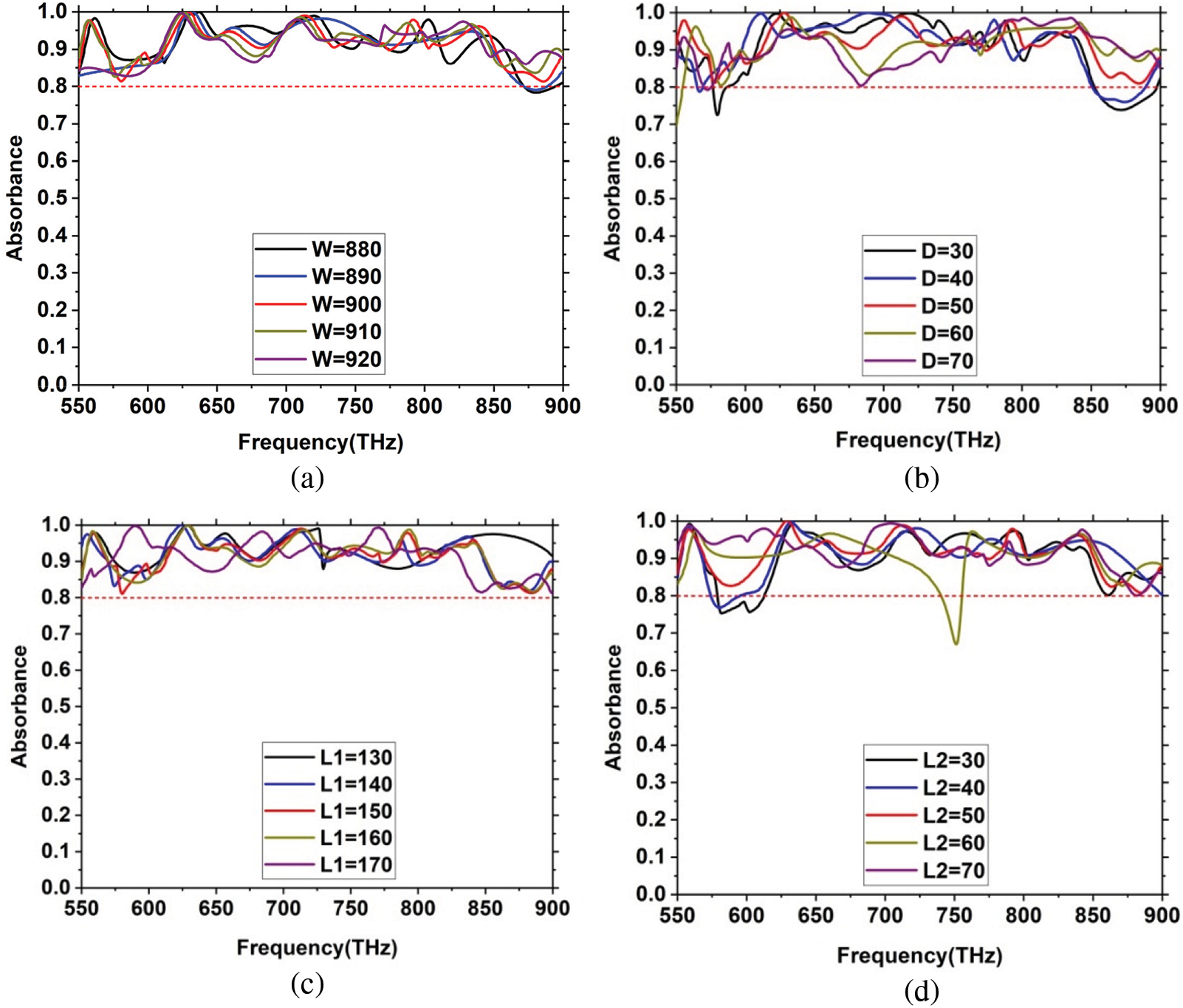
Figure 4: Parametric study of the structure (a) length of square shape structure “W” (b) width of SSRR “D” (c) length of the T shaped head “L1” (d) width of the T shape head “L2”
Moreover, these phenomena also decrease the capacitance value and absorbability of the proposed structure. When the dielectric layer thickness is altered 30–70 nm, the resonance frequency is linearly moved left to right, and the most relevant result is found at the thickness of TD = 50 nm. The resonance frequency is also increased with the decrease of its capacitance value; hence, the dielectric layer restricts most of the incident wave. This dielectric layer is also carried out as a highly acquired structure for perfect absorption. The following equation can calculate the absorption of any unit cell, A = 1-(R), since the dielectric layer thickness is enough to block the transmission (near zero). Lastly, the resonator layer thickness (TR) is also altered from 10–30 nm with a step size of 5 nm. Since the resonator thickness increases, the resonance frequency of the structure is also increased; tungsten (W) based resonator has tended toward lower frequency absorption. The thickness of the resonator layer is also proportional to the inductance and capacitance created by the structure. Therefore, this layer is formed an equivalent capacitance by increasing its thickness. The proposed NMMA has exhibited a maximum absorption of 99.99% at the thickness of 20 nm of the resonator layer. The perfect parameter's value is listed in Tab. 1.
3.1 Analysis of Effective Parameters
The proposed NMMA absorber is developed to harvest solar energy. Therefore, the compatibility of metamaterials has significance on the parameter performance. This structure selects tungsten (W) and quartz (fused) for optical, electrical, and scattering properties; it has a significant advantage on impedance matching [25]. Moreover, Tungsten (W) possesses high electrical conductivity, which enhances electron mobility. The quartz molecule (merged) used in this simulation has characteristics of the 4th-order dispersive models for satisfactory impedance matching the optical regime and free space [26]. The resonator layer consists of 20 nm thickness of the tungsten (W), shows in Fig. 1b. The dielectric layer quartz (fused) having a dielectric constant (εr), loss tangent (δ) of 3.8 and 0.0004, respectively, in the visible spectrum. Subsequently, the skin depth (δ) of the proposed NMMA is inversely proportional to the frequency. Therefore, it has a vital role in modifying the negative dielectric properties and the refractive index. The ground layer is made of quartz (fused), resistant to oxidation and corrosion, and not reactive with air. This substrate contains perfect conductivity and less resistivity to guide dynamic electrons for better mobility after photon conversion. In addition, the coupling capacitance between metallic and dielectric layers has improved the absorption characteristics of the proposed structure. Any material's dielectric property needs to be analyzed to verify the numerical analysis of absorption, photon conversion, and structural efficiency. The proposed absorber is characterized based on relative permittivity and relative permeability. This unit cell is achieved ENZ characteristics at the frequency of 552.4, 663.2, 728.8, and 862.8 THz, respectively. The relative permittivity value of the selected frequency point is 0.017, 0.012, 0.011, and 0.007, respectively, shown in Fig. 5c.
Along with sustainable development in theoretical research on photonics ENZ, many new functional photonic devices are proposed. Photonic epsilon near zero (ENZ) is the study of light interactions in the presence of structures with almost zero permittivity. The proposed structure is achieved near-zero relative permeability at the frequency of 58.2, 690.4, 774.4, and 801.22 THz, respectively. The relative permeability value at the selected frequency points is 0.0127, 0.014, 0.011, and 0.010, respectively, shown in Fig. 5d. The fractional absorption bandwidth and the characteristics of plasmonic resonance of the structure using the effective recovered impedance (Z) [11,27] are calculated by the following Eq. (1).
The surface conductivity of the structure is described by the following Kubo formula [28].
where air permittivity and vacuum permittivity are presented as σs and ε0, respectively. Angular frequency is represented by (ω), and the value of Δ is 50 nm.
The transmission line model of a structure shows that the real part of the impedance is near one, and the imaginary part is close to zero. Therefore, the real part of any transmission should be close to one, and the imaginary part approaches zero. Fig. 5a presents the reflection coefficient (S11) and transmission coefficient (S21) and absorption of the unit cell. Furthermore, two functions response (real and imaginary) is observed at normalized impedance (Z) curve, shows in Fig. 5b. Thus, the actual power receiving condition of the proposed NMMA unit cell with omnidirectional solar radiation has maximum absorption.
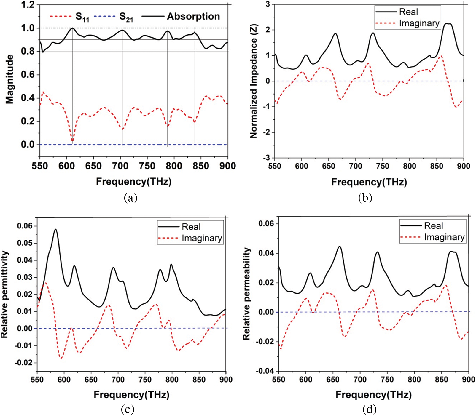
Figure 5: (a) Absorption (b) normalized impedance (c) relative permittivity and (d) relative permeability
3.2 Analysis of E-Field, H-Field and Surface Current Analysis
Proposed nanostructure metamaterial absorbers (NMMA) is exhibited perfect absorbability at the frequency of 532.65, 609.34, 702.38, and 786.15 THz, respectively. These selected frequency points represent the localized resonance of the structure. The electric field analyses the origin of these frequency points shown in Figs. 6a–6d, respectively. The electric field of the selected point is trapped in the tungsten resonators at the unit cell's boundaries. It is noticed that the trapped positions are different at different frequencies. For example, electric field |E| at 609.34 THz frequencies mostly captures short bar “I” like shape shown in Fig. 6b. On the other hand, 532.65 and 786.15 THz frequency is associated with the structure's excitation of square shape edge. Conversely, the electric field |E| at the frequency of 532.65, 609.34, and 786.15 THz is shown in Figs. 6a–6d are mainly gathered in the “T” like shape. Its means that the frequency of 532.65, 609.34, and 786.15 THz is linked to the “T” shape's localized resonances. Mostly observing that the electric field |E| at 702.38 and 786.15 THz are almost similar.
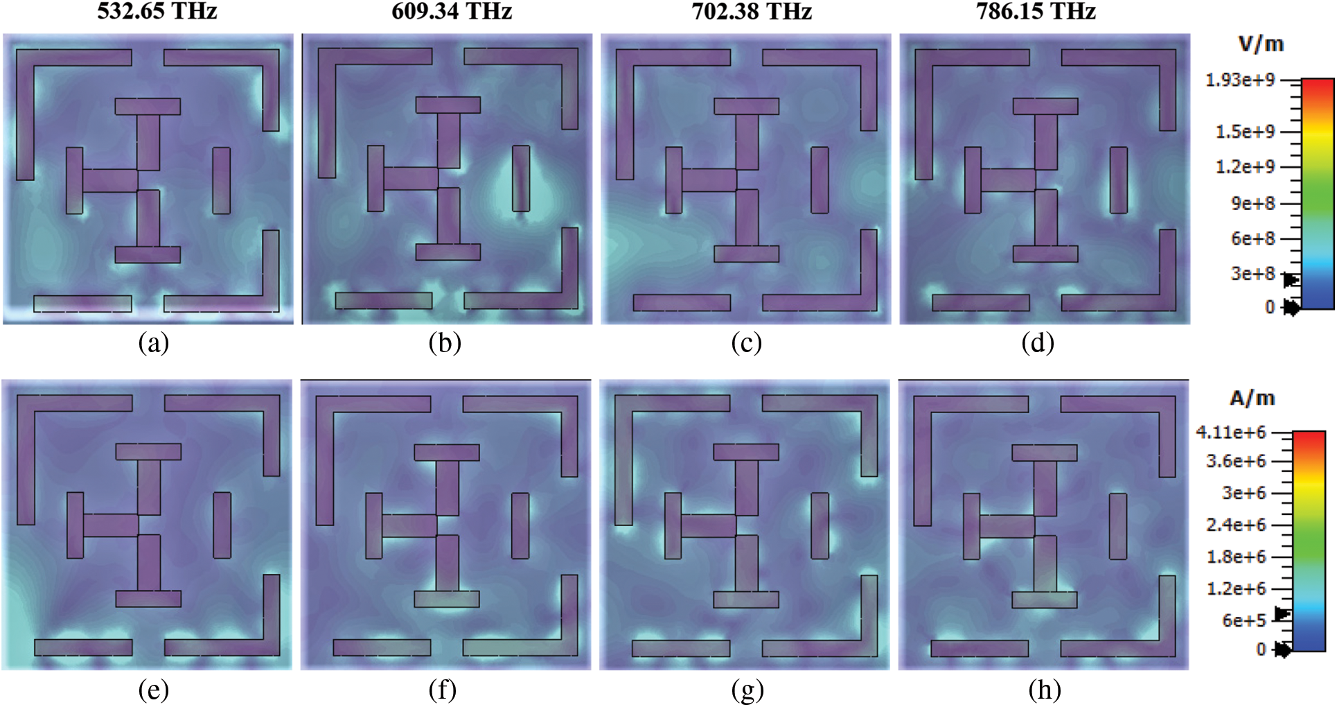
Figure 6: E field distribution is shown at (a) 532.65 THz (b) 609.34 THz (c) 609.34 THz (d) 786.15 TH, and H field distribution is shown at (e) 532.65 THz (f) 609.34 THz (g) 609.34 THz (h) 786.15 TH, respectively
Magnetic fields |Hy| of the proposed structure mainly focus on the resonator layer at 532.65, 609.34, 702.38, and 786.15 THz shows in Figs. 6e–6h,In Fig. 6 parts (a-h) are labeled but those parts should also be included in the figure legends. Please edit the legend to include those parts. respectively. The magnetic field |Hy| at the frequency of 532.65 THz is merely trapped with a single accumulation area at the lower portion of the structure resonator layer, shown in Fig. 6e. The magnetic field |Hy| mechanisms at the frequency of 609.34, 702.38, and 786.15 THz should be localized resonances of the structure's T shape. Since the magnetic field |Hy| of the structure is trapped, outer portions of the T-shaped shows in Figs. 6e–6h, respectively. At 532.65 and 702.38 THz, the operating mechanisms are different and originated from the particular localized resonator. The mechanisms at the frequency of 609.34 and 786.15 THz must be assigned to several coupling resonators from their magnetic field |Hy| are not merely trapped upper part of the SSRR resonator layer. The magnetic field created by dipole resonance coupled with incident electromagnetic field gives rise to a strong magnetic field.
The resonator layer surface current is analyses to understand the absorption mechanism of the structure. Rotary behavior (clockwise and anticlockwise) high current flow is observed at the back layer of the proposed unit cell shows in Figs. 7a–7d, respectively. A high-intensity electric current is kept at the lower portion of the split square ring resonator (SSRR) that substantially impacts the magnetic field. In the I-like shape, a random nature surface current and a more concentrated high current are observed at the frequency of 532.65 THz, as shown in Fig. 7a. At the frequency of 609.34 THz, a more directional current is observed lower portion and middle of the resonator layer shown in Fig. 7b. At the frequency of 702.38 THz, directional high current flows are observed on top of the split square ring resonator (SSRR) shown in Fig. 7c. In addition, an antiparallel current is kept at the frequency of 786.15 THz in oppositely placed two T-like-shape. Also, clockwise and anticlockwise current loops are observed in lower current loops and upper current loops, respectively, shown in Fig. 7d. The resonator and back layers work together to create magnetic resonance, mainly where observed antiparallel current between the resonator and back layer shown in Fig. 6e. This strong magnetic field interacts with the incident electromagnetic waves and helps obtain a high absorption level in the operating frequency spectrum. However, this current intensity is very low and has no significant effect on the magnetic field. In addition, an antiparallel current is observed between the front and back layers produce a strong magnetic field. This localized resonant magnetic field helps to obtain high absorption.
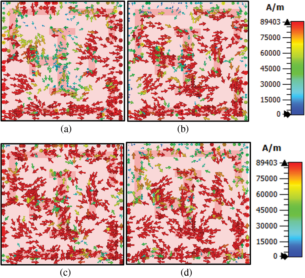
Figure 7: Surface current distributions at the frequency of (a) 532.65 THz (b) 609.34 THz (c) 702.38 THz (d) 786.15 THz
3.3 Demonstrates the Simulated Data with the Validation of CST and HFSS
Computer simulation technology CST STUDIO SUITE® 2019 and ANSYS HFSS 2018 simulation software design and demonstrate the proposed unit cell [29,30]. We have used to validate our work on two different methods based on computational software HFSS and CST. The finite integration technique (FIT) and finite element method (FEM) are used in CST and HFSS software to analyze unit cell performance. Figs. 8a and 8b demonstrate the absorption curve and reflection curve compared to the CST and HFSS software. The maximum magnitude of S11 parameters shows −36 and−38 dB, respectively CST and HFSS software. Thus, the maximum absorption stays nearly equal at 99.99%, and the average absorption is above 80% for both CST and HFSS in the whole frequency spectrum. Additionally, this study observes that the reflection coefficient (S11) parameter is synchronized perfectly, and it is the most significant phenomenon behind perfect absorption. However, in the reflection coefficient (S11) and absorption curve of Fig. 8, we observed a slight difference because of the different methods used in CST (Finite Integration Method) and HFSS (Finite Element Method) software. Moreover, a reference plane is used in CST software, but HFSS software didn't use any reference plane.
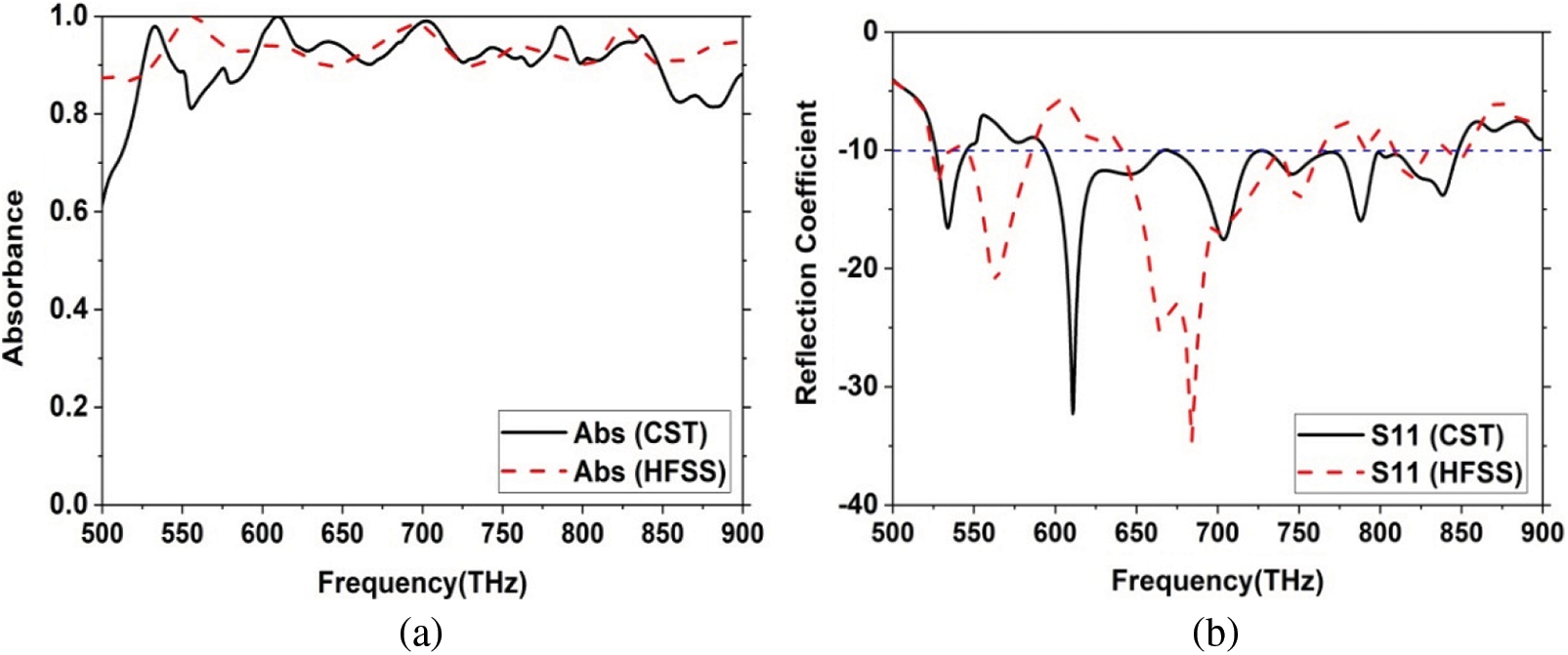
Figure 8: Validation of simulated results in between CST-HFSS software (a) absorption (b) reflection coefficient (S11)
3.4 Properties of the Glucose Concentration Detection of the Proposed NMMA Structure as Applications
This section presents the detection response of different glucose concentrations in the nanostructure metamaterial absorber (NMMA) water in the CST simulation environment. Above the dielectric layer, a surrounding environment of glucose sensing medium is shown in Fig. 9a. The response of the proposed NMMA is simulated for a different concentration between 0 g/100 ml to 50 g/100 ml. The refractive index (n) of the glucose concentration in water can be determined by using the refractometric method [31]. The following formula in Eq. (3) is used to calculate the refractive index (n) of glucose concentration.
Here,
Eq. (3) is used to determine the refractive index (RI) of glucose concentration in the range of 0–50 g in 100 ml of water. Then, the different IR (n1, n2, n3, n4, and n5) values were obtained for different water concentrations where the refractive index of water (
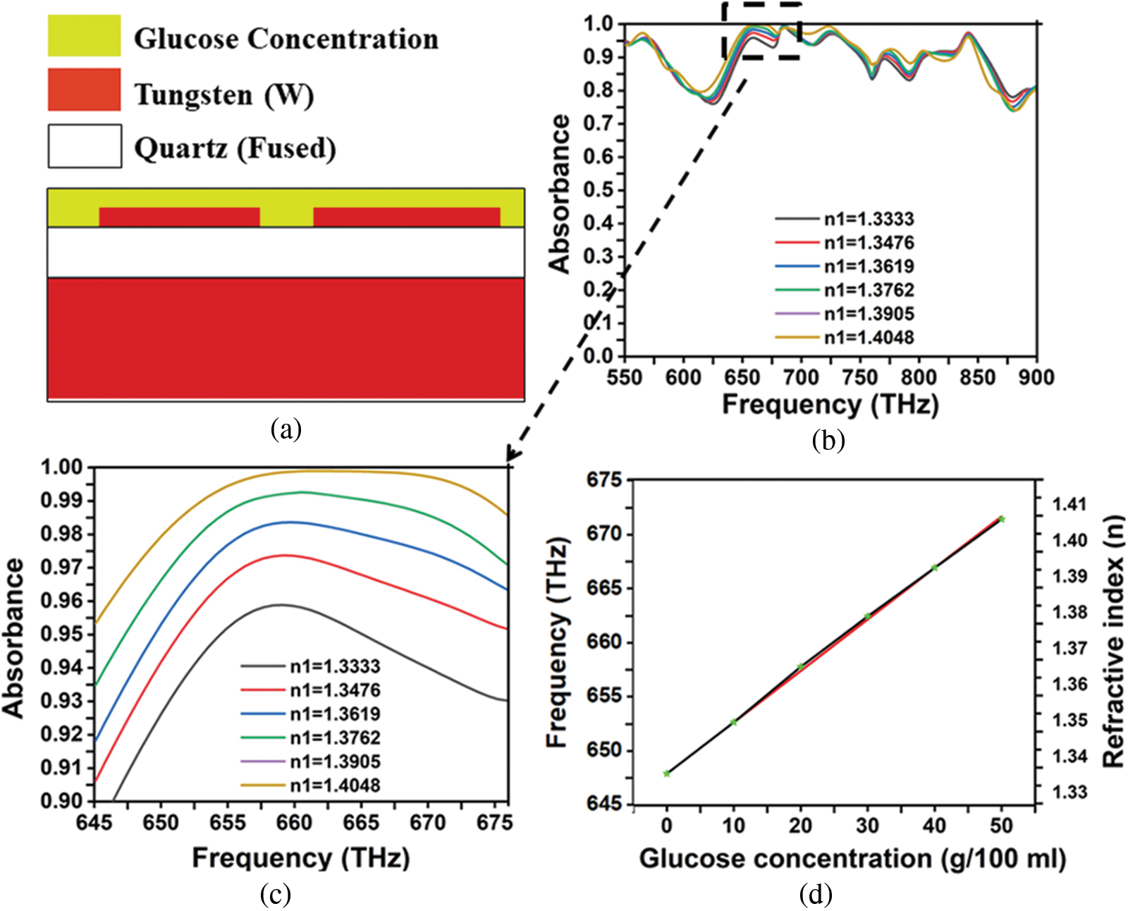
Figure 9: (a) Glucose concentration sensing medium, (b) absorption curve with different refractive index, (c) clear view of the selective peak absorption for sensing, (d) glucose concentration vs. refractive index (n) and frequency
The proposed design finds a substantial absorption compared to previous work, where Tab. 2 presents the performance of the proposed work and previous work. The proposed unit cell offers an average absorption of 80% and perfect absorption of 99.99%. The proposed distinctive geometric structure combines three T-like shapes, one I-like shape inside a split square ring resonator to improve absorption property. The exceptional softening level of tungsten and quartz (fused), effectiveness, and operating area differed from the materials is used in Tab. 2.

This paper presents an epsilon mu near-zero (EMNZ) nanostructure metamaterial absorber (NMMA) to apply a visible range. The resonator layer and dielectric layer are made of tungsten (W) and quartz (fused). The dielectric layer is a sandwich between the resonator layer and the back layer. This dielectric layer has a dielectric constant (εr), loss tangent (δ) of 3.8, and 0.0004. The proposed structure can be maintained with electromagnetic polarization. The proposed absorber provides more than 90% average absorption within bandwidth extended from 454.4–474.8 THz, 522–602.8 THz, 621.2–662.8 THz, and 694.4–784.4 THz. Thus, the maximum absorption is achieved by 99.8%, 99.9%, 99.92%, and 99.92% at the frequency of 465.2, 585.2, 648.8, and 762.8 THz. The proposed NMMA has been explored by studying the electric field and magnetic field at the resonance frequency absorption. This absorber can be used as an optical sensor to shift the resonance and changes in the dielectric layer and the resonator's thickness. The combustion points of material are applied to this study adds substantial absorbance related to broadband absorbers. The proposed structure is also exhibited glucose concentration sensing characteristics. In addition, the related analysis is conducted with peak absorption, absorption rate and the dimension of the structure, etc. The proposed broadband absorber may have a potential application in THz sensing, imaging (MRI, thermal, color), solar energy harvesting, light modulators, and optoelectronic devices. Compared to the previously published broadband absorbers, the proposed NMMA has the conventional improvement and efficiency of numerous possible applications in the optical frequency range.
Funding Statement: This work is supported by the Universiti Kebangsaan Malaysia research grant GGPM 2020-005.
Conflicts of Interest: The authors declare that they have no conflicts of interest to report regarding the present study.
1. N. Mou, X. Liu, T. Wei, H. Dong, Q. He et al., “Large-scale, low-cost, broadband and tunable perfect optical absorber based on phase-change material,” Nanoscale, vol. 12, pp. 5374–5379, 2020. [Google Scholar]
2. A. Alam, S. S. Islam, M. Islam, A. F. Almutairi and M. T. Islam, “Polarization-independent ultra-wideband metamaterial absorber for solar harvesting at infrared regime,” Materials, vol. 13, pp. 2560, 2020. [Google Scholar]
3. S. Mahmud, S. S. Islam, A. F. Almutairi and M. T. Islam, “A wide incident angle, ultrathin, polarization-insensitive metamaterial absorber for optical wavelength applications,” IEEE Access, vol. 8, pp. 129525–129541, 2020. [Google Scholar]
4. N. I. Landy, S. Sajuyigbe, J. J. Mock, D. R. Smith and W. J. Padilla, “Perfect metamaterial absorber,” Physical Review Letters, vol. 100, pp. 207402, 2008. [Google Scholar]
5. Y. Q. Ye, Y. Jin and S. He, “Omnidirectional, polarization-insensitive and broadband thin absorber in the terahertz regime,” JOSA B, vol. 27, pp. 498–504, 2010. [Google Scholar]
6. X. Liu, T. Starr, A. F. Starr and W. J. Padilla, “Infrared spatial and frequency selective metamaterial with near-unity absorbance,” Physical Review Letters, vol. 104, pp. 207403, 2010. [Google Scholar]
7. N. Thi Quynh Hoa, P. Huu Lam and P. Duy Tung, “Wide-angle and polarization-independent broadband microwave metamaterial absorber,” Microwave and Optical Technology Letters, vol. 59, pp. 1157–1161, 2017. [Google Scholar]
8. C. -H. Lin, R. -L. Chern and H. -Y. Lin, “Polarization-independent broadband nearly perfect absorbers in the visible regime,” Optics Express, vol. 19, pp. 415–424, 2011. [Google Scholar]
9. S. K. Patel, S. Charola, J. Parmar and M. Ladumor, “Broad-band metasurface solar absorber in the visible and near-infrared region,” Materials Research Express, vol. 6, pp. 086213, 2019. [Google Scholar]
10. A. Hoque, M. T. Islam, A. F. Almutairi and M. R. I. Faruque, “Design of split hexagonal patch array shaped nano-metaabsorber with ultra-wideband absorption for visible and uv spectrum application,” Nanoscale Research Letters, vol. 14, pp. 1–10, 2019. [Google Scholar]
11. D. Smith, D. Vier, T. Koschny and C. Soukoulis, “Electromagnetic parameter retrieval from inhomogeneous metamaterials,” Physical Review E, vol. 71, pp. 036617, 2005. [Google Scholar]
12. W. Pan, T. Shen, Y. Ma, Z. Zhang, H. Yang et al., “Dual-band and polarization-independent metamaterial terahertz narrowband absorber,” Applied Optics, vol. 60, pp. 2235–2241, 2021. [Google Scholar]
13. A. Elakkiya, S. Radha, B. Sreeja and E. Manikandan, “Terahertz metamaterial absorber with sensing capabilities,” Journal of Optoelectronics and Advanced Materials, vol. 22, pp. 360–364, 2020. [Google Scholar]
14. J. Liu, W. -Z. Ma, W. Chen, G. -X. Yu, Y. -S. Chen et al., “Numerical analysis of an ultra-wideband metamaterial absorber with high absorptivity from visible light to near-infrared,” Optics Express, vol. 28, pp. 23748–23760, 2020. [Google Scholar]
15. M. M. Hasan, M. R. I. Faruque and M. T. Islam, “Dual band metamaterial antenna for LTE/bluetooth/WiMAX system,” Scientific Reports, vol. 8, pp. 1–17, 2018. [Google Scholar]
16. F. Fan, X. Zhang, S. Li, D. Deng, N. Wang et al., “Terahertz transmission and sensing properties of microstructured PMMA tube waveguide,” Optics Express, vol. 23, pp. 27204–27212, 2015. [Google Scholar]
17. S. S. Islam, M. R. I. Faruque and M. T. Islam, “A near zero refractive index metamaterial for electromagnetic invisibility cloaking operation,” Materials, vol. 8, pp. 4790–4804, 2015. [Google Scholar]
18. I. Hossain, M. Samsuzzaman, M. Singh, B. Bais and M. Islam, “Numerical investigation of polarization-insensitive multiband metamaterial for terahertz solar absorber,” Digest Journal of Nanomaterials & Biostructures (DJNB), vol. 16, pp. 592–600, 2021. [Google Scholar]
19. I. Hossain, M. Samsuzzaman, M. Moniruzzaman, B. B. Bais, M. T. Islam et al., “Polarization-independent broadband optical regime metamaterial absorber for solar harvesting: A numerical approach,” Chinese Journal of Physics, vol. 71, pp. 699–715, 2021. [Google Scholar]
20. G. Duan, J. Schalch, X. Zhao, J. Zhang, R. Averitt et al., “An air-spacer terahertz metamaterial perfect absorber for sensing and detection applications,” in 2017 19th Int. Conf. on Solid-State Sensors, Actuators and Microsystems (TRANSDUCERSKaohsiung, Taiwan, pp. 1999–2002, 2017. [Google Scholar]
21. H. Wang, V. P. Sivan, A. Mitchell, G. Rosengarten, P. Phelan et al., “Highly efficient selective metamaterial absorber for high-temperature solar thermal energy harvesting,” Solar Energy Materials and Solar Cells, vol. 137, pp. 235–242, 2015. [Google Scholar]
22. M. T. Islam, A. Hoque, M. H. Baharuddin, N. M. Sahar and H. Rmili, “Computational analysis of octagonal torus-shaped nano meta-atom through fractional absorption bandwidth for applications in the terahertz regime,” Results in Physics, vol. 19, pp. 103470, 2020. [Google Scholar]
23. Y. Feng, L. Zhang, Y. Zheng, D. Wang, F. Zhou et al., “Leaves based triboelectric nanogenerator (TENG) and TENG tree for wind energy harvesting,” Nano Energy, vol. 55, pp. 260–268, 2019. [Google Scholar]
24. Y. Zhang, T. Li, Q. Chen, H. Zhang, J. F. O'Hara et al., “Independently tunable dual-band perfect absorber based on graphene at mid-infrared frequencies,” Scientific Reports, vol. 5, pp. 1–8, 2015. [Google Scholar]
25. E. D. Palik, Handbook of Optical Constants of Solids, vol. 3, USA: Academic press, 1998. [Google Scholar]
26. W. Rzodkiewicz and A. Panas, “Determination of the analytical relationship between refractive index and density of SiO2 layers,” Acta Physica Polonica A, vol. 116, pp. S92, 2009. [Google Scholar]
27. A. Ghobadi, H. Hajian, A. R. Rashed, B. Butun and E. Ozbay, “Tuning the metal filling fraction in metal-insulator-metal ultra-broadband perfect absorbers to maximize the absorption bandwidth,” Photonics Research, vol. 6, pp. 168–176, 2018. [Google Scholar]
28. G. W. Hanson, “Dyadic green's functions and guided surface waves for a surface conductivity model of graphene,” Journal of Applied Physics, vol. 103, pp. 064302, 2008. [Google Scholar]
29. M. Moniruzzaman, M. T. Islam, G. Muhammad, M. S. J. Singh and M. Samsuzzaman, “Quad band metamaterial absorber based on asymmetric circular split ring resonator for multiband microwave applications,” Results in Physics, vol. 19, pp. 103467, 2020. [Google Scholar]
30. L. L. Cong, X. Y. Cao, T. Song, J. Gao and J. X. Lan, “Angular-and polarization-insensitive ultrathin double-layered metamaterial absorber for ultra-wideband application,” Scientific Reports, vol. 8, pp. 1–12, 2018. [Google Scholar]
31. S. K. Chamoli, S. C. Singh and C. Guo, “Design of extremely sensitive refractive index sensors in infrared for blood glucose detection,” IEEE Sensors Journal, vol. 20, no. 9, pp. 4628–4634, 2020. [Google Scholar]
32. J. Xu, Z. Zhao, H. Yu, L. Yang, P. Gou et al., “Design of triple-band metamaterial absorbers with refractive index sensitivity at infrared frequencies,” Optics Express, vol. 24, no. 22, pp. 25742–25751, 2016. [Google Scholar]
33. Y. Cheng, H. Luo, F. Chen and R. Gong, “Triple narrow-band plasmonic perfect absorber for refractive index sensing applications of optical frequency,” OSA Continuum, vol. 2, no. 7, pp. 2113–2122, 2019. [Google Scholar]
34. A. Hoque and M. T. Islam, “Numerical analysis of single negative broadband metamaterial absorber based on tri thin layer material in visible spectrum for solar cell energy harvesting,” Plasmonics, vol. 15, pp. 1061–1069, 2020. [Google Scholar]
35. Z. Liu, X. Liu, S. Huang, P. Pan, J. Chen et al., “Automatically acquired broadband plasmonic-metamaterial black absorber during the metallic film-formation,” ACS Applied Materials & Interfaces, vol. 7, pp. 4962–4968, 2015. [Google Scholar]
36. N. T. Q. Hoa, P. H. Lam, P. D. Tung, T. S. Tuan and H. Nguyen, “Numerical study of a wide-angle and polarization-insensitive ultrabroadband metamaterial absorber in visible and near-infrared region,” IEEE Photonics Journal, vol. 11, pp. 1–8, 2019. [Google Scholar]
37. S. Mahmud, S. S. Islam, K. Mat, M. E. Chowdhury, H. Rmili et al., “Design and parametric analysis of a wide-angle polarization-insensitive metamaterial absorber with a star shape resonator for optical wavelength applications,” Results in Physics, vol. 18, pp. 103259, 2020. [Google Scholar]
 | This work is licensed under a Creative Commons Attribution 4.0 International License, which permits unrestricted use, distribution, and reproduction in any medium, provided the original work is properly cited. |