DOI:10.32604/cmc.2022.022150
| Computers, Materials & Continua DOI:10.32604/cmc.2022.022150 | |
| Article |
Metamaterial-Based Compact Antenna with Defected Ground Structure for 5G and Beyond
1Faculty of Engineering, Multimedia University, Persiaran Multimedia, Cyberjaya, 63100, Selangor, Malaysia
2Department of Electrical, Electronic and Systems Engineering, Faculty of Engineering and Built Environment, Universiti Kebangsaan Malaysia, Bangi, 43600, Malaysia
3Space Science Centre, Climate Change Institute, Universiti Kebangsaan Malaysia (UKM), Bangi, 43600, Malaysia
*Corresponding Author: Md. Mushfiqur Rahman. Email: 1181402135@student.mmu.edu.my
Received: 29 July 2021; Accepted: 13 September 2021
Abstract: In this paper, a unit cell of a single-negative metamaterial structure loaded with a meander line and defected ground structure (DGS) is investigated as the principle radiating element of an antenna. The unit cell antenna causes even or odd mode resonances similar to the unit cell structure depending on the orientation of the microstrip feed used to excite the unit cell. However, the orientation which gives low-frequency resonance is considered here. The unit cell antenna is then loaded with a meander line which is parallel to the split bearing side and connects the other two sides orthogonal to the split bearing side. This modified structure excites another mode of resonance at high frequency when a meander line defect is loaded on the metallic ground plane. Specific parameters of the meander line structure, the DGS shape, and the unit cell are optimized to place these two resonances at different frequencies with proper frequency intervals to enhance the bandwidth. Finally, the feed is placed in an offset position for better impedance matching without affecting the bandwidth The compact dimension of the antenna is 0.25 λL × 0.23 λL × 0.02 λL, where λL is the free space wavelength with respect to the center frequency of the impedance bandwidth. The proposed antenna is fabricated and measured. Experimental results reveal that the modified design gives monopole like radiation patterns which achieves a fractional operating bandwidth of 26.6%, from 3.26 to 4.26 GHz for |S11|<−10 dB and a pick gain of 1.26 dBi is realized. In addition, the simulated and measured cross-polarization levels are both less than −15 dB in the horizontal plane.
Keywords: Split ring resonator (SRR); meander line; defected ground structure; compact antenna; bandwidth enhancement; 5G technology
One of the main challenges of modern portable devices of wireless communication is to give more functionality with a compact housing. For this reason, the allocated space for antenna elements in these devices becomes short. Moreover, micro wireless devices for Internet of things (IoT), human aid, medical and some other smart embedded applications will make an evolution in the future generation technologies. So, compact antenna design at present will have a big impact on these applications. A lot of techniques till now are proposed where most of them use various techniques in half-wavelength resonators. The techniques include cutting different shaped slots on the patch [1–4]. These techniques treat the slots as separate radiating elements which increase the length of the current path of the patch causing resonance at low frequency. For instance, an E-shaped coupled edge resonator (ECER) is constructed which is composed of an E-shaped open slot and a rectangular strip [1]. This combination forms a resonating inductive and capacitive (LC) circuit which gives a resonance at low frequency. In another research, the lengths of two symmetrical L-shaped and U-shaped slots are used on the patch to excite and control the low frequency resonances [2]. Besides these multiband applications, slots are also used in compact wideband applications. Such as, a hexagonal star shaped slot si used to get compact and wideband property [3]. In addition, a meandered slot structure is used on the ground plane and three Y-shaped slots and one rectangular slot are cut on the Y-shaped patch to generate multiple resonances at low frequency region and thus the bandwidth is enhanced [4]. Modified ground structures (either by cutting slots or by loading with different shapes) [5–11] are also applied to get low profile antennas. A protuberant ground plane with half slot structure is applied to get low frequency resonance [5]. In another literature, two equally shaped slots are cut from the ground's left and right side which give additional resonance at low frequency [6]. Besides that, an open ended meandered shaped slot is cut on the ground plane to reduce the size [7]. However, modified ground techniques are also used to get compact as well as wideband properties. For instance, in a monopole antenna design, rectangular ground plane is extended in the shape of a ring leaving the monopole and its size to increase the electrical length of the patch [8]. In recent research, a triangular shaped slot is cut on the metallic ground plane to achieve a 50% reduced antenna size. And according to the tapered slot principle, this triangular slot also gives wideband property [9]. In addition, in a coplanar waveguide fed antenna two open slots are cut on the coplanar ground plane from the left side of the transmission line to attain compact and wideband properties [10]. In [11], a wide slot is cut on the ground plane and then a horizontal stub is protruded from the right edge of the slot toward the center of the defected ground plane to achieve compact and wideband properties. Another category of miniaturization techniques includes utilizing different shaped structures or cutting a particular shaped structure. Such as a rectangular ring shape [12], a key shaped structure [13], a hexagonal triangular fractal shape [14], a U-shaped structure [15] etc. to get a low profile antenna. In some designs, a particular shape is cut and slots are loaded to get compactness.. These are the techniques which include half wavelength resonators. On the other hand, subwavelength resonators namely, epsilon-negative (ENG) or mu-negative (MNG) or dual-negative (DNG) metamaterials are also used as parasitic elements to enhance the performance of antenna systems. Moreover, the partial loading of subwavelength resonators with half wavelength resonators can generate additional resonance at low frequency [16–18]. For example, a lower resonant mode is achieved by the field interaction of a small loop and two concentric split ring resonators (SRR) where the small loop acts as a RF radiator and the SRRs act as magnetic coupling resonating structure [16]. A closed feed ring is placed inside a large split ring for size reduction. Further, the size of the inner closed ring is shortened to get wideband property [17]. In addition, a center fed half-wavelength dipole printed at both sides of a thin substrate is encircled by two identical SRRs to exhibit compact and wideband property [18]. Metamaterial structures are also used as composite right/left-handed transmission lines in antenna designs to generate zero and negative order resonances by means of which the size reduction is achieved [19–22]. Some designs provide compact and multiband properties [19,20] while some literature proposed compact and wideband properties [21]. There are also some literatures where metamaterials are used to enhance the bandwidth but those techniques have limitations over achieving miniaturization [22].
From the above literature review, it is clear that miniaturization techniques are applied both in multiband and wideband applications where the designs are more compact in multiband applications. But for future generation technologies, the wideband property is highly desirable to maintain a high data rate communication. Another drawback of half wavelength resonators is that they cannot give resonance at sizes less than one-tenth of the operating wavelength and sometimes the structure becomes too complex. That's why they are not suited to the future portable micro wireless devices designed for IoT and other smart embedded applications. Though, subwavelength resonators are used with half wavelength resonators to form a small antenna design but still the shortcomings for the conventional resonators exist. Previously, a single metamaterial unit cell is used as NFRP (Near field resonant parasitic) element to match electrically small antennas, but they are not used as the main radiating element [23]. Since these unit cells can generate resonances at sizes less than one-tenth of the operating frequency without any complex structure, their unit cell can be used alone as the main radiating element of an antenna. But previous researches lack the appropriate theoretical analysis to explain about how the low resonance modes of a unit cell can be excited using a feeding structure.
In this paper, a single negative metamaterial unit cell is utilized as the main radiating element. Initially, the resonance property of a single split ring resonator unit cell is discussed in terms of their even and odd resonance modes, and then an appropriate feeding structure is used to excite these resonance modes. To the authors’ best knowledge, no literature has utilized a single unit cell of a single negative metamaterial as the main radiating element of the antenna, and also the analysis is given here is not done before. This is the main novelty of this paper. However, the lower resonance frequency of the initial unit cell antenna reports only −10 dB fractional bandwidth of 8%, from 2.4 to 2.6 GHz. A meander line is loaded inside the unit cell parallel to the split bearing side. In addition, the line has meandered in such a way that no metal section comes closer to the unit cell split so that the electric polarization across the split remains unaffected. The unit cell loaded with a meander line will cause another higher mode of resonance when a novel meander line defect is cut on the ground plane. The width of the meander line placed inside the unit cell, the length, and width of the meander line defect on the ground plane and the width of the unit cell split are optimized for placing these two resonances at specific frequency positions with perfect frequency intervals. In this way, the state of the art achieves enhanced −10 dB fractional bandwidth of about 26%. One of the most attractive features of this unique design is that it uses a metamaterial unit cell with DGS but the radiation pattern does not deteriorate but rather good cross polarization level in the horizontal plane is recorded. Which is another novelty of this paper. Finally, the prototype is fabricated and measured which shows good agreement with simulation.
2 Antenna Configuration and Operation Principle
The antenna is fabricated on Rogers RT Duroid 5880 substrate of thickness 1.52 mm which has a dielectric constant of 2.2 and loss tangent of 0.0009. The configuration of the proposed antenna is depicted in Fig. 1 and the dimensions are listed in Tab. 1. Initially, the resonance characteristics of the SRR unit cell with the single split are investigated. Then the microstrip feed line is utilized to excite the resonator with proper orientation to get similar resonance characteristics as investigated. After that, some techniques are applied to get enhanced bandwidth with a compact structure. The numerical simulations are done with CST microwave studio software in the time domain.
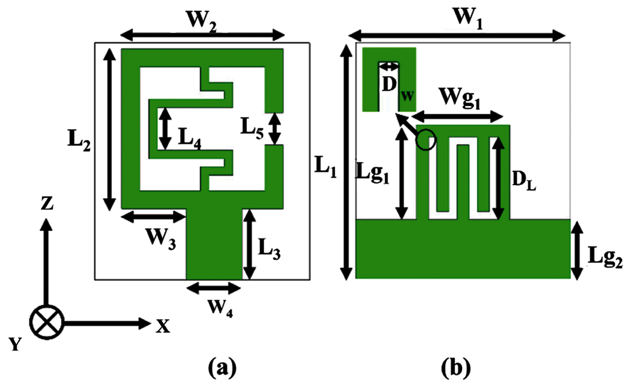
Figure 1: The configuration of the proposed antenna. (a) top view. (b) bottom view
2.1 Resonance Characteristics of the Unit Cell
The size and resonant frequency calculation of the SRR unit cell can be done using [24,25]. Initially, a square-shaped ring with length of 13.5 mm on each side and a thickness of 1.5 mm is selected. Then a split of length 0.9 mm is cut in the middle of the right side of this ring. The resonator formed in this way is anisotropic in nature i.e., it will exhibit different resonance characteristics to the incident electromagnetic wave with respect to different configurations of incident electric field vector,
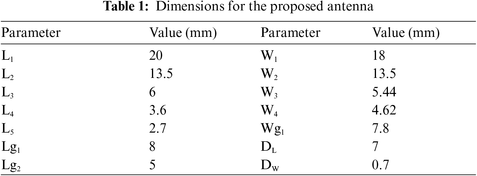
Originally, the split ring resonator exhibit mu-negative characteristic when the magnetic field is applied orthogonally to the unit cell plane, otherwise it will show epsilon-negative property [27–29] as shown in Fig. 2. However, there can be three possible configurations. Each configuration further has two different orientations after fixing the z axis.
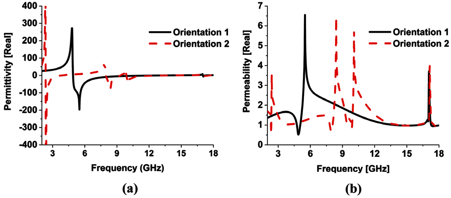
Figure 2: (a) Permittivity and (b) permeability of configuration (ii) for different orientations
The configurations of the field vectors are given below:
1. The
2. The
3. The
No noticeable resonance characteristics (is not shown here) is observed for both orientations of configuration (iii) in the desired frequency range. On the other hand, configuration (i) is not investigated here since the electric polarization found in this case is not stronger than configuration (ii). Moreover, in this research microstrip feed line is used to excite the resonator where the perpendicular component of the magnetic field of the incident electromagnetic radiation is negligible [30]. For these reasons, this excitation will not reflect the results of configuration (i).
On the contrary, the resonance behavior of the unit cell for configuration (ii) can be achieved easily by exciting the unit cell antenna with a microstrip feed line. The orientations of configuration (ii) and their transmission spectrum are shown in Fig. 3. In both orientations, the wave vector
In orientation 2,
Figure 3: Transmission spectrum of the single-split resonator. (a) orientation 1. (b) orientation 2
The current distribution of the unit cell for these orientations at the resonance frequencies is also investigated to clarify the resonance characteristics (Fig. 4). For orientation 1, an odd number of current nodes are found in the current density distribution at the resonance frequencies where the number of nodes increases with resonance frequency. Three and seven current nodes are observed in the successive excitation modes (a current node is referred to as the junction of two current paths or the starting or ending of a current path). Whereas even number of current nodes are found in the current density distributions at resonance frequencies of orientation 2. Like orientation 1 the number of nodes also increases with resonance frequency except for the second and third dips. That's why they correspond to the same excitation mode. However, two, four, and eight current nodes are observed at successive resonance frequencies.
2.2 Unit Cell Antenna Formation and Analysis
After investigating the resonance characteristics of the split ring resonator unit cell, it can be said that if the unit cell is excited in a way such that strong electric polarization is observed along with the split as orientation 2, then similar resonance characteristics will be observed. For this purpose, a microstrip feed line is connected at the center of the side which is orthogonal to the split bearing side to excite the unit cell. In the simulation, strong electric polarization is observed along with the split (Fig. 5a) and the three dips similar to orientation 2 of configuration (ii) can be obtained easily for different ground plane sizes almost at the same frequency positions as the unit cell within the frequency range of 2 to 12 GHz (Fig. 6a).
It should be noted that in this configuration because of the strong electric polarization along the split only even modes of resonances will be excited where the resonances at high frequency will cause an increased even number of current nodes in the patch. On the other hand, if the feed is connected at the middle of the non-split bearing side [not shown here] then electric polarization will not be observed along the split. And in this case, odd modes of resonances will be excited. However, in both cases, the creation of additional current nodes in the patch, which will cause higher even or odd mode resonances, can be controlled using different ground plane structures [discussed in detail in DGS section]. Now the antenna (Antenna 1) formed using the feed orientation as shown in Fig. 5a and ground structure as shown in Fig. 5b causes low frequency resonance as shown in Fig. 6b but the bandwidth is very low at the lowest mode of resonance. Since compactness is required, techniques are applied to enhance the bandwidth of the resonance at 2.4 GHz.
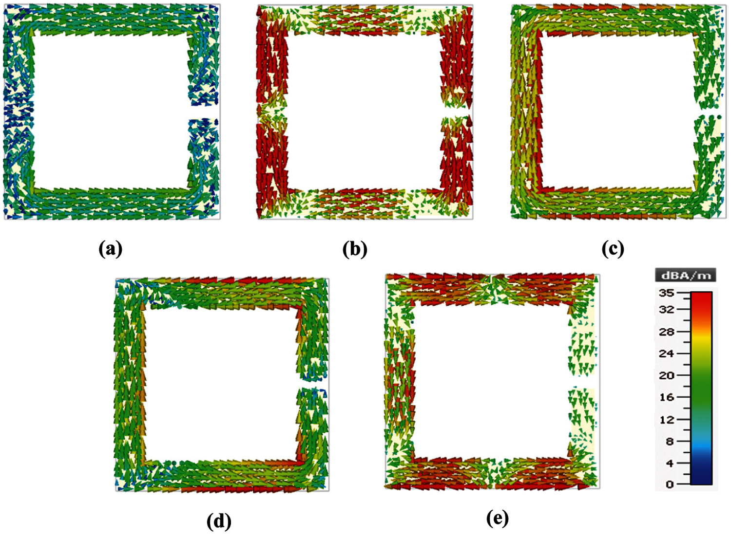
Figure 4: Current density at (a) 5.5 GHz for orientation 1. (b) 17 GHz for orientation 1. (c) 2.4 GHz for orientation 2. (d) 8.4 GHz for orientation 2. (e) 17 GHz for orientation 2
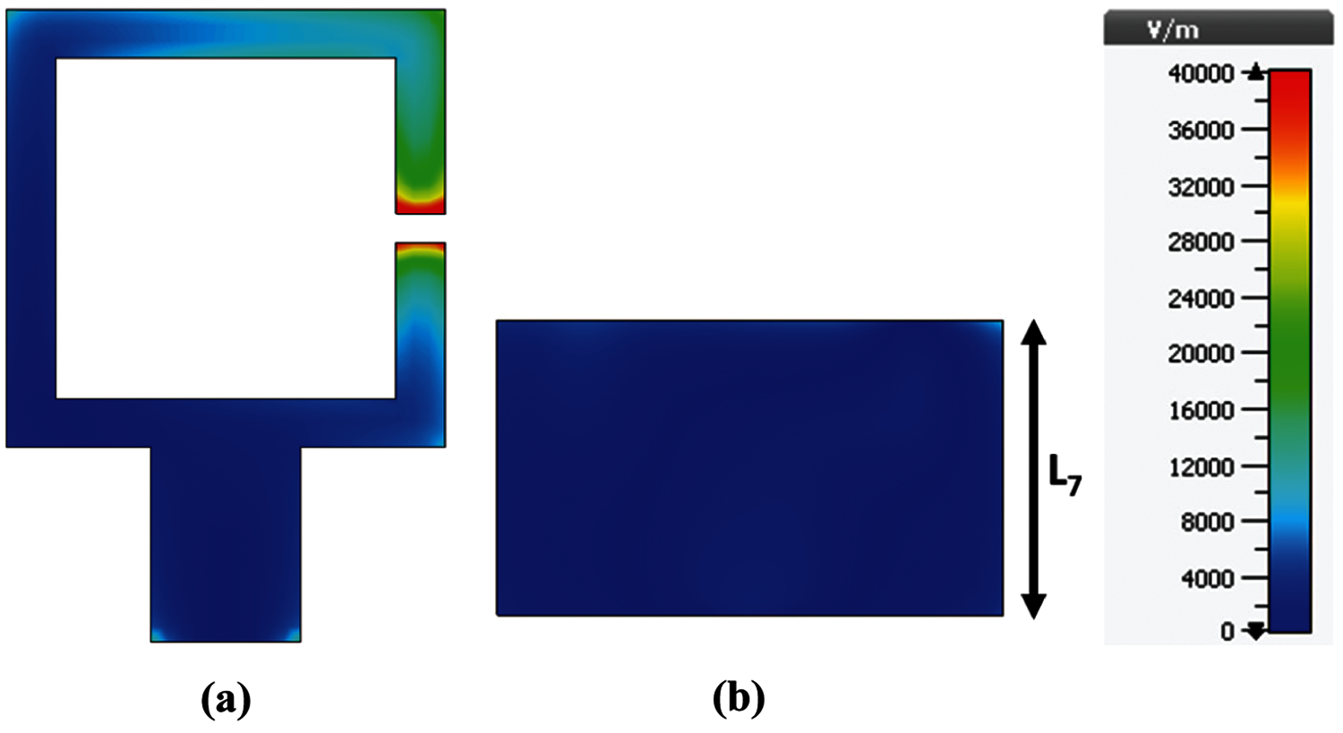
Figure 5: (a) Electric field distribution on the (a) patch and (b) ground of antenna 1 at 2.5 GHz
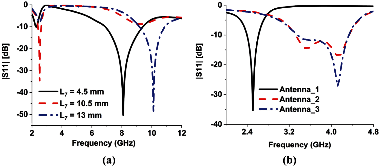
Figure 6: (a) Reflection coefficient of antenna 1 for different ground plane sizes. (b) comparison of reflection coefficient of 3 stages of the proposed antenna
First of all, a meander line is placed inside the unit cell which is parallel to the split bearing side. This structure causes the resonance to shift to the higher frequency region with a conventional ground plane. But when the novel meander line defect is loaded on the ground plane the unit cell loaded with the meander line excite another higher mode of resonance. Parameters are optimized for the proper placement of these two resonances to enhance the bandwidth. The width of the meander line and the split width are optimized to control the position of the first mode of resonance. And the width and the length of the meander line defect in the ground plane are optimized to control the position of the second mode of resonance. Finally, the feed is moved to an offset position to improve the impedance matching without affecting the bandwidth. The design evolution of the proposed antenna is shown in Fig. 7. A comparison of the reflection coefficient of different stages of the proposed antenna is shown in Fig. 6b. A detailed analysis of the techniques is given in the successive sections where parametric analysis is done to optimize the values of the parameters. It should be noted that during the parametric analysis on a particular parameter the values of other parameters are kept constant at their optimized values.
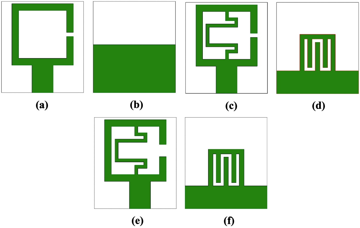
Figure 7: Design evolution of the proposed antenna. (a) patch of antenna 1. (b) ground of antenna 2. (c) patch of antenna 2. (d) ground of antenna 2. (e) patch of antenna 3. (f) ground of antenna 3
The addition of meander line inside the resonator forms two loops inside the unit cell. Since the loops are connected parallelly to each other they can be compared to two parallel loop inductances. As a result, the total inductance of the structure is reduced and the fundamental resonance is shifted to the higher frequency region.
It is well known that the inductance of a flat metal sheet depends on its width, length, and thickness [33]. So, the total inductance of the structure depends on these parameters of the meander line and the ring structure. For simplicity, only the thickness of the meander line is optimized to achieve desired resonance characteristics. A parametric analysis is done on the width of the meander line with DGS and without DGS structure (Fig. 8). It is evident from these analyses that increasing the width of the meander line will shift the first or fundamental resonance to the higher frequency for both cases and does not affect the second resonance for the case of DGS loaded ground. The optimized value of the width is 0.7 mm. The further increment will degrade the impedance matching of the resonance.
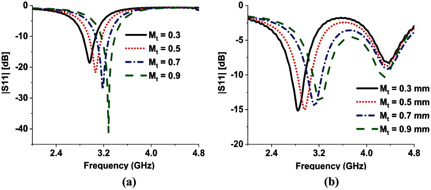
Figure 8: Parametric analysis of the meander line width (a) without DGS and (b) with DGS structure on reflection coefficient
DGS can be referred to as a compact geometry which is cut on the ground plane as a unit cell or a periodic configuration. These are resonant in nature and its’ presence beneath a printed transmission line can disturb the current on the ground plane [34,35]. For this reason, when the meander line defect is made on the ground plane, the current is gathered along the sides of the meander slots. This current induces additional current nodes at high frequency in the ring as well as in the meander line of the patch which causes an additional even mode of resonance in the high frequency.
The current distributions on the patch and the ground plane without and with DGS are shown in Figs. 9 and 10 respectively. Before adopting DGS the current on the patch follows a single direction which has only two nodes at the two ends of the split. On the other hand, the current in the portion of the ground plane which is below the patch also follows a single direction but at the corners which is not underneath the patch follows two different directions (Fig. 9). However, the opposite flows of the current at the corners of the ground do not affect the current on the patch. On the contrary, after adopting DGS on the ground plane, at low frequency the currents on the patch and the ground follow the same mechanism as without DGS [Figs. 10a and 10b]. But at high frequency, the current follows different directions in the patch which forms two additional current nodes which in turn creates four different loops (Fig. 10c). As a result, at high frequency the total inductance of the unit cell further reduces which gives rise to another higher even mode of resonance. The inductance of the loops depends on the position of the current nodes on the patch. Whereas the position of the current nodes on the patch depends on the position of the current nodes on the ground plane. That means, by controlling the position of the current node on the ground plane, the position of the higher resonance frequency can be controlled. At high frequency, the currents flow from the opposite sides of the DGS to the center causing a current node to generate at the middle top position of the structure (Fig. 10d). And it is observed from the current distribution that the positions of the current nodes on the left side of the ring as well as on the meander line are generated just above the current node position of the DGS. The length and width of the DGS are optimized to control the position of the current node on the DGS which in turn controls the position of current nodes on the patch.
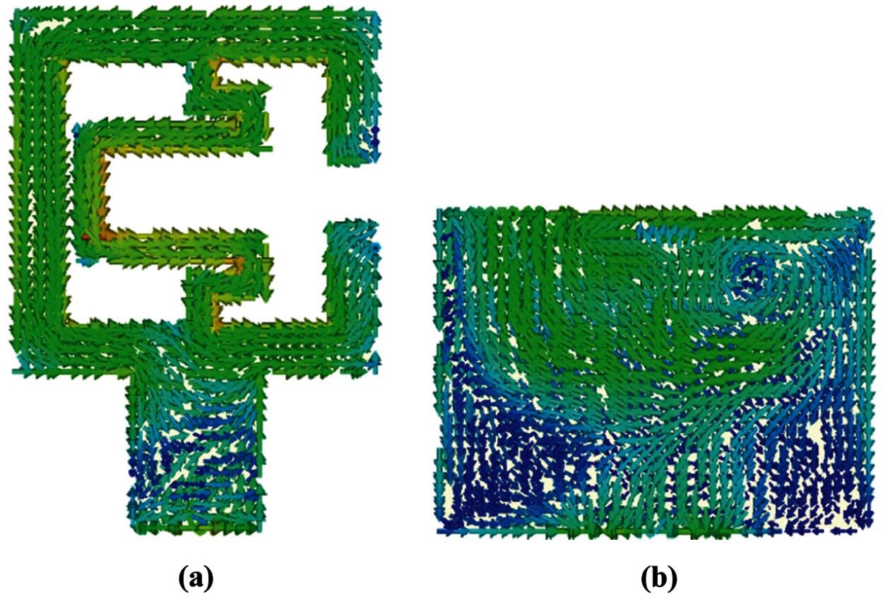
Figure 9: Current distribution without DGS (a) on the patch and (b) on the ground at 3.5 GHz
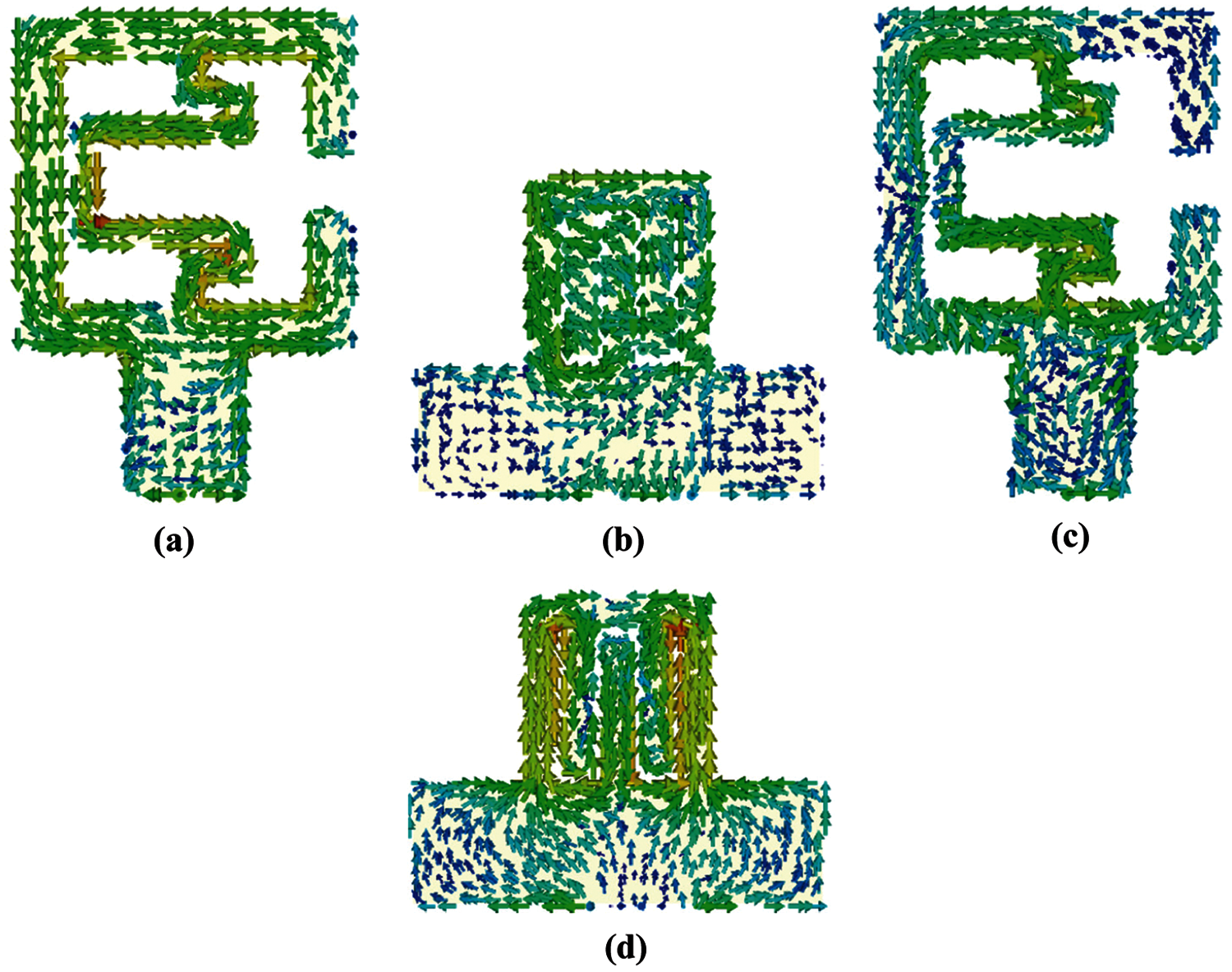
Figure 10: Current distribution with DGS (a) on the patch and (b) on the ground at 3.5 GHz. (c) on the patch and (d) on the ground at 4.13 GHz
A parametric analysis is done on the length and width of DGS to see their effect on the second resonance (Fig. 11). It is found that when the DGS length is increased the second resonance shifts to the lower frequency region with improved impedance matching but degrades the impedance matching of the first resonance. Conversely, when the DGS width is decreased the second resonance shifts to the lower frequency region with improved impedance matching but also improves the impedance matching of the first resonance. The parameters are optimized at values (DL = 7 mm, DW = 0.7 mm) for which the bandwidth is maximum.
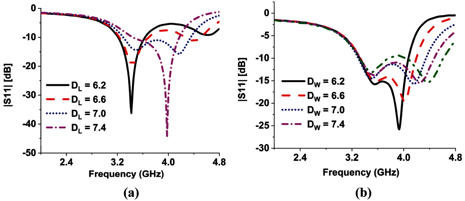
Figure. 11: Parametric analysis of the DGS (a) length and (b) width on reflection coefficient
As mentioned earlier, increasing the width of the meander line shifts the first resonance to the higher frequency but the impedance matching degrades for higher values of width. The split width is another parameter that can shift the first resonance to the higher frequency region. A parametric analysis is done on the split width to see its effect on both resonances as shown in Fig. 12a. It is found that as the value of width is increased the first resonance shifts to the higher frequency region and at the same time improves the impedance matching of the second resonance. On the other hand, it also enhances the impedance bandwidth of both bands Another parametric analysis is done on split width to see its effect on real and imaginary values of input impedance (Figs. 12b and 12c). It is found that increasing the value of the width reduces the real value of the input impedance of the first and second band at higher and lower frequencies respectively. Whereas flattens the imaginary value of them over the entire bandwidth. For this reason, two bands are placed closely with maximum impedance bandwidth. However, the width is optimized at a value (0.7 mm) where the bandwidth is maximum.
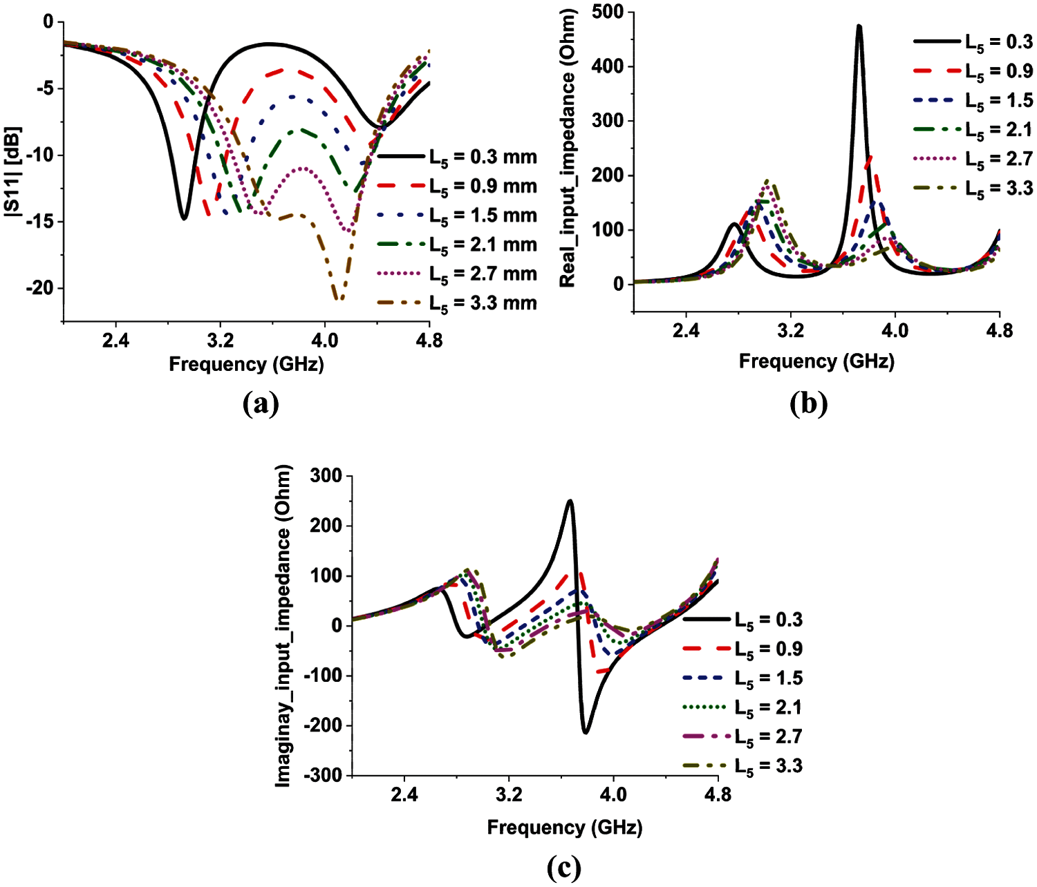
Figure 12: The parametric analysis of the split width on (a) reflection coefficient (b) real input impedance. (c) imaginary input
To verify the above analysis, a prototype of the proposed antenna is fabricated (Fig. 13) and measured. The simulated and measured reflection coefficients of the prototype as shown in Fig. 14a are in good agreement. The antenna achieves an impedance bandwidth of 26.3% for approximately |S11| < −10 dB ranging from 3.26 GHz to 4.26 GHz where only a small region within this bandwidth is found where the |S11| value fluctuate between −9 dB to −10 dB. On the other hand, the simulated result shows an impedance bandwidth of 25.75% ranging from 3.35 GHz to 4.34 GHz. This small mismatch may be caused due to the error on soldering or fabrication. The simulated realized gain varies from 0.37 dBi to 1.35 dBi within the bandwidth. Whereas the measured realized gain ranges from −0.7 dBi to 1.26 dBi which is in good agreement with the simulated data (Fig. 14b). The simulated and measured radiation patterns at 4 GHz of the proposed antenna are given in Fig. 15 which are in good agreement. From the radiation patterns in both planes, it is evident that maximum radiation occurs near the split bearing side. However, the H-plane radiation pattern is quasi-omnidirectional with low cross-polarization level. Both the simulated and measured cross polarization levels are recorded less than −15 dB in this plane.
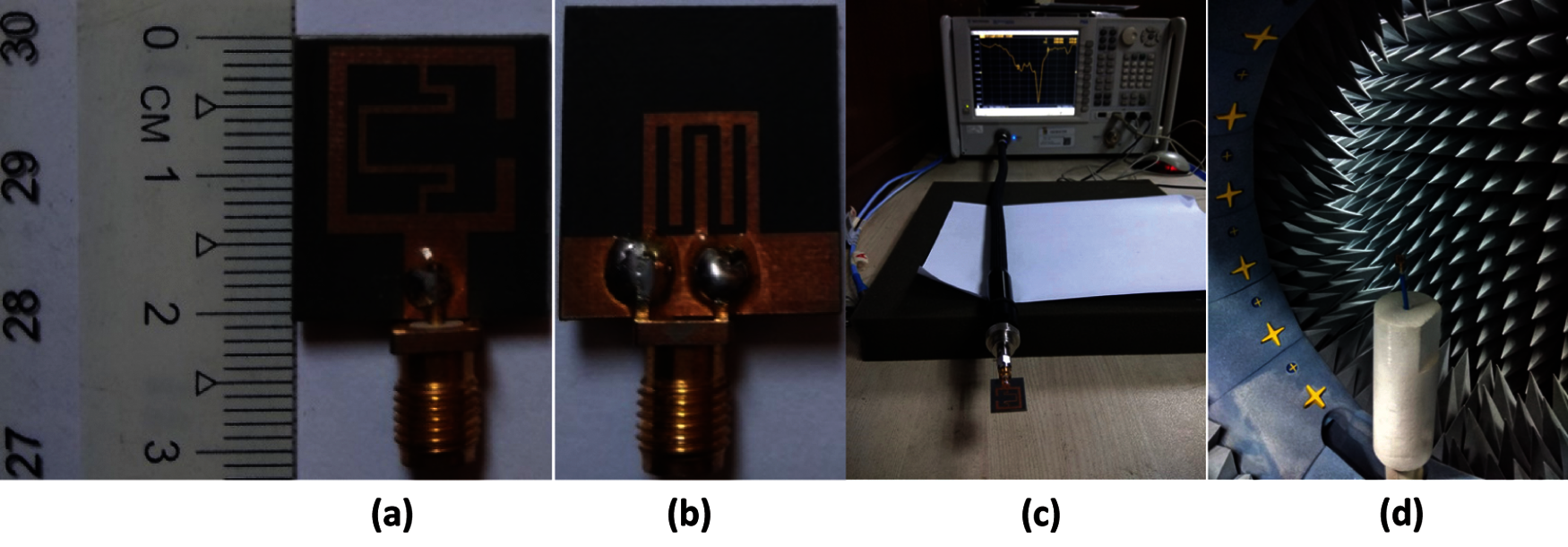
Figure 13: (a) Front side and (b) Back side of the antenna. (c) VNA measurement setup. (d) Satimo measurement setup
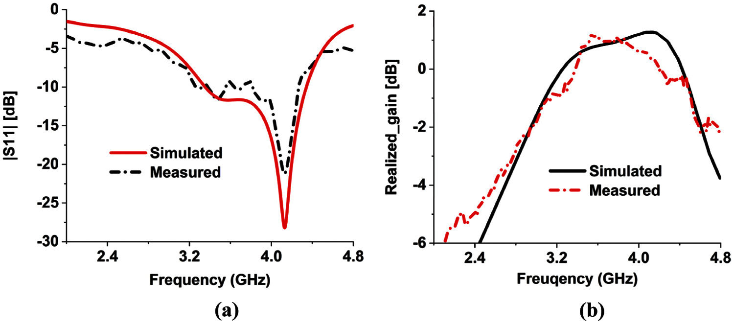
Figure 14: The simulated and measured (a) reflection coefficient and (b) realized gain of the proposed antenna
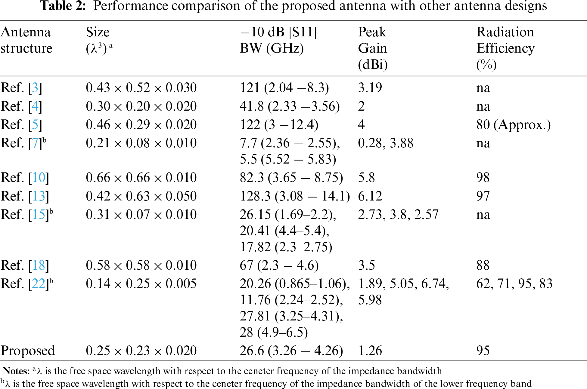
A comparison between the proposed antenna with the other reported compact antennas is presented in Tab. 2 in terms of bandwidth, size and peak gain. From the table, it is evident that the state-of-the-art antenna is more compact than compact wideband antennas and exhibits wider bandwidth than compact multiband antennas. So, further investigation on this area needs to be carried out to achieve a more miniaturized wideband radiator.
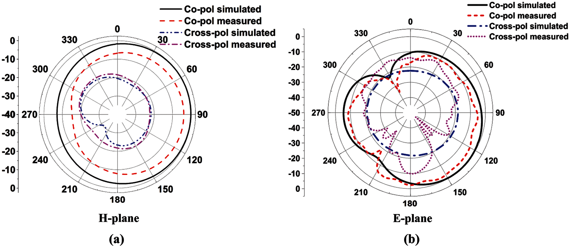
Figure 15: Simulated and measured radiation patterns of the proposed antenna. (a) XY-plane. (b) XZ-plane
In this paper, a compact, broadband SRR unit cell antenna loaded with meander line and DGS structure is designed, analyzed and tested. The unit cell of the SRR structure is used as the main radiating element of the antenna which gives low frequency resonance. The compact size of antenna 1 is almost one-seventh of the wavelength at 2.4 GHz. The utilization of the meander line loading inside the unit cell and the meander line defect on the ground plane cause the fundamental resonance and one higher even mode resonance to occur at different frequencies with proper frequency intervals. The split width is optimized to improve the input impedance over the entire bandwidth. The prototype exhibits almost an impedance bandwidth of 26% where the gain variation is not more than 1.35 dBi. But the size is increased a little bit which is almost one-fifth of the wavelength at 3.26 GHz. However, the analysis presented here can be utilized in future unit cell antenna design for small portable devices. Moreover, the prototype achieves a small cross-polarization level with almost stable omnidirectional radiation pattern in the horizontal plane. This is a great achievement with metamaterial structure and DGS loaded ground plane since both of which can deteriorate the radiation pattern. Overall, the state-of-the-art design is compact and simple which exhibits wideband property with a small variation of gain within the bandwidth and gives a stable radiation pattern. Therefore, it can be a perfect candidate for IoT and smart embedded applications for 5G sub 6 GHz band and the outcome of this research will have a great impact in future micro device evolution.
Funding Statement: The authors received no specific funding for this study.
Conflicts of Interest: The authors declare that they have no conflicts of interest to report regarding the present study.
1. W. Hu, J. J. Wu, S. F. Zheng and J. Ren, “Compact acs-fed printed antenna using dual edge resonators for tri-band operation,” IEEE Antennas and Wireless Propagation Letters, vol. 15, pp. 207–210, 2016. [Google Scholar]
2. M. Moosazadeh and S. Kharkovsky, “Compact and small planar monopole antenna with symmetrical L- and U-shaped slots for WLAN/WiMAX applications,” IEEE Antennas and Wireless Propagation Letters, vol. 13, pp. 388–391, 2014. [Google Scholar]
3. S. S. Al-Bawri, M. T. Islam, M. J. Singh, E. Alyan, M. Jusoh et al., “Broadband sub−6ghz slot-based mimo antenna for 5 g nr bands mobile applications,” Journal of Physics: Conf. Series, vol. 1962, no. 1, pp. 012038, Jul. 2021. [Google Scholar]
4. X. Fang, G. Wen, D. Inserra, Y. Huang and J. Li, “Compact wideband CPW-fed meandered-slot antenna with slotted Y-shaped central element for Wi-Fi, WiMAX, and 5G applications,” IEEE Transactions on Antennas and Propagation, vol. 66, no. 12, pp. 7395–7399, 2018. [Google Scholar]
5. J. Tao and Q. Feng, “Compact ultrawideband mimo antenna with half-slot structure,” IEEE Antennas and Wireless Propagation Letters, vol. 16, pp. 792–795, 2017. [Google Scholar]
6. W. C. Liu, C. M. Wu and Y. Dai, “Design of triple-frequency microstrip-fed monopole antenna using defected ground structure,” IEEE Transactions on Antennas and Propagation, vol. 59, no. 7, pp. 2457–2463, 2011. [Google Scholar]
7. S. Nandi and A. Mohan, “A compact dual-band mimo slot antenna for wlan applications,” IEEE Antennas and Wireless Propagation Letters, vol. 16, pp. 2457–2460, Jul. 2017. [Google Scholar]
8. R. Anitha, P. V. Vinesh, K. C. Prakash, P. Mohanan and K. Vasudevan, “A compact quad element slotted ground wideband antenna for mimo applications,” IEEE Transactions on Antennas and Propagation, vol. 64, no. 10, pp. 4550–4553, 2016. [Google Scholar]
9. N. A. Nguyen, M. Radfar, A. Ebrahimi, D. V. Ngo, A. Bervan, H. V. Le et al., “Wideband compact triangle-slot antenna with out-of-band rejection,” IEEE Antennas and Wireless Propagation Letters, vol. 19, no. 6, pp. 921–925, 2020. [Google Scholar]
10. U. Ullah, S. Koziel and I. Ben Mabrouk, “A simple-topology compact broadband circularly polarized antenna with unidirectional radiation pattern,” IEEE Antennas and Wireless Propagation Letters, vol. 18, no. 12, pp. 2612–2616, 2019. [Google Scholar]
11. M. S. Ellis, Z. Zhao, J. Wu, X. Ding, Z. Nie et al., “A novel simple and compact microstrip-fed circularly polarized wide slot antenna with wide axial ratio bandwidth for c-band applications,” IEEE Transactions on Antennas and Propagation, vol. 64, no. 4, pp. 1552–1555, 2016. [Google Scholar]
12. L. Li, X. Zhang, X. Yin and L. Zhou, “A compact triple-band printed monopole antenna for wlan/wimax applications,” IEEE Antennas and Wireless Propagation Letters, vol. 15, pp. 1853–1855, 2016. [Google Scholar]
13. S. S. Al-Bawri, H. Hwang Goh, M. S. Islam, H. Y. Wong, M.F. Jamlos et al., “Compact ultra-wideband monopole antenna loaded with metamaterial,” Sensors (Switzerland), vol. 20, no. 3, pp. 796, 2020. [Google Scholar]
14. N. K. Darimireddy, R. R. Reddy and A. M. Prasad, “A miniaturized hexagonal-triangular fractal antenna for wide-band applications [antenna applications corner],” IEEE Antennas and Propagation Magazine, vol. 60, no. 2, pp. 104–110, 2018. [Google Scholar]
15. S. Padmanathan, A. A. Al-Hadi, P. J. Soh and S. S. Al-Bawri, “Dual monopole frequency reconfigurable antenna for mimo 5 g sub−6 GHz mobile terminal,” Journal of Physics: Conf. Series, vol. 1962, no. 1, pp. 012042, 2021. [Google Scholar]
16. L. Wang, M. Q. Yuan and Q. H. Liu, “A dual-band printed electrically small antenna covered by two capacitive split-ring resonators,” IEEE Antennas and Wireless Propagation Letters, vol. 10, pp. 824–826, 2011. [Google Scholar]
17. K. Xu, F. Liu, L. Peng, W. S. Zhao, L. Ran et al., “Multimode and wideband printed loop antenna based on degraded split-ring resonators,” IEEE Access, vol. 5, pp. 15561–15570, 2017. [Google Scholar]
18. K. E. Kedze, H. Wang and I. Park, “Compact broadband omnidirectional radiation pattern printed dipole antenna incorporated with split-ring resonators,” IEEE Access, vol. 6, pp. 49537–49545, 2018. [Google Scholar]
19. P. L. Chi and Y. Sen Shih, “Compact and bandwidth-enhanced zeroth-order resonant antenna,” IEEE Antennas and Wireless Propagation Letters, vol. 14, pp. 285–288, 2015. [Google Scholar]
20. P. W. Chen and F. C. Chen, “Asymmetric coplanar waveguide (acpw) zeroth-order resonant (zor) antenna with high efficiency and bandwidth enhancement,” IEEE Antennas and Wireless Propagation Letters, vol. 11, no. 2, pp. 527–530, 2012. [Google Scholar]
21. H. Lee, D. J. Woo and S. Nam, “Compact and bandwidth-enhanced asymmetric coplanar waveguide (acpw) antenna using crlh-tl and modified ground plane,” IEEE Antennas and Wireless Propagation Letters, vol. 15, pp. 810–813, 2016. [Google Scholar]
22. S. S. Al-Bawri, M. S. Islam, H. Y. Wong, M. F. Jamlos, A. Narbudowicz et al., “Metamaterial cell-based superstrate towards bandwidth and gain enhancement of quad-band cpw-fed antenna for wireless applications,” Sensors (Switzerland), vol. 20, no. 2, pp. 457, 2020. [Google Scholar]
23. R. W. Ziolkowski, P. Jin and C. C. Lin, “Metamaterial-inspired engineering of antennas,” in Proc. of the IEEE, vol. 99, no. 10, pp. 1720–1731, 2011. [Google Scholar]
24. M. Kafesaki, T. Koschny, R. S. Penciu, T. F. Gundogdu, E. N. Economou et al., “Left-handed metamaterials: Detailed numerical studies of the transmission properties,” Journal of Optics A: Pure and Applied Optics, vol. 7, no. 2, pp. 12–22, 2005. [Google Scholar]
25. O. Sydoruk, E. Tatartschuk, E. Shamonina and L. Solymar, “Analytical formulation for the resonant frequency of split rings,” Journal of Applied Physics, vol. 105, no. 1, pp. 1–5, 2009. [Google Scholar]
26. S. Zahertar, A. D. Yalcinkaya and H. Torun, “Rectangular split-ring resonators with single-split and two-splits under different excitations at microwave frequencies,” AIP Advances, vol. 5, no. 11, pp. 117220, 2015. [Google Scholar]
27. N. Engheta and R. W. Ziolkowski, in Metamaterials: Physics and Engineering Explorations, USA: Wiley-IEEE Press, 2006. [Google Scholar]
28. I. K. Kim and V. V. Varadan, “Electric and magnetic resonances in symmetric pairs of split ring resonators,” Journal of Applied Physics, vol. 106, no. 7, pp. 074504, 2009. [Google Scholar]
29. J. Zhou, T. Koschny and C. M. Soukoulis, “Magnetic and electric excitations in split ring resonators,” Optics Express, vol. 15, no. 26, pp. 17881, 2007. [Google Scholar]
30. C. A. Balanis, “Microstrip Antennas,” in Antenna Theory: Analysis and Design, 4th ed., Hoboken, New Jersey, USA: John Wiley & Sons, 2015. [Google Scholar]
31. T. Koschny, M. Kafesaki, E. N. Economou and C. M. Soukoulis, “Effective medium theory of left-handed materials,” Physical Review Letters, vol. 93, no. 10, pp. 1–4, 2004. [Google Scholar]
32. N. Katsarakis, T. Koschny, M. Kafesaki, E. N. Economou and C. M. Soukoulis, “Electric coupling to the magnetic resonance of split ring resonators,” Applied Physics Letters, vol. 84, no. 15, pp. 2943–2945, 2004. [Google Scholar]
33. F. E. Terman, “Circuit Elements,” in Radio Engineer's Handbook, 1st ed., New York, USA: McGraw-Hill, 1943. [Google Scholar]
34. F. Yang and Y. Rahmat-Samii, Electromagnetic Band Gap Structures in Antenna Engineering, Cambridge, UK: Cambridge University Press, 2008. [Google Scholar]
35. D. Guha, S. Biswas and Y. M. M. Antar, “Defected Ground Structure for Microstrip Antennas,” in Microstrip and Printed Antennas, Chichester, UK: John Wiley & Sons, Ltd, pp. 387–434, 2010. [Google Scholar]
 | This work is licensed under a Creative Commons Attribution 4.0 International License, which permits unrestricted use, distribution, and reproduction in any medium, provided the original work is properly cited. |