DOI:10.32604/cmc.2022.022988
| Computers, Materials & Continua DOI:10.32604/cmc.2022.022988 | |
| Article |
Unified FPGA Design for the HEVC Dequantization and Inverse Transform Modules
Department of Electrical Engineering, Jouf University, Sakaka, Aljouf, 2014, Saudi Arabia
*Corresponding Author: Ahmed Ben Atitallah. Email: abenatitallah@ju.edu.sa
Received: 25 August 2021; Accepted: 03 November 2021
Abstract: As the newest standard, the High Efficiency Video Coding (HEVC) is specially designed to minimize the bitrate for video data transfer and to support High Definition (HD) and ULTRA HD video resolutions at the cost of increasing computational complexity relative to earlier standards like the H.264. Therefore, real-time video decoding with HEVC decoder becomes a challenging task. However, the Dequantization and Inverse Transform (DE/IT) are one of the computationally intensive modules in the HEVC decoder which are used to reconstruct the residual block. Thus, in this paper, a unified hardware architecture is proposed to implement the HEVC DE/IT module for all Transform Unit (TU) block size, including 4 × 4, 8 × 8, 16 × 16 and 32 × 32. This architecture is designed using the High-Level Synthesis (HLS) and the Low-Level Synthesis (LLS) methods in order to compare and determine the best method to implement in real-time the DE/IT module. In fact, the C/C++ programming language is used to generate an optimized hardware design for DE/IT module through the Xilinx Vivado HLS tool. On the other hand, the LLS hardware architecture is designed by the VHSIC Hardware Description language (VHDL) and using the pipeline technique to decrease the processing time. The experimental results on the Xilinx XC7Z020 FPGA show that the LLS design increases the throughput in term of frame rate by 80% relative to HLS design with a 4.4% increase in the number of Look-Up Tables (LUTs). Compared with existing related works in literature, the proposed architectures demonstrate significant advantages in hardware cost and performance improvement.
Keywords: HEVC decoder; dequantization; IDCT/IDST; LLS design; HLS design; FPGA
Nowadays, several consumer electronic devices such as television [1], smartphone [2], tablet [3], etc use video standard codec for video compressing and transmitting data with minimum bitrate. In this context, a High Efficiency Video Coding (HEVC) video standard is developed [4,5]. The HEVC is a video compression standard that can provide a good performance than the previous standard, i.e., H.264/AVC [6]. In fact, it can support a high video resolution which can reach to 8K (7680 × 4320) and reduces the bitrate approximately by 50% relative to H.264/AVC [7,8] with same video quality.
In video standard codec the Dequantization and Inverse Transform (DE/IT) play a very important role to reconstruct the compressed video sequences [9]. Nevertheless, in HEVC video decoder, the DE/IT module allows to reconstruct the residual block which can be with several size 4 × 4, 8 × 8, 16 × 16, and 32 × 32. In fact, the largest coding unit in HEVC can be up to 64 × 64 in size, and the Transform Unit (TU) sizes can be 4 × 4, 8 × 8, 16 × 16, and 32 × 32 [10]. This multiple TU sizes improve the compression performance but increase the computational complexity to reach a real-time execution [11,12]. In this context, based on the complexity analysis of the HEVC decoder modules for all-intra configuration performed in [13], we can notice that the entropy decoding (ED), the intra prediction (IP) and the DE/IT modules consume on average 38%, 32% and 20% of the total decoding time, respectively. However, according to the analysis given in [14] for the ED module, it is obviously that the computational complexity presented in the regular CABAC algorithm makes it difficult to be pipelined and parallelized in such hardware context. This complexity is caused by the critical bin-to-bin data dependencies and the use of feedback between entropy decoding steps. On the other hand, we have proposed in [13] a hardware architecture to implement the IP block. For this reason, we focus in this work to propose an efficient hardware design to reduce the computational complexity of the HEVC DE/IT module.
Recently, field-programmable gate arrays (FPGAs) have been gaining popularity for image and video processing. Indeed, modern FPGAs have sufficient resources to implement a complex application [15,16]. The traditional approach used to design and implement any algorithm in FPGA is Low-Level Synthesis (LLS) using hardware description language (HDL) such as VHSIC hardware description language (VHDL or Verilog). With such low-level design, it is possible to adjust the Register Transfer Level (RTL) description to generate an optimized hardware architecture [17–19]. But, this kind of design requires a lot of time and effort specially for complex algorithm. To alleviate this problem, the High-Level Synthesis (HLS) is introduced [20–22]. Nevertheless, the HLS flow uses the high-level programming language like C/C++, systemC, etc to generate automatically the RTL design. This approach makes the code more readable, shortens design and verification times, and increases the design reusability over those of handwritten HDL equivalents.
In literature, many architectures are proposed to implement the dequantization and inverse transform modules for HEVC decoder. In fact, the design outlined in [23] presents an FPGA implementation of the HEVC 2D integer inverse discrete cosine transform (2D-IDCT) using different HLS tools. The developed design can decode 54 frames/sec (FPS) for 1080p video sequences. In [24], the authors provide a System-On-Chip FPGA platform based on Xilinx Zynq to integrate the DCT coding block as an accelerator with HLS tool. The proposed design is capable to perform the coding of 1080@30fps. In [25], a LLS hardware architecture for 2D-IDCT is proposed. This architecture can process 4K@28fps at 135 MHz under XC7Z045 Xilinx FPGA. In addition, Chen et al. [26] design a 2D-IDCT architecture that supports all TU sizes. This architecture can calculate two rows in parallel during the 1D-IDCT instead of only one. In this case, the maximum throughput achieved is about 4K@30fps with the Xilinx Zynq platform. But Liang et al. [27] present an architecture that supports the 2D integer inverse discrete sine transform (2D-IDST) and 2D-IDCT using two 1D-IDCT/IDST units and memory block. This architecture calculates four residual pixels in parallel in each clock cycle. This design can decode 7680 × 4320@30fps. In [28] a hardware implementation of the 2D dequantization, IDCT and IDST (2D-DE/IDCT/IDST) for HEVC decoder is described. The proposed architecture can perform the decoding of 4K@30fps at 200 MHz clock frequency in TSMC 40 nm technology. However, such implementation presents a good compromise in terms of energy efficiency, resources utilization and performance but miss flexibility in term of programmability. On the other, in [29] an efficient OpenCL implementation of the HEVC 2D-DE/IDCT/IDST module is proposed. This software implementation is realized based on an exploitation of the parallel processing offered by modern Graphic Processing Unit (GPUs). The proposed solution can decode 4K@15fps on GeForce GTX 780Ti@1046 MHz. This implementation preserves the flexibility and accuracy of software but with an increase in power consumption.
Hence, the aim of this paper is to provide a unified and optimized hardware architecture to implement the 2D-DE/IDCT/IDST module for HEVC decoder. This architecture should support 4 × 4, 8 × 8, 16 × 16 and 32 × 32 HEVC TU block size and offer a trade-off between performance, hardware cost and processing time. For this, the LLS and HLS design flow are used and explored to design a hardware architecture for HEVC 2D-DE/IDCT/IDST module. However, the HLS 2D-DE/IDCT/IDST design is explored through the Xilinx Vivado HLS 2018.1 tool by adding specific directives (e.g., PIPILINE, RESSOURCE, etc) to the high level programming language such as C/C++ code. But, the LLS 2D-DE/IDCT/IDST design is developed by using the pipeline technique through the VHDL language. The hardware architectures for both methods are mapped and evaluated on Xilinx XC7Z020 FPGA for processing time and hardware cost in order to determine which design method (LLS or HLS) provides better design productivity when facing a complex algorithm like the 2D-DE/IDCT/IDST module for HEVC decoder.
The remainder of the paper is structured as follows. Section 2 introduces an overview of HEVC 2D-DE/IDCT/IDST module. Section 3 describes the hardware architecture designed for 2D-DE/IDCT/IDST module using HLS and LLS design flow. The implementation results and performance evaluation are reported in Section 4. Finally, Section 5 concludes the paper.
2 Dequantization and Inverse Transform in HEVC Decoder
In HEVC, each frame is partitioned into coding tree block structure involving different sizes of large coding units (LCUs) up to 64 × 64. As illustrated in Fig. 1, each LCU can be recursively split into several sizes of coding units (CUs). Starting from a defined partition of CUs, it is possible to further generate two other types of units corresponding to prediction unit (PU), which is used for inter/intra prediction processes, and TU, which is the elementary unit of dequantization and inverse transform. However, the size of the TU block is defined by HEVC encoder and can be 4 × 4, 8 × 8, 16 × 16 and 32 × 32.
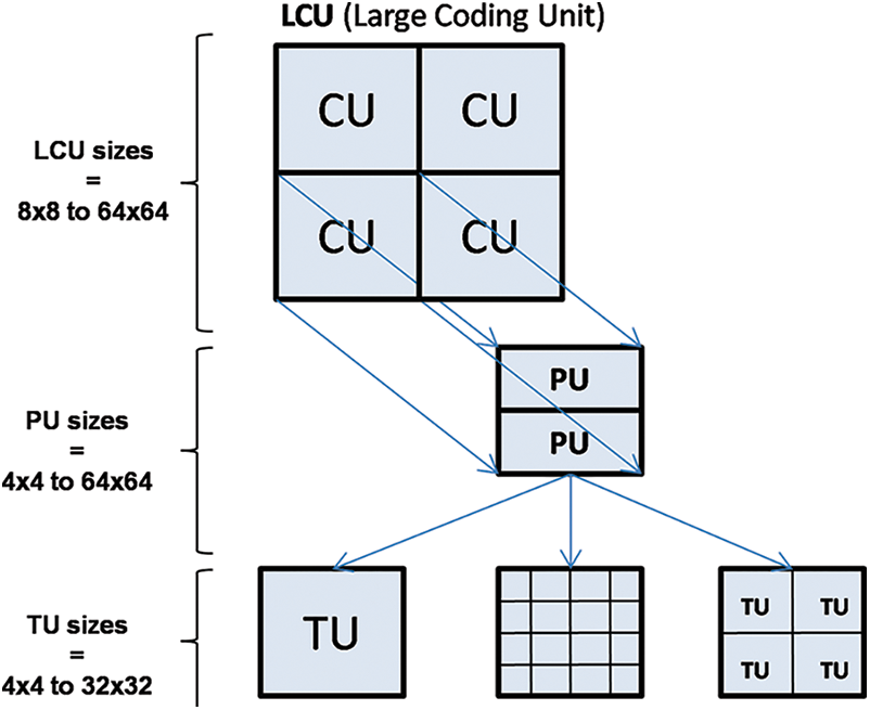
Figure 1: Coding structure in HEVC standard
Thus, the 2D-DE/IDCT/IDST module receives the coefficients of the TU block from the entropy decoder and applies the dequantization to restore the original Transform coefficients. The dequantization scheme as specified be HEVC is given by Eq. (1).
where coeffDQ is the dequantized coefficient, level is the quantized DCT coefficient, QP is the quantization parameter ranged from 0 to 51 (every TU has its own QP value), N is the size of TU block, B is the bit depth and the function f(QP%6) is determined from Tab. 1. The coeffDQ is clipped to the range [−32768, 32768] to guarantee that the dequantized coefficient is computed with 16-bit.

After dequantization, the 2D-IDCT is performed. In fact, the IDCT module takes dequantized coefficient and performs as two separate 1D-IDCT to obtain is outputs the residual block. The HEVC decoder supports two types of inverse transform which are IDCT and IDST. The IDST is applied only to the 4 × 4 TU block. During decoding, the transformed coefficients are converted back to the spatial domain via an inverse transform. According the HEVC, the 2D-IDCT/IDST can be expressed by Eq. (3).
where SRC is the transformed block, DST is the residual block and M is a N×N IDCT/IDST coefficient matrix which defined by HEVC standard. The value N is depending of the TU size. For each TU size, it has its own transform matrix. But, the 32 × 32 TU's transform matrix includes other sizes TU's transform matrix. In HEVC, the 2D-IDCT/IDST is computed by two 1D-IDCT/IDST where a column inverse transform is followed by a row inverse transform.
To decrease the implementation complexity of 2D-IDCT/IDST, Chen et al. [30] was proposed a fast algorithm for transform by decomposing the transform matrix MN to some zero matrixes. This decomposition technique is presented by Eq. (4).
where PN is the permutation matrix. BN is the N-point butterfly structure. MN,odd and MN,even are the odd and even parts of MN, respectively. For example, Eq. (5) illustrates the 8 × 8 coefficient matrix in HEVC and Eq. (6) the decomposition of this matrix. Fig. 2 presents the flowchart of 8-points 1D-IDCT based on Chen's algorithm.
where:
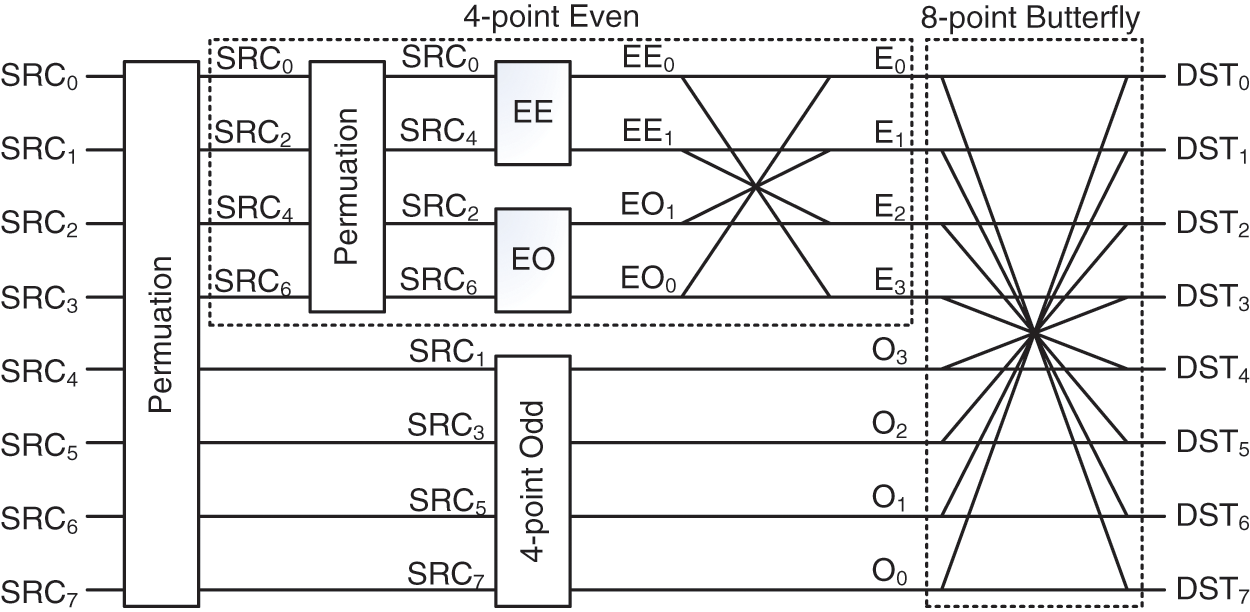
Figure 2: Flowchart of 8-points 1D-IDCT based on chen's algorithm
3 2D-DE/IDCT/IDST Hardware Architecture
In this section, we describe the HLS and LLS hardware architectures designed to implement the HEVC 2D-DE/IDCT/IDST algorithm on Xilinx XC7Z020 FPGA. In this work, the HEVC test Model (HM16.0) [31] is used as reference software.
3.1 HLS 2D-DE/IDCT/IDST Hardware Architecture
HLS is gaining more and more popularity specially when using FPGA circuit. Nevertheless, with HLS, it becomes possible to reduce the conception and validation time of the hardware design. Therefore, the exploration and the simulation of multiple hardware architectures can be done in the shortest time. But, HLS requests designers to restructure programs, change a source code and add a specific directive to get a good result. In this context, Xilinx developed the Vivado HLS tool. This tool accepts as input a high-level programming language such as C/C++ and generates automatically as output an RTL hardware description. Through this tool, it is possible to add several directives (such as LOOP unrolling, ALLOCATION, RESOURCE, etc) in order to generate an optimize RTL design in terms of hardware cost and processing time.
For the HLS implementation of the HEVC 2D-DE/IDCT/IDST module, the C code of this module is extracted from HM16.0. The 2D-DE/IDCT/IDST algorithm is implemented with HLS based on the algorithm proposed in Fig. 3. In fact, some characteristics are taken account in this algorithm to reduce the hardware cost and complexity and generate a performant HLS design for 2D-DE/IDCT/IDST module. However, the HLS design supports 4/8/16/32 TU size. The dequantization and 2D-IDCT/IDST are integrated in one design to minimize the processing time. Moreover, the even-odd 1D-IDCT/IDST algorithm is used as shown in Fig. 2. In addition, 8-point 1D-IDCT is computed by using 4-point IDCT (even part), 4-point odd and butterfly module. Even for 16-point IDCT is calculated based-on 8-point 1D-IDCT, 8-point odd and butterfly module. Also, 32-point IDCT is determined from 16-point 1D-IDCT, 16-point odd and butterfly module. Further, all multiplication operations in 1D-IDCT/IDST are replaced by shift and addition based on the study realized in [25]. Furthermore, 1D-IDCT/IDST module is called two time and the intermediate memory block is used to save and transpose coefficients to generate 2D-IDCT/IDST. All these characteristics allow to reduce the hardware cost and hardware complexity.
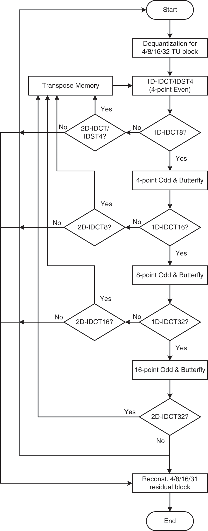
Figure 3: Dataflow of the HLS 2D-DE/IDCT/IDST module for HEVC decoder
However, in the beginning, the HLS architecture receives as input the TU size, the correspond coefficients (maximum 1024 coefficients) and the QP value. Then, these coefficients are dequantized to generate the transform coefficients. After that, if the TU size is egal to 4 × 4, thus in the first step, the 1D-IDCT4/IDST4 will be applied to the columns of TU to generate the 1D-transfrom coefficients. In the second step, these coefficients are stored in transpose memory to be used for 2D-transfrom. In the last step, the 1D-IDCT4/IDST4 will be applied to the row of TU to reconstruct the residual block. But, if the TU size is equal to 8 × 8, 16 × 16 or 32 × 32, so the 4-point odd, 8-point odd and 16-point odd are used with 4-point even and butterfly module to produce 1D/2D-IDCT8/16/32 coefficients, respectively.
In order to improve the design performances, several directives are added incrementally to the HEVC 2D-DE/IDCT/IDST C code. A part of the C code developed and given as input to Xilinx Vivado HLS tool 18.1 is shown in Figs. 4 and 5 used for dequantization and 1D-IDCT8, respectively. Thus, several designs are generated to implement the 2D-DE/IDCT/IDST module. In fact, Design 1 is generated without adding any directive. The synthesis results on the Xilinx XC7Z020 FPGA shows that this design uses 21466 (40.3%) of Look-Up Tables (LUTs), 10252 (19.3%) of Flip-Flops (FFs), 40 (18.2%) of DSP blocks and 30 (21.4%) of BRAM as illustrated in Fig. 6 and needs in worst case 15562 clock cycles to reconstruct the 32 × 32 residual block (Fig. 7). From these results, we notice that the number of clock cycles is high. For that, the PIPELINE directive should be used to decrease the number of clock cycles. In fact, from Figs. 4 and 5, we can see that the dequantization and IDCT C codes use loop iteration to reconstruct the transom and residual coefficients. The length of the loop iterations depends of the TU size. So, the loop can reach 1024 iterations. However, the PIPLINE directive is applied to loop iterations with interval equal to 1 to reduce the cycles number of latencies required for an input data to reach its output. Consequently, the Design 2 is created. According to Figs. 6 and 7, Design 2 allows to decrease by 91% the number of clock cycles but with an important increase in the hardware cost by 45% of LUTs, 62.3% of FFs, 47.4% of DSP blocks and 44.5% of BRAMs relative to Design 1. Therefore, to reduce the hardware cost, the Design 3 is generated by using the ALLOCATION and RESSOURCE directives. Indeed, the ALLOCATION directive is added to process the multiplication operations in the level of dequantization equation which allows to share the hardware resources between several operations. Furthermore, the RESOURCE directive is used to implement the residual and dequantization arrays by a specific memory block (BRAMs). This optimization has allowed to decrease the hardware cost by 42% of LUTs, 30.8% of FFs, 42.1% of DSP blocks and 55.5% of BRAMs but with an increase by 61% in the number of clock cycles compared to Design 2 as reported in Figs. 6 and 7. On the other hand, we can constate that the Design 3 provides a decrease in number of clock cycles by about 67% in worst case but with an increase by 5% of LUTs, 45% of FFs and 9% of DSP blocks relative to Design 1. Afterward, the Design 3 is used for the comparative study with LLS 2D-DE/IDCT/IDST because it offers a trade-off between hardware cost and processing time.
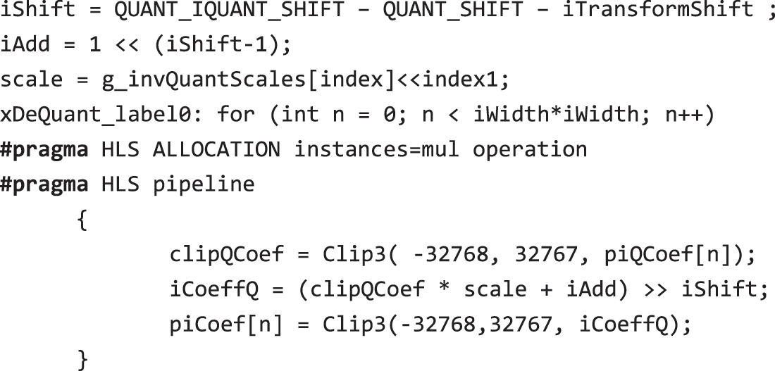
Figure 4: Dequantization Vivado HLS C code
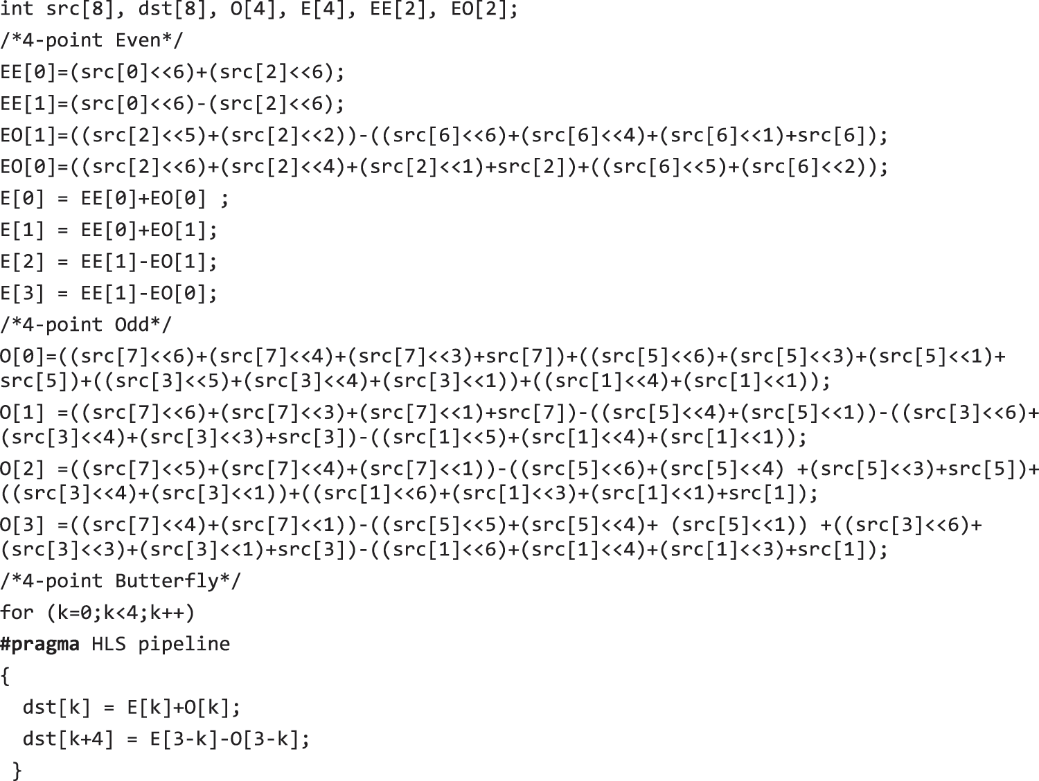
Figure 5: 8-point IDCT Vivado HLS C code
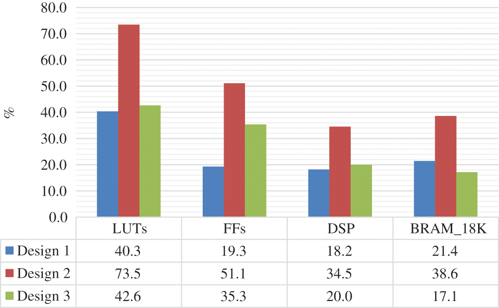
Figure 6: HLS synthesis results of HEVC 2D-DE/IDCT/IDST module
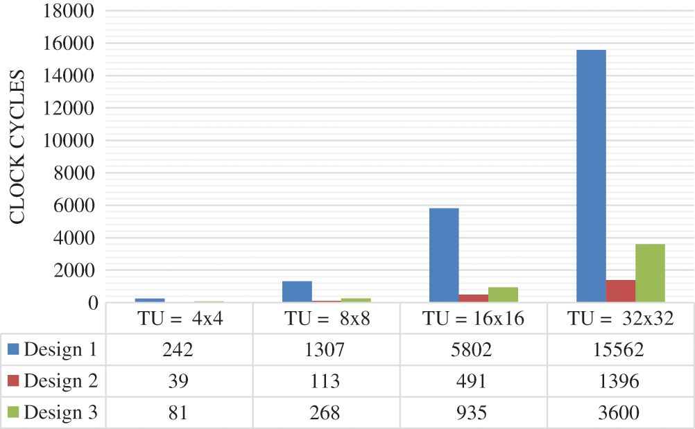
Figure 7: Number of clock cycles to reconstruct 4/8/16/32 residual block
3.2 LLS 2D-DE/IDCT/IDST Hardware Architecture
The hardware architecture depicted in Fig. 8 describes the LLS design of the HEVC 2D-DE/IDCT/IDST module. In fact, this architecture is composed by four dequantization units (Unit_DQ0, Unit_DQ1, Unit_DQ2 and Unit_DQ3), 1D-IDCT/IDST unit, transpose memory unit and control unit. It receives as input four 16-bit coefficients (Coeff0, Coeff1, Coeff2 and Coeff3) each three clock cycles from the entropy decoder, size of TU block (sel signal), QP value (QP signal) and start signal and generates as output the residual block and Done_DQ/IDCT signal which indicates that the residual block is ready. However, the designed architecture contains the dequantization and 1D-IDCT/IDST units in one design in order to benefit of the pipeline technique which can decrease the processing time.
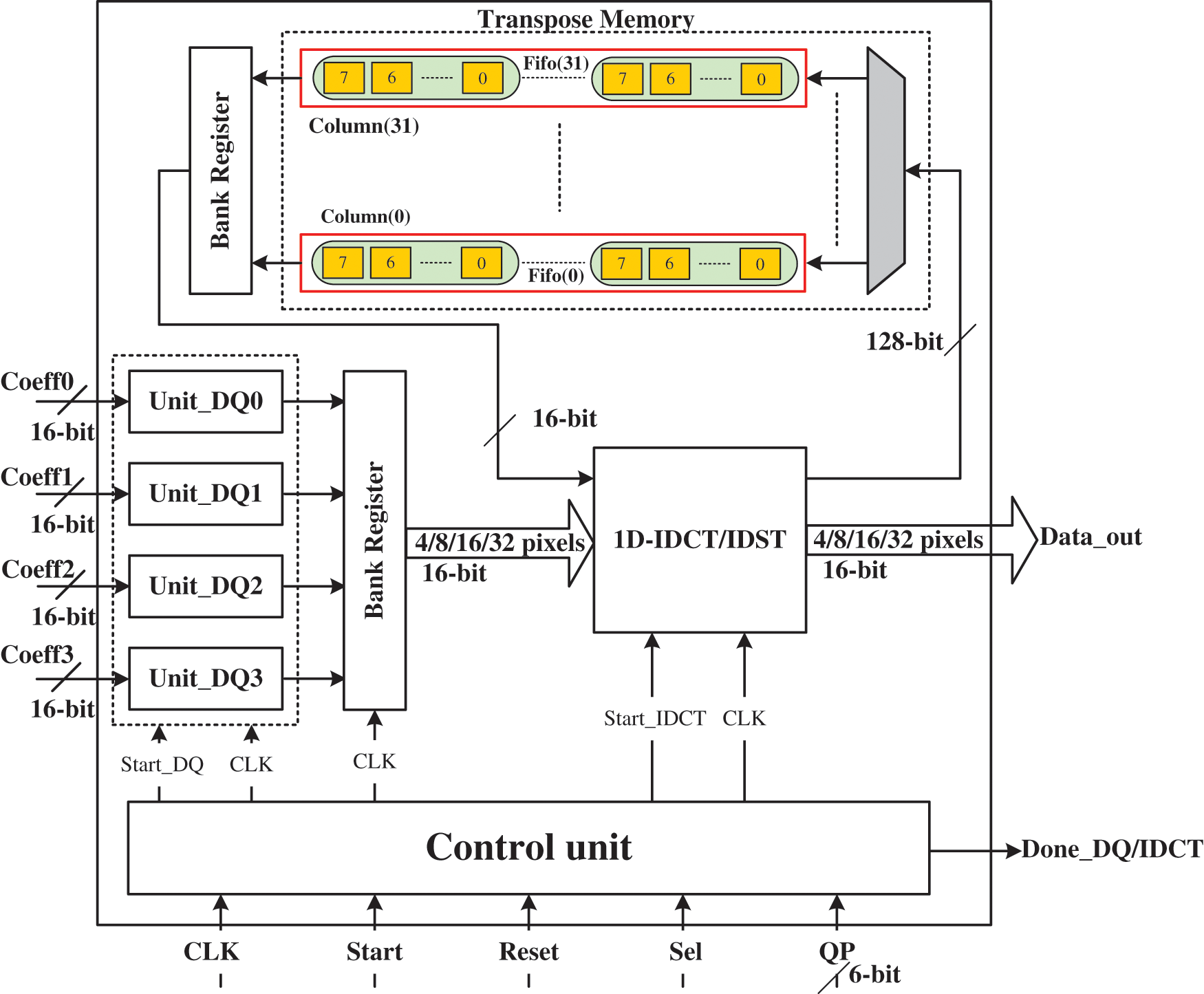
Figure 8: LLS hardware architecture for HEVC 2D-DE/IDCT/IDST module
Fig. 9 presents the hardware architecture of Unit_DQ. This architecture is developed based on Eq. (1). Indeed, two Read-Only-Memory (ROM1 and ROM2) are used to store the precalculated values proportional to QP%6 and QP/6, respectively. These memories are addressed based on QP value through the control unit. However, the 16-bit level signal receives the quantized coefficient which is multiplied by the value collected for ROM1. Then, the obtained result is shifted by the value collected from ROM2, added to the offset value and shifted by offset1. In the end, the 16-bit dequantization coefficient is obtained in two clock cycles through CoeffQ signal.
Figure 9: Hardware architecture of Unit_DQ
Fig. 10 depicts the 1D-IDCT/IDST hardware architecture. This architecture is designed to support 4 × 4, 8 × 8, 16 × 16 and 32 × 32 TU size and use even-odd IDCT decomposition. In fact, the 32-point 1D-IDCT is constructed by using a 4-point even, a 4-point odd, an 8-point odd and a 16-point odd. Moreover, to reduce the hardware cost, the multiplication operations are replaced by shift and addition. Also, when analyzing the IDCT equation, we constate that there are some repetitive coefficients (X2, X4, X9, X18, X36, X64, X90). The Xcoeff components is used to compute these coefficients which are used to deduce the other cofficients (i.e.,: X75=X64+X9+X2). However, 1D-IDCT/IDST architecture receives dequantized coefficients through 32 SRC signals and produces the transformed coefficients through 32 DST signals in 12 clock cycles, 24 clock cycles, 80 clock cycles and 160 clock cycles for 4/8/16/32 TU size, respectively.
Figure 10: 1D-IDCT/IDST hardware architecture
The transpose memory is used to store the intermediate coefficients between column and row of the inverse transform. It can store the coefficients of all TU size. The access to memory is optimized by concatenation eight 16-bit coefficients. In fact, in one clock cycles, it is possible to write and read 128-bit which mean eight coefficients in same time.
The control unit serves to share and synchronize data between all units in our design as shown in Fig. 11. Accordingly, for 4 × 4 TU size, in the first step the control unit send four 16-bit coefficients (1st column) to the dequantized units. Then, in the second step, the dequantized units receive the 2sd column after 3 clock cycles and the 1D-IDCT4/IDST4 process the 1st column in 3 clock cycles. After that, in the third step, 1st column is concatenated and stored in transpose memory in one clock cycle, the 2sd column is processed by inverse transform in 3 clock cycles and the 3th column is treated by the dequantized units in 2 clock cycles. Thus, the pipeline technique is used between all units to optimize the processing time. So, for 4 × 4 TU size, firstly the TU is processed column by column by dequantized units and 1D-IDCT4/IDST4 and the output coefficients for each column are stored in transpose memory. This step needs 16 clock cycles. Then, the 1D-IDCT4/IDST4 is performed again row by row from transpose memory. In the end, the DE/IDCT of 4 × 4 TU size is obtained in 29 clock cycles. All these steps are used for 8/16/32 TU size and need 77 clock cycles, 280 clock cycles and 938 clock cycles, respectively as shown in Fig. 11.
Figure 11: Timing diagram for HEVC 2D-DE/IDCT/IDST module
4 Implementation Results and Performance Evaluation
Tab. 2 conducts a comparison of the synthesis results, number of clock cycles and clock frequency for HLS and LLS 2D-DE/IDCT/IDST designs under XC7Z020 FPGA for 4 × 4, 8 × 8, 16 × 16 and 32 × 32 TU size. It can be seen from this table that the HLS design uses less LUTs by 4.4% but more FFs, RAMs and DSPs by 9.5%, 5.7% and 18.2%, respectively, relative to LLS design. Moreover, the LLS design allows to reduce the number of clock cycles by 64% compared to HLS design.
On the other hand, the performance of HLS and LLS design for HEVC 2D-DE/IDCT/IDST is measured for several class of video sequences such as Class A (2560 × 1600), Class B (1920 × 1080), Class C (1280 × 720) and Class D (832 × 480). So, from Fig. 12, we can see that the frame rate of LLS design can reach 339 fps for class D and 33 fps for class A instead of 66 fps for class D and 6 fps for class A using HLS design. However, with LLS design the frame rate is increased by 80% relative to HLS design in worst case as shown in Fig. 13.
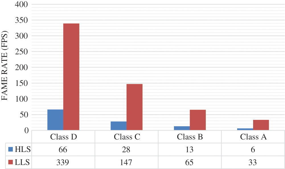
Figure 12: Frame rate comparison between HLS and LLS designs for A, B, C and D video class
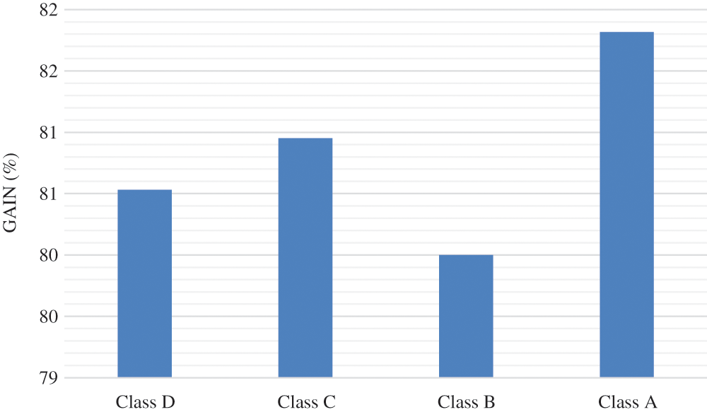
Figure 13: Gain in frame rate for LLS relative to HLS for A, B, C and D video class
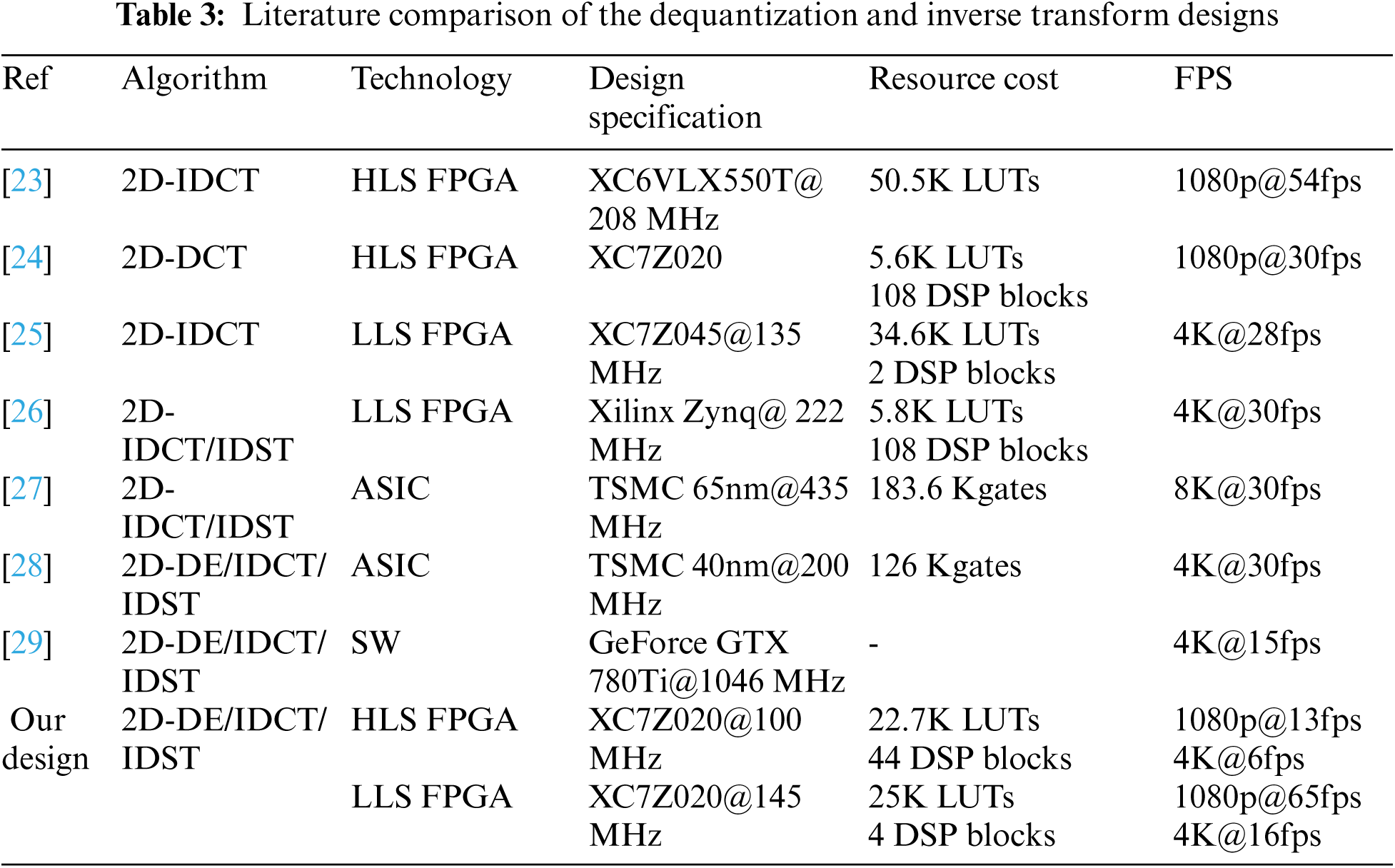
Comparing our HLS 2D-DE/IDCT/IDST design with the HLS design proposed in [23] and [24] used to implement only the 2D-IDCT and 2D-DCT, respectively, we can constate from Tab. 3 that our design allows a gain in LUTs and DSP blocks reaching approximately 55% and 59% relative to [23] and [24], respectively. Moreover, the maximal throughput of our design could perform the decoding of 1080p@13fps at 100 MHz instead of the 1080p@54fps at 208 MHz and 1080p@30fps found in [23] for 2D-IDCT and [24] 2D-DCT only, respectively. On the other hand, the designs [25] and [26] propose the LLS design for the 2D-DCT and 2D-IDCT/IDST only which can achieve 4K@28fps and 4K@30fps, respectively. But, our proposed LLS 2D-DE/IDCT/IDST design can reach 1080p@65fps. Hence, our design has better performance than [25] and [26] in term of frame rate and also use lower LUTs and DSP blocks count than [25] and [26] by 28% and 96%, respectively, as reported in Tab. 3. Further, comparing the LLS 2D-DE/IDCT/DST design with [21], we can constate that our design can process 4K@16fps at 145 MHz instead of 4K@15fps on GeForce GTX 780Ti@1046 MHz in [29]. So, our design is more performant and can achieves lower power consumption. Besides, our design permits more flexibility than [27] and [28] with the almost same performance.
In this work, a unified hardware architecture is proposed to implement the HEVC 2D-DE/IDCT/IDST module for 4/8/16/32 TU block size. However, two design methods are used to design this hardware architecture which are the HLS and the LLS design flow. Our goal was to compare these two methods and to select the best architecture to implement the HEVC 2D-DE/IDCT/IDST module. It is clear from experimental results under Xilinx XC7Z020 FPGA that the LLS design is more performant than HLS design in terms of processing time and hardware cost. But, the performance of HLS design depends on the selected directives, and the algorithm complexity and can be a good solution to speed up the design time and time to market (TTM).
Funding Statement: This work was funded by the Deanship of Scientific Research at Jouf University (Kingdom of Saudi Arabia) under grant No. DSR-2021-02-0391.
Conflicts of Interest: The authors declare that they have no conflicts of interest to report regarding the present study.
1. B. Markwalter, “ATSC 3.0 begins commercial broadcasting: First IP based ultrahigh-definition TV broadcasts on the air,” IEEE Consumer Electronics Magazine, vol. 7, no. 1, pp. 125–126, 2018. [Google Scholar]
2. K. Wiens and P. Corcoran, “Repairability smackdown II: iPhone versus iPhone,” IEEE Consumer Electronics Magazine, vol. 3, no. 1, pp. 19–24, 2014. [Google Scholar]
3. S. Kaur, “The revolution of tablet computers and apps: A look at emerging trends,” IEEE Consumer Electronics Magazine, vol. 2, no. 1, pp. 36–41, 2013. [Google Scholar]
4. G. J. Sullivan, J. Ohm, W. Han and T. Wiegand, “Overview of the high efficiency video coding (HEVC) standard,” IEEE Transactions on Circuits and Systems for Video Technology, vol. 22, no. 12, pp. 1649–1668, 2012. [Google Scholar]
5. K. Glasman, “CE society TV: High efficiency video coding (HEVC),” IEEE Consumer Electronics Magazine, vol. 6, no. 1, pp. 19–22, 2017. [Google Scholar]
6. T. Wiegand, G. J. Sullivan, G. Bjontegaard and A. Luthra, “Overview of the H.264/AVC video coding standard,” IEEE Transactions on Circuits and Systems for Video Technology, vol. 13, no. 7, pp. 560–576, 2003. [Google Scholar]
7. F. Bossen, B. Bross, K. Suhring and D. Flynn, “HEVC complexity and implementation analysis,” IEEE Transactions on Circuits and Systems for Video Technology, vol. 22, no. 12, pp. 1685–1696, 2012. [Google Scholar]
8. M. Kammoun, A. Ben Atitallah, R. Ben Atitallah and N. Masmoudi, “Design exploration of efficient implementation on SoC heterogeneous platform: HEVC intra prediction application,” International Journal of Circuit Theory and Applications, vol. 45, no. 12, pp. 2243–2259, 2017. [Google Scholar]
9. A. Ben Atitallah, H. Loukil, P. Kadionik and N. Masmoudi, “Advanced design of TQ/IQT component for H.264/AVC based on SoPC validation,” WESAS Transactions on Circuits and Systems, vol. 11, no. 7, pp. 211–223, 2012. [Google Scholar]
10. M. Zhang, J. Qu and H. Bai, “Entropy-based fast largest coding unit partition algorithm in high-efficiency video coding,” Entropy, vol. 15, no. 6, pp. 2277–2287, 2013. [Google Scholar]
11. D. Coelho, R. Cintra, F. Bayer, S. Kulasekera, A. Madanayake et al., “Low-complexity loeffler DCT approximations for image and video coding,” Journal of Low Power Electronics and Applications, vol. 8, no. 46, pp. 1–26, 2018. [Google Scholar]
12. A. Ben Atitallah, P. Kadionik, F. Ghozzi, P. Nouel, N. Masmoudi et al., “Optimization and implementation on FPGA of the DCT/IDCT algorithm,” in Proc. IEEE ICASSP, Toulouse, France, 2006. [Google Scholar]
13. A. Ben Atitallah and M. Kammoun, “High-level design of HEVC intra prediction algorithm,” in Proc. ATSIP, Sousse, Tunisia, 2020. [Google Scholar]
14. S. Vivienne and D. Marpe, “Entropy coding in HEVC,” High Efficiency Video Coding (HEVC), Cham, Switzerland: Springer, pp. 209–274, 2014. [Google Scholar]
15. A. Ben Atitallah, P. Kadionik, F. Ghozzi, P. Nouel, N. Masmoudi et al., “HW/SW codesign of the H.263 video coder,” in Proc. IEEE CCECE, Ottawa, ON, Canada, 2006. [Google Scholar]
16. A. B. Atitallah, H. Loukil and N. Masmoudi, “FPGA design for H.264/AVC encoder,” International Journal of Computer Science, Engineering and Applications, vol. 1, no. 5, pp. 119–138, 2011. [Google Scholar]
17. A. Ben Atitallah, I. Abid, A. Boudabous and H. Loukil, “A new hardware architecture of the adaptive vector median filter and validation in a hardware/software environment,” International Journal of Circuit Theory and Applications, vol. 49, no. 8, pp. 2329–2347, 2021. [Google Scholar]
18. M. Kthiri, B. Le Gal, P. Kadionik and A. Ben Atitallah, “A very high throughput deblocking filter for H.264/AVC,” Journal of Signal Processing Systems, vol. 73, no. 2, pp. 189–199, 2013. [Google Scholar]
19. A. Ben Atitallah, A. Boudabous, L. Khriji and N. Masmoudi, “Reconfigurable architecture of VDF filter for multidimensional data,” International Journal of Circuit Theory and Applications, vol. 41, no. 10, pp. 1047–1058, 2013. [Google Scholar]
20. S. Lahti, P. Sjövall, J. Vanne and T. D. Hämäläinen, “Are we there yet? a study on the state of high-level synthesis,” IEEE Transactions on Computer-Aided Design of Integrated Circuits and Systems, vol. 38, no. 5, pp. 898–911, 2019. [Google Scholar]
21. A. Ben Atitallah and M. Kammoun, “High-level design of HEVC intra prediction algorithm,” in Proc. IEEE ATSIP, Sousse, Tunisia, 2020. [Google Scholar]
22. T. M. Alanazi, A. Ben Atitallah and I. Abid, “An optimized SW/HW AVMF design based on high-level synthesis flow for color images,” CMC-Computers Materials & Continua, vol. 68, no. 3, pp. 2925–2943, 2021. [Google Scholar]
23. E. Kalali and I. Hamzaoglu, “FPGA implementations of HEVC inverse DCT using high-level synthesis,” in Proc. DASIP, Krakow, Poland, 2015. [Google Scholar]
24. B. Mohamed, A. Elsayed, O. Amin, E. Khafagy, M. Abdelrasoul et al., “High-level synthesis hardware implementation and verification of HEVC DCT on SoC-FPGA,” in Proc. ICENCO, Cairo, Egypt, 2017. [Google Scholar]
25. M. Kammoun, E. Maamouri, A. Ben Atitallah and N. Masmoudi, “An optimized hardware architecture of 4 × 4, 8 × 8, 16 × 16 and 32 × 32 inverse transform for HEVC,” in Proc. IEEE ATSIP, Monastir, Tunisia, 2016. [Google Scholar]
26. M. Chen, Y. Zhang and L. Chao, “Efficient architecture of variable size HEVC 2D-DCT for FPGA platforms,” International Journal of Electronics and Communications, vol. 73, pp. 1–8, 2017. [Google Scholar]
27. H. Liang, W. He, G. He and Z. Mao, “Area-efficient HEVC IDCT/IDST architecture for 8kx4k video decoding,” in Proc. IEICE Electron Express, 2016. [Google Scholar]
28. M. Tikekar, C. -T. Huang, V. Sze and A. Chandrakasan, “Energy and area-efficient hardware implementation of HEVC inverse transform and dequantization,” in Proc. IEEE ICIP, Paris, France, 2014. [Google Scholar]
29. D. F. De Souza, N. Roma and L. Sousa, “Opencl parallelization of the HEVC de-quantization and inverse transform for heterogeneous platforms,” in Proc. IEEE EUSIPCO, Lisbon, Portugal, 2014. [Google Scholar]
30. W. H. Chen, C. H. Smith and S. C. Fralick, “A fast computational algorithm for the discrete cosine transform,” IEEE Transactions on Communications, vol. 25, no. 9, pp. 1004–1009, 1977. [Google Scholar]
31. C. Rosewarne, Joint Collaborative Team on Video Coding (JCT-VC) (2017) High efficiency video coding (HEVC) test model 16 (HM 16). [Google Scholar]
 | This work is licensed under a Creative Commons Attribution 4.0 International License, which permits unrestricted use, distribution, and reproduction in any medium, provided the original work is properly cited. |