DOI:10.32604/cmc.2022.024004
| Computers, Materials & Continua DOI:10.32604/cmc.2022.024004 | |
| Article |
Fuzzy System Design Using Current Amplifier for 20 nm CMOS Technology
1Jaypee University of Information Technology, Waknaghat, 172234, India
2Symbiosis Institute of Technology, Symbiosis International (Deemed University), Pune, 411021, India
3School of Computer Science and Engineering, The University of New South Wales, Sydney, NSW 2052, Australia
4Symbiosis Centre for Applied Artificial Intelligence, Symbiosis International (Deemed University), Pune, 411021, India
*Corresponding Author: Ketan Kotecha. Email: head@scaai.siu.edu.in
Received: 30 September 2021; Accepted: 12 January 2022
Abstract: In the recent decade, different researchers have performed hardware implementation for different applications covering various areas of experts. In this research paper, a novel analog design and implementation of different steps of fuzzy systems with current differencing buffered amplifier (CDBA) are proposed with a compact structure that can be used in many signal processing applications. The proposed circuits are capable of wide input current range, simple structure, and are highly linear. Different electrical parameters were compared for the proposed fuzzy system when using different membership functions. The novelty of this paper lies in the electronic implementation of different steps for realizing a fuzzy system using current amplifiers. When the power supply voltage of CDBA is 2 V, it results in 155 mW, power dissipation; 4.615 KΩ, input resistance; 366 KΩ, output resistances; and 189.09 dB, common-mode rejection ratio. A 155.519 dB, voltage gain, and 0.76 V/μs, the slew rate is analyzed when the power supply voltage of CDBA is 3 V. The fuzzy system is realized in 20 nm CMOS technology and investigated with an output signal of high precision and high speed, illustrating that it is suitable for real-time applications. In this research paper, a consequence of feedback resistance on the adder circuit and the defuzzified circuit is also analyzed and the best results are obtained using 100 K resistance. The structure has a low hardware complexity leading to a low delay and a rather high quality.
Keywords: Current amplifiers; membership functions; fuzzy system; fuzzy operators; defuzzified circuit; feedback resistance
Circuits produce output based upon input stimulus. There are advantaged crossover points in both circuit types where one approach is better than another. The crossover points are based on the composite requirements of precision, speed, noise, power, physical size, and cost. In 1965, Gordon Moore realized a striking trend for the growth in memory chip performance. Each new memory chip comprises approximately twice the capacity of its precursor. Every chip was realized in 18–24 months of the preceding chip. He observed that if this trend remains then computing power can rise exponentially in a small time. The increase in trend towards low power systems and high performance leads to innovative design methodology [1]. This helps in meeting the stringent system requirements and many of them are performing stream data processing. Many of the processes in image/signal processing have complex, or nonstationary signals/images which are difficult to model and significantly influenced by immense parameters [2]. Thus, precise models of the system become inconvenient to produce output as operation complication increases. This is, nevertheless, sometimes impractical in signal processing, since precise models are needed to provide better systems. Complex circuits are not easy to design. It requires special design or methodologies. To overcome this problem Integrated Circuits (IC) technology helps in producing chips using a different number of transistors. An IC design imparts challenges in choosing the circuit topology and size due to the presence of active devices. Every active device has different electrical characteristics. The flexibility for the design of the circuit is high. Despite the flexibility, there are some limitations of one level of the design to compensate for the shortcomings at higher levels. These limitations occur due to inherent constraints in the technology specifying speed, power, performance, throughput, complexity, etc. Performance is an issue that is addressed at all levels of the design. The optimized and design decisions are more important at higher levels than that at low levels. The system design and Very Large-Scale Integration (VLSI) circuit processes are similar to the traditional software design. The VLSI technology development, with completely integrated systems or never decreasing demand for substantial analog circuits and number of digital circuits on one chip [3]. In general, analog is best when input stimulus signals are small and/or continuously variable (i.e., a microphone), or output load power requirements are high (i.e., a 150 W off-line power supply). The digital circuits are best in the middle between the analog input and output circuits (i.e., filtering and waveshaping via digital signal processing). With the invention of IC, the operational amplifier (op-amp) has functioned as the building block in analog circuit design [4]. In the area of analog signal processing, a significant quantity of literature has been dedicated to the awareness of a selection of active devices. The future may mostly be digital but wide swaths of technology will always be analog. A new idea in this field helps to give further improvements to get more engrossing and efficacious circuits. There are numerous novel active elements established out of which numerous of them are just theoretical components that offer further research.
There are different modes of operations like voltage mode (VM), trans resistance mode, current mode (CM), or transconductance mode. Analog circuits like sinusoidal oscillators, voltage comparators, converters, amplifiers, etc. are circuits that cannot be used by any other digital techniques [3,4]. Analog circuit design is a voltage-controlled form of signal processing and guaranteed that the circuits should be compatible with the CMOS technology. The voltage feedback operational amplifier is one of the direct-coupled high gain voltage amplifiers that help in the amplification of ac/dc input voltage [5]. During the last few decades, CM processing has emerged as a viable alternative over VM processing due to its inherent advantages like wider bandwidth, greater linearity, larger dynamic range, higher bandwidth, high slew rate, and better signal linearity. The −3 dB bandwidth of the current amplifier is independent of closed-loop gain, because of using negative feedback [6]. The circuits are designed for lower voltage swings; due to this reason small voltage supplies are used. Current amplifiers have theoretically infinite output impedance, and a rated load must always be connected. They will always drive an output current that is proportional to the input voltage. Frequently they are used in DC power supplies. The output current is sensed by a shunt or a generously rated heat sink-resistor which creates a voltage that is feedback to the input circuit. The regulation of a current amplifier can be calculated by shorting out the output terminals and measuring the drop in current a few percent. Advancements in current mode processing have led to the materialization of new analog building blocks. In addition to the preferment in CM signal processing, new current-mode analog building blocks are developed. In practical cases, the output load impedance is allowed to change within a range of values [6]. The current amplifier is a power amplifier that has zero input impedance and an ideally (dynamically) infinite out impedance [7]. In contrast, a voltage amplifier has zero output impedance and infinite input impedance, and it produces an output voltage that is proportional to the input voltage. Current amplifiers have theoretically infinite output impedance, and a rated load must always be connected. They will always drive an output current that is proportional to the input voltage. Frequently they are used in DC power supplies [8,9]. The output current is sensed by a shunt or a generously-rated heatsink-resistor which creates a voltage that is feedback to the input circuit. The regulation of a current amplifier can be calculated by shorting out the output terminals and measuring the drop in current–a few percent [10]. The different current amplifiers are current-feedback operational amplifiers (CFOA), two-stage CMOS operational amplifiers (2SCOA) [11,12], current conveyors (CCII), operational transconductance amplifiers (OTA) [13,14], current differencing buffered amplifier (CDBA) [15–18], and current differencing transconductance amplifier (CDTA) [19]. This research paper mainly deals with the designing of different circuits used in designing a Fuzzy system using CDBA. CDBA is simple in implementation, has a high slew rate, no parasitic capacitance, and wide bandwidth [20]. Different applications found on CDBA are reported in the literature namely CM filters [21], VM filters [22–24], oscillators [25–28], fully integrated gyrator circuits. Due to unity gain voltage amplifier and current differencing, the CDBA is a flexible active building block that helps in signal processing applications.
The concept of fuzzy logic was introduced by Zadeh (1968) that explains the human reasoning model considering numerous rules to varying degrees of membership. Fuzzy logic is inspired by two objectives [29–31]. First, it focuses to reduce problems in analyzing and developing intricate systems experienced by traditional mathematical tools, and another is inspired by monitoring human motivation that utilizes knowledge and concepts which are not well defined and have tapered limitations. The first motive is linked to solving real-world problems and requires fuzzy logic to effort in numeric & quantitative domains. While the second motivation is related to Artificial Intelligence (AI) to have a qualitative and descriptive form. These two motivations make fuzzy logic unique and different from other techniques [31]. The fuzzy system consists of five main steps [32]. In fuzzification inputs are defined and each input is assigned with linguistic variables (low, medium, high) and every linguistic variable is assigned with different membership functions (MF) like S, Z, triangular, pi, Gaussian, etc. [33]. The shape of each MF is similar to the name. Fuzzy operators are used to making rules using the IF-ELSE statement. Combining all the rules is known as aggregation and finally, the defuzzification process is implemented to get crisp (one) value. For the evaluation of the fuzzy system, different electrical parameters are calculated [32,33].
The op-amp-based circuits depict numerous disadvantages in their accomplishment like limited bandwidth and slew-rate. Therefore, the current-mode method has been considered in this research work as a means to conquer the op-amp stumbling block and to perceive high-speed systems. In this paper, a novel analog design and implementation of different steps of fuzzy systems using CDBA are presented with a compact structure that can be used in many signal processing applications. Different electrical parameters were compared for the proposed fuzzy system when using different membership functions. The effect of supply voltages and feedback resistance on the proposed fuzzy system was analyzed. The novelty of this paper lies in the electronic implementation of different steps for realizing a fuzzy system using current amplifiers. The authors are unable to do the simulations below 2 V and above 5 V. The Fuzzy system was realized in 20 nm CMOS technology and investigated with an output signal of high precision and high speed, illustrating that it is appropriate for real-time applications.
This paper is divided as Section 2 explains materials and methodology for the designing of a fuzzy system for various power supply voltages of CDBA. The results were compared with different current amplifiers. Section 3 illustrates the results and discussion which was concluded in the last section.
An operational amplifier is the principal building block for the implementation of analog signal circuits or different image processing circuits. The bandwidth of the operational amplifier is reliant on closed-loop voltage gain. To conquer this difficulty, current mode circuits are preferred [23]. In this paper, a novel analog design and implementation of different steps of fuzzy systems using CDBA are presented with a compact structure that can be used in many signal processing applications. The implementation steps for designing the fuzzy system are shown in Fig. 1.
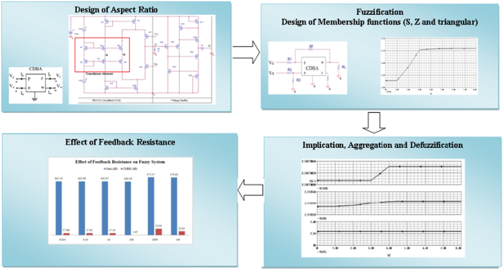
Figure 1: Proposed methodology for designing of fuzzy system using CDBA
The current feedback operational amplifier (CFOA) (AD-844) [34] has high-speed, high slew rate, and high gain-bandwidth that can be used for low/medium frequency applications [35,36]. The CFOA is a four-terminal device while the voltage operational amplifier is a three-terminal device. Acar et al. [15] proposed an analog component utilizing two inputs (ip and in) and two outputs (iz and iw) as a current difference buffered amplifier (CDBA) which is designed using CFOA as shown in Fig. 2.
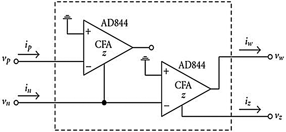
Figure 2: Design of CDBA using CFOA [35]
In Fig. 2, n and p are the negative & positive current input terminals respectively. Z and w are the current and voltage output terminal. Due to this reason, CDBA can work in current and voltage mode. This enables the different circuit designs. The voltage and current equations are explained using Eq. (1).
The characteristics equation of CDBA is given by Eqs. (2)–(4).
As per Eq. (2), the output current (Iz) is the difference between the two input terminus currents. Eq. (4) explains that the voltage at terminus w is equal to the voltage at z terminus. CDBA is also known as the cascade relation of the current subtractor and a voltage follower.
2.1 Execution of CDBA Using Different MOSFETs
CDBA is considered as a distinctive type of current feedback amplifier with grounded y input and differential current input. The input impedance at the terminus n and p is ideally zero because the input currents In and Ip are internally grounded. The CDBA can be used for high-frequency performance and are free from parasitic capacitances. CDBA is used by many researchers for designing different analog signal processing circuits. CDBA comprises of two circuits namely Differential Current Controlled Current Source (DCCCS) and a voltage buffer. DCCCS consists of finite input resistance. The internal diagram of CDBA is displayed in Fig. 3.
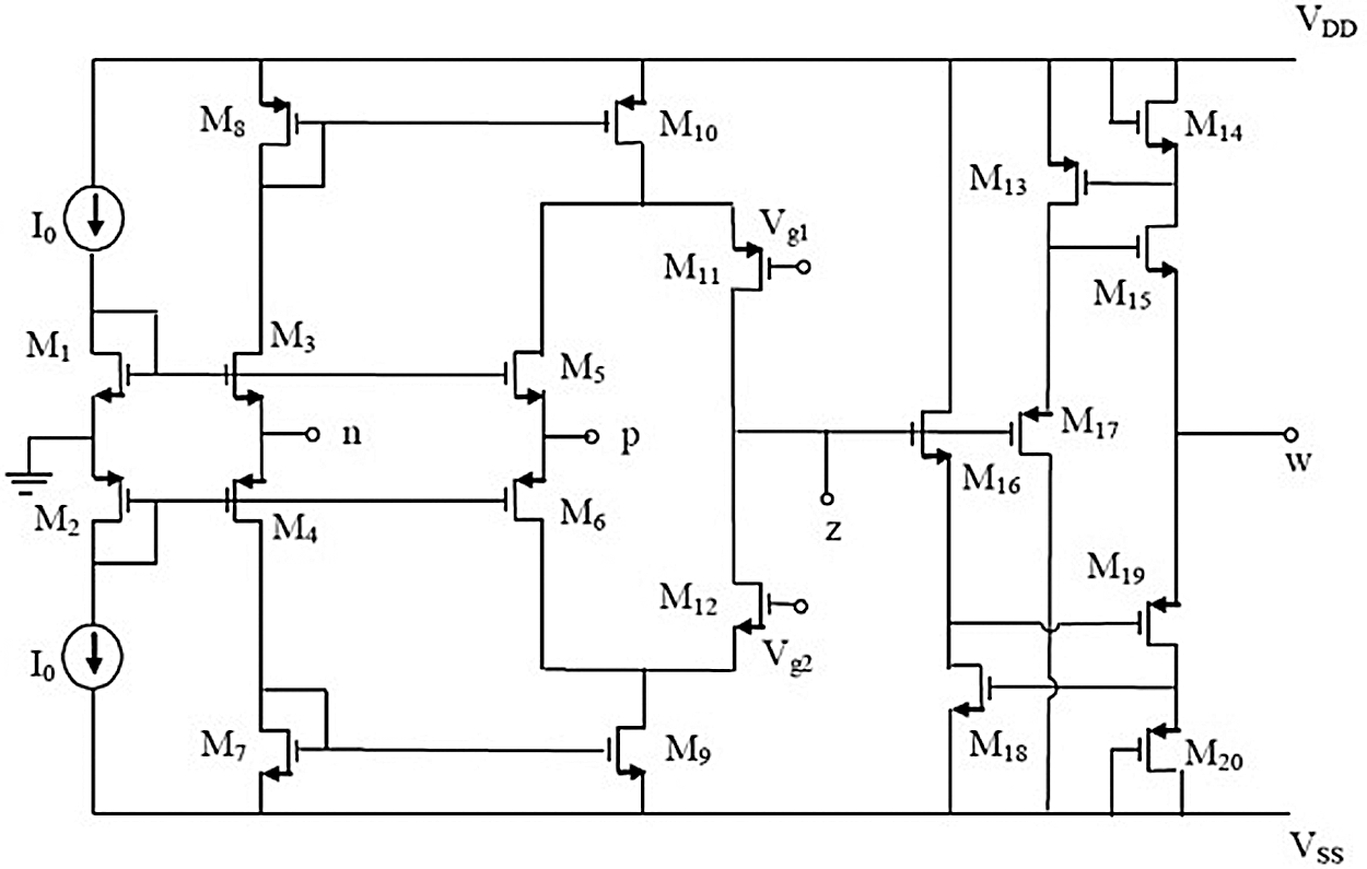
Figure 3: Execution of CDBA using different MOSFETs
2.2 Design Steps of Calculation of Aspect Ratio of Different MOSFET's
For any design appropriate (W/L) sizing of the circuit element should be considered. The problem is related to the finding of optimal length and width values of different MOSFETs. For designing CDBA circuit, W and L values of each MOSFET has been calculated by considering the following physical parameters : GB = 5 MHz, VDD = −VSS = 2.5 V, k`P = 50 μA/V2, k`N = 110 μA/V2, VTN = 0.7 ± 0.15 V, VTP = −0.7 ± 0.15 V, λP = 0.05 V−1, λN = 0.04 V−1, SR > 10 V/μs, CL = 10 PF, GAIN > 5000 V/V, −1.5 V < ICMR < 2.5 V, PDIS < 1 MW, VT0 (max) = 0.85 V, VT0 (min) = 0.55 V, Vin(max) = 2 V, Vin(min) = 1 V, VTI (max) = 0.85 V. For calculating (W/L)3 and (W/L)4, Eq. (5) is used.
For Eq. (5), the current is calculated by using, Eq. (6)
where CC > 0.22 CL = 2.2 pF
Putting values of SR and Cc in Eq. (6) we get I
Putting all values in Eq. (5), values of (W/L)3 and (W/L)4 is calculated as
For calculating (W/L)13 and (W/L)14, Eq. (8) is used.
In Eq. (8), gm1 is calculated by using Eq. (9)
Assuming CC = 3 pF, gm1 is analysed as
Placing values in Eq. (8) values of (W/L)13 and (W/L)14 is evaluated as :
(W/L)1, (W/L)2, (W/L)6, (W/L)8, (W/L)10 is also equal to (W/L)13.
For calculation of (W/L), 15 Eq. (11) is used
In Eq. (11), initially, VDS15 sat has to be calculated this is analyzed by Eq. (12).
Putting physical parameter values in Eq. (12), VDS15 sat is calculated as 0.35 V and placing this value in. Eq. (11), (W/L)15 is analyzed as
Considering all the positive aspects of CDBA, in this paper different membership functions, fuzzy operators, adder circuits, and defuzzified circuits were designed and simulated using CDBA [35–38] in SPICE software. The comparison has been done considering various current amplifiers based on different electrical parameters. The comparison of different electrical parameters was evaluated based on various power supply voltages for one membership function and later in the combination of different membership functions were analyzed. Lastly, the effect of feedback resistance (RF) was also evaluated on the designed adder and de-fuzzified circuit. All the simulations were carried out using SPICE software [39–41] in Intel Core i3-2120 CPU @ 3.30 processor, 4 GB RAM.
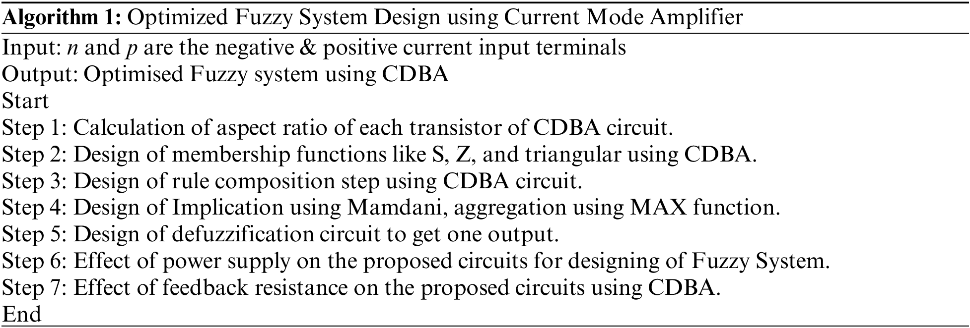
As the requirement for mixed-mode integrated circuits rises, the design of analog circuits’ like op-amps using CMOS technology turns out to be more analytical. In this research paper, the authors have suggested a new system for deciding the aspect ratio and transistor dimensions for current-mode CMOS op-amps. The proposed model is explained using Algorithm 1.
The technique holds a broad variation of constraints and specifications, exceptionally fast, and consequence in optimal outlines. The performance of the op-amp is evaluated using different electrical parameters. In this paper, the CMOS amplifier design problem is considered for determining the different design parameters. This design issue can be approximated in various ways, like computer-aided design methods.
3.1 Design of Membership Functions
The main aim is to design and simulate S, Z, and triangular MF's using CDBA.
Sigma (S) MF: The concept of implementing S MF by CDBA is the same as used for implementing op-amp [33]. Fig. 4 exhibits the block diagram of the implementation of the S function where the two inputs to the amplifier are shown as variable crisp input (Vx ) and constant input voltage (Vc.). In this paper, S MF is designed for gain 2 for VC as 1 V and VX as 3 V (assuming saturation voltage 4 V) [9,14].
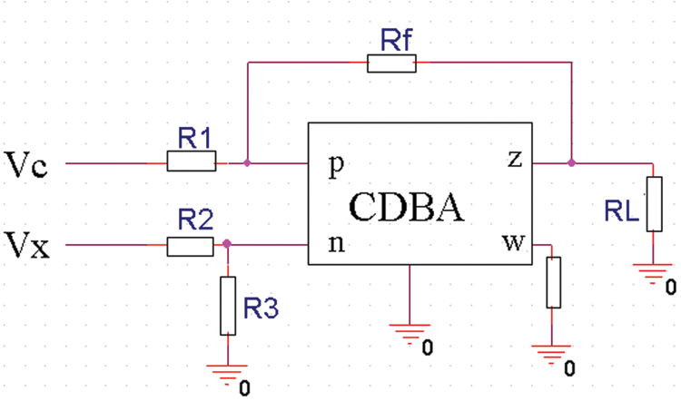
Figure 4: Design of S MF
Anti Sigma (Z) Membership function: The Z MF output is an inversion of the output of S MF. Fig. 5, displays the block diagram of the Z function. In this paper, Z MF is designed to gain 4 and by considering VC : 1 V, saturation voltage as 4 V, and VX as 2 V [9].
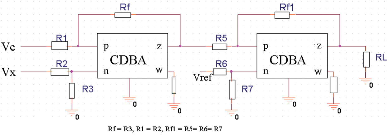
Figure 5: Design of Z MF
Triangular MF: The triangular MF is a combination of S and Z MF. Zadeh Berkeley et al. [33] show the designing of triangular MF.
In this paper, the authors have discussed the effect of feedback and resistance. Figs. 6–8 show the output of triangular MF using RF = 0.0001, 0.001, and 0.01 K respectively.
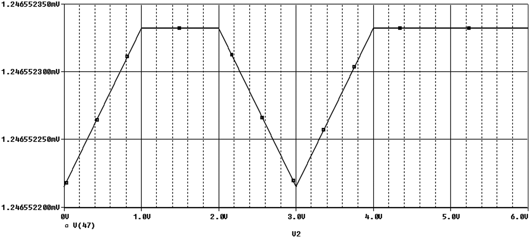
Figure 6: Triangular MF using RF 0.0001 K
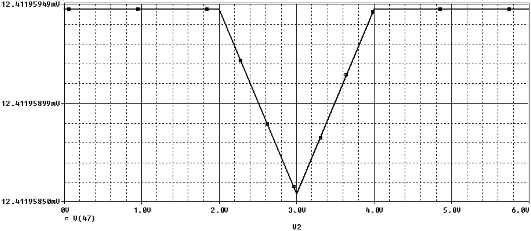
Figure 7: Triangular MF using RF 0.001 K
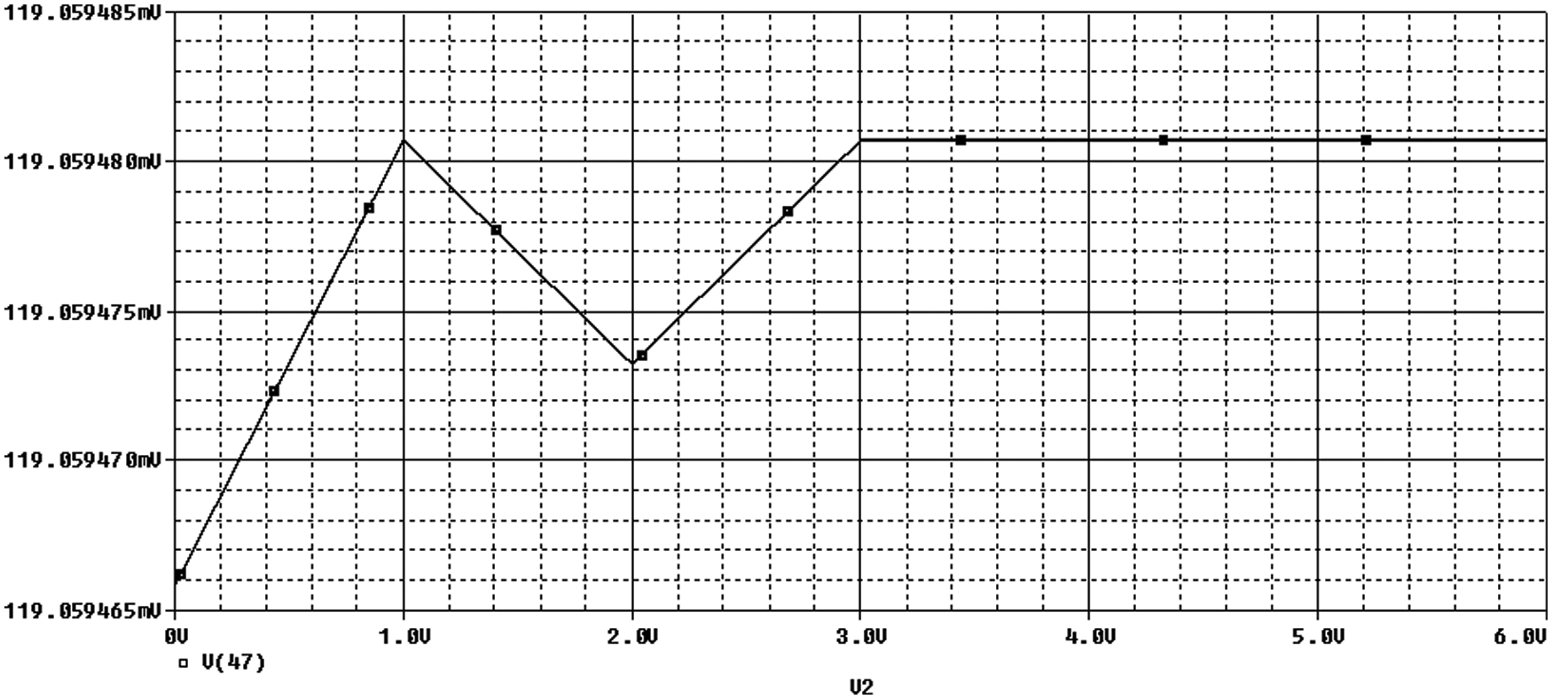
Figure 8: Triangular MF using RF 0.01 K
For any circuit, the loading effect can be reduced by keeping input impedance high and output impedance low. To raise the speed of the circuit, CMRR and slew rate should be high, but power dissipation should be low.
3.2 Implementation of Fuzzy System
The linguistic variables with different membership functions were defined for every input and output. Rules were made for input/output (rule composition and implication). All the rules were aggregated and finally, defuzzified output is obtained. The circuits for rule composition, fuzzy operators, and defuzzified circuits were implemented and the final result is shown in Fig. 9. It shows the result of designed aeration and defuzzified circuit output designed using CDBA with the same reference voltage and power supply voltage of 2 V. In Fig. 9, V(63) and V(65) are the aggregated and defuzzified circuit output respectively.
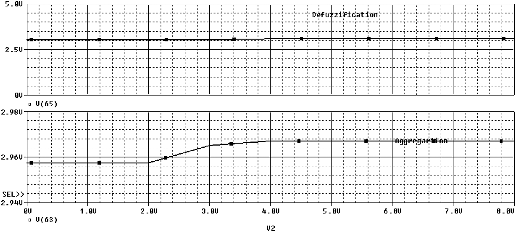
Figure 9: Final output of the fuzzy system using 2 V
The effect of power supply and feedback resistance is studied for the proposed circuits for designing the fuzzy system.
3.2.1 Effect of Power Supply on the Proposed Circuits for Designing of Fuzzy System Using CDBA
The various electrical parameters of fuzzy systems using CDBA are evaluated & comparison is done with other current and voltage amplifiers (operational amplifier (op-amp), 2SCOA, and OTA). Tab. 1 shows the comparison of electrical parameters for S MF using various power supply voltages of different current amplifiers and Tab. 2 tabulates the comparison table of different electrical parameters for S and Z MF using a variable power supply voltage of different current amplifiers.
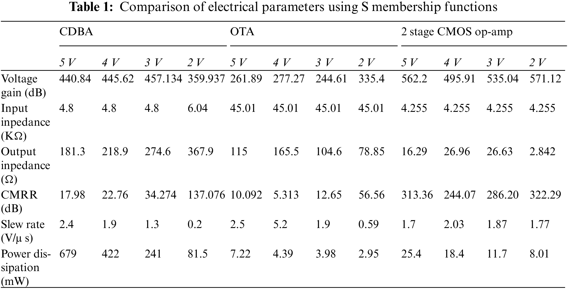
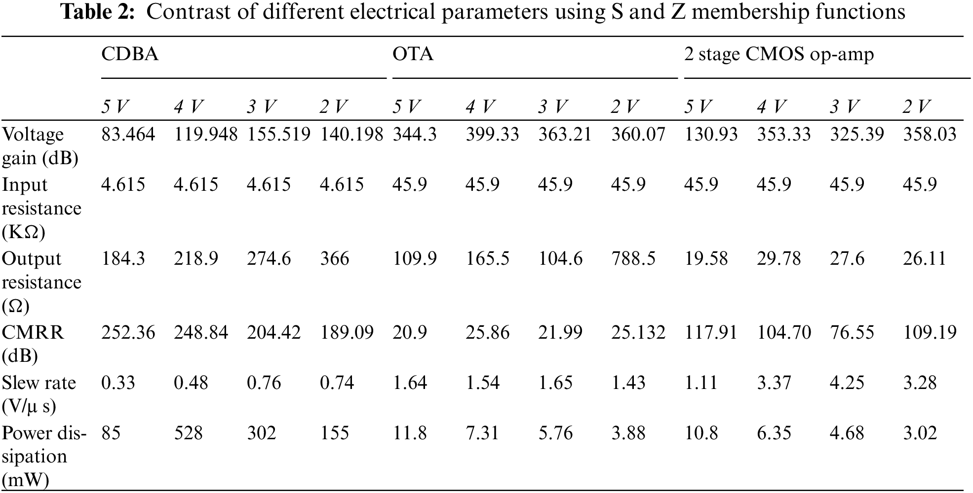
The power dissipation of 155 mW, the input resistance of 4.615 KΩ, the output resistance of 366 KΩ, CMRR of 189.09 dB for different membership functions, and the same power supply voltage of CDBA & reference voltage of 2 V shows the remarkable results. The voltage gain of 155.519 dB and slew rate of 0.76 V/μs is obtained when 3 V is used.
3.2.2 Effect of Feedback Resistance on the Proposed Circuits for the Designing of the Fuzzy System Using CDBA
Figs. 10a–10d shows the effect of feedback resistance (values from 1, 10, 100 K, 1 M) on the proposed circuit using CDBA. V(168), V(68), and V(63) show the implication, aggregation, and defuzzified output respectively. Results with 100 K show remarkable performance as its CMRR and voltage gain is high. A comparison of the effect of feedback resistance on CMRR and voltage gain is depicted in Fig. 11.
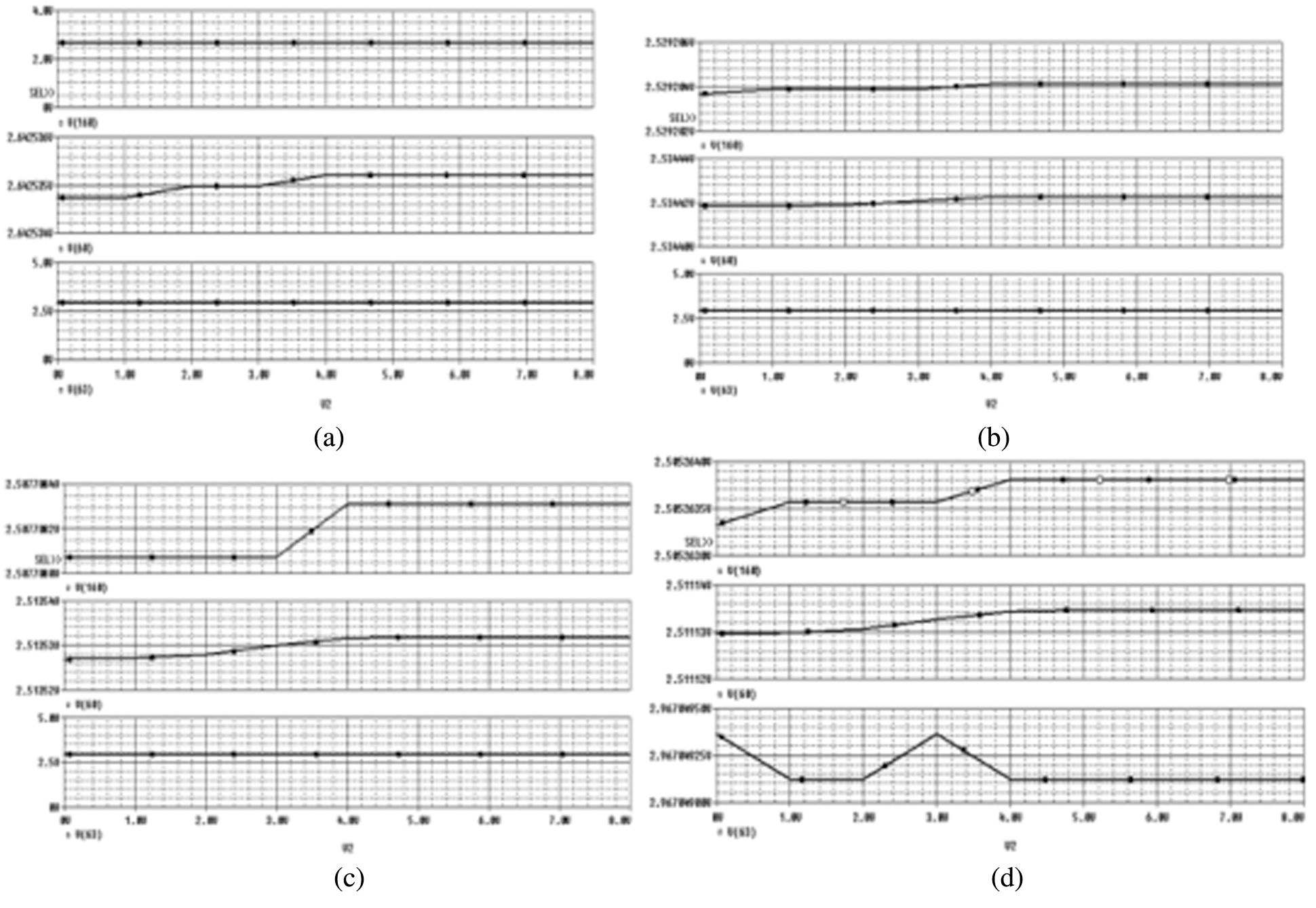
Figure 10: Effect of feedback with (a) 1 K resistance (b) 10 K resistance (c) 100 K resistance (d)1 M resistance
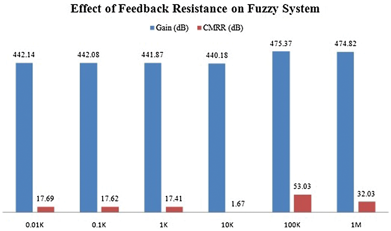
Figure 11: Effect of feedback resistance on the design of the de-fuzzified circuit
To authenticate the theoretical analysis, all the recommended circuits have been imitated using the PSPICE program. Theoretical analysis and simulation results were verified by experimental testing. A novel analog fuzzy system is designed and implemented using CDBA that can be used in many signal processing applications.
This paper focused on hardware taxonomy and highlights the attributes of the distinct applications covering the afore-mentioned paradigms covered over the last two decades and the source of the current decade. Therefore, the current-mode approach has been considered in this research work as a way to overcome the op-amp stumbling block and to perceive high-speed systems. In this paper, a novel analog design and implementation of different steps of fuzzy systems using CDBA are presented with a compact structure that can be used in many signal processing applications. Different electrical parameters were compared for the proposed fuzzy system when using different membership functions. The effect of feedback resistance was also analyzed on the designed circuits for the fuzzy system. The results of this research give strong motivation for the IC design of CDBA, a current-mode analog signal processing circuit. The simulation results are found in close agreement with the theoretical results. The Fuzzy system was investigated with an output signal of high precision and high speed, illustrating that it is suitable for real-time applications.
Funding Statement: This work was supported by Research Support Fund (RSF) of Symbiosis International (Deemed University), Pune, India.
Conflicts of Interest: The authors declare that they have no conflicts of interest to report regarding the present study.
1. D. Biolek, R. Senani, V. Biolkova and Z. Kolka, “Active elements for analog signal processing: Classification, review and new proposals,” Radio Engineering, vol. 17, pp. 15–32, 2008. [Google Scholar]
2. P. E. Allen and D. R. Holberg, “CMOS analog circuit design,” International Student Edition, New York, USA: Oxford, pp. 22–39, 2011. [Google Scholar]
3. E. S. Sinencio and J. S. Martinez, “CMOS transconductance amplifiers, architectures and active filters: A tutorial,” in IEEE Proc. on Circuits Devices System, Cancun, Mexico, vol. 147, pp. 3–12, 2000. [Google Scholar]
4. R. Sarma, C. Bhargava, S. Jain and V. K. Kamboj, “Application of ameliorated harris hawks optimizer for designing of low-power signed floating-point MAC architecture,” Neural Computing and Applications, vol. 16, pp. 1–30, 2021. [Google Scholar]
5. R. Sarma, C. Bhargava, S. Dhariwal and S. Jain, “UCM: A novel approach for delay optimization,” International Journal of Performability Engineering, vol. 15, pp. 1190–1203, 2019. [Google Scholar]
6. A. Toker, S. Ozoguz, O. Cicekoglu and C. Acar, “Current-mode all-pass filters using current differencing buffered amplifier and a new high-bandpass filter configuration,” IEEE Transactions on Circuits and Systems-II; Analog and Digital Signal Processing, vol. 47, no. 9, pp. 949–954, 2000. [Google Scholar]
7. R. A. Gayakwad, Op-amps and Linear Integrated Circuits, 3rd ed., New Delhi, India: PHI, pp. 97–122, 2001. [Google Scholar]
8. H. Upadhyay, S. Juneja, A. Juneja, G. Dhiman and S. Kautish, “Evaluation of ergonomics-related disorders in online education using fuzzy AHP,” Computational Intelligence and Neuroscience, vol. 2021, pp. 1–11, 2021. [Google Scholar]
9. S. Ozoguz, A. Toker and C. Acar, “Current-mode continuous-time fully integrated universal filter using CDBAs,” Electronics Letters, vol. 35, pp. 97–98, 1999. [Google Scholar]
10. S. Jain, “Design and simulation of fuzzy system using two stage CMOS operational amplifier,” Journal of Active and Passive Electronic Devices, vol. 9, no. 4, pp. 1–12, 2014. [Google Scholar]
11. S. Mahalingam, M. A. Mamun, L. F. Rahman and W. M. D. W. Zaki, “Design and analysis of a two stage operational amplifier for high gain and high bandwidth,” Australian Journal of Basic and Applied Sciences, vol. 6, no. 7, pp. 247–254, 2012. [Google Scholar]
12. P. D. Patel and K. A. Shah, “Design of low power two stage CMOS operational amplifier,” International Journal of Science and Research, vol. 2, no. 3, pp. 432–434, 2013. [Google Scholar]
13. S. Jain, “Implementation of fuzzy system using operational transconductance amplifier for ERK pathway of EGF/insulin leading to cell survival/death,” J. Pharm Biomed Sci., vol. 4, no. 8, pp. 701–707, 2014. [Google Scholar]
14. S. Jain, “Design and simulation of fuzzy system using operational transconductance amplifier,” Smart Innovation, Systems and Technologies, vol. 31, pp. 265–273, 2015. [Google Scholar]
15. C. Acar and S. O¨ zoǧuz, “A new versatile building block: Current differencing buffered amplifier suitable for analog signal processing filters,”Microelectronics Journal, vol. 30, no. 2, pp. 157–160, 1999. [Google Scholar]
16. W. Tangsrirat and W. Surakampontorn, “Realization of multiple-output biquadratic filters using current differencing buffered amplifiers,”International Journal of Electronics, vol. 92, no. 6, pp. 313–325, 2005. [Google Scholar]
17. H. Sedef and C. Acar, “On the realization of voltage-mode filters using CDBA,” Frequenz, vol. 54, no. 9–10, pp. 198–202, 2000. [Google Scholar]
18. S. Maheshwari and I. A. Khan, “Novel voltage-mode universal filter using only two CDBAs,” Journal of Circuits, Systems and Computers, vol. 14, no. 1, pp. 159–164, 2005. [Google Scholar]
19. S. Jain, “To design high CMRR, high slew rate instrumentation amplifier using OTA and CDTA for biomedical application,” International Journal of Engineering Research (IJER), vol. 2, pp. 332–336, 2013. [Google Scholar]
20. K. N. Salama and A. M. Soliman, “Voltage mode kerwin-huelsman-newcomb circuit using CDBAs,”Frequenz, vol. 54, no. 7–8, pp. 90–93, 2000. [Google Scholar]
21. S. Özoguz, A. Toker, M. A. İbrahim and C. Acar, “A new versatile building block: Current differencing amplifier and its applications,” in Proc. of the European Conf. on Circuit Theory and Design, ECCTD’99, Stresa, Italy, pp. 90–93, 1999. [Google Scholar]
22. H. Sedef and C. Acar, “On the realization of voltage-mode filters using CDBA,” Frequenz, vol. 54, pp. 198–202, 2000. [Google Scholar]
23. W. Tangsrirat, “Voltage-mode multifunction biquadratic filter and sinusoidal oscillator using only two CDBAs,” Journal of Active and Passive Electronic Devices, vol. 4, no. 4, pp. 335–345, 2009. [Google Scholar]
24. S. Özcan, A. Toker, C. Acar, H. Kuntman and O. Çiçekoğlu, “Single resistance controlled sinusoidal oscillators employing current differencing buffered amplifier,” Microelectronic Journal, vol. 31, pp. 169–174, 2000. [Google Scholar]
25. A. U. Keskin, “Voltage-mode high-Q band-pass filters and oscillators employing single CDBA and minimum number of components,” International Journal on Electronics, vol. 92, no. 8, pp. 479–487, 2005. [Google Scholar]
26. S. Juneja, M. Gahlan, G. Dhiman and S. Kautish, “Futuristic cyber-twin architecture for 6G technology to support internet of everything,” Scientific Programming, vol. 2021, pp. 1–13, 2021. [Google Scholar]
27. S. O¨zoǧuz, A. Toker and C. Acar, “Current-mode continuous time fully-integrated universal filter using CDBAs,” ElectronicsLetters, vol. 35, no. 2, pp. 97–98, 1999. [Google Scholar]
28. A. U. Keskin and E. Hancioglu, “Current mode multifunction filter using two CDBAs,” Internatioanl Journal of Electronics and Communications, vol. 12, pp. 1–9, 2005. [Google Scholar]
29. R. C. Berkan and S. L. Trubatch, Fuzzy System Design Principles, 1st ed., New Jersey, USA: Wiley-IEEE Press, pp. 31–57, 1997. [Google Scholar]
30. D. Drankov., H. Hellendoorn and M. Reinfrank, An Introduction to Fuzzy Control, New York: Springer-Verlag, pp. 87–111, 1993. [Google Scholar]
31. M. Gupta, K. K. Gupta, M. R. Khosravi, P. K. Shukla, S. Kautish et al., “An intelligent session key-based hybrid lightweight image encryption algorithm using logistic-tent map and crossover operator for internet of multimedia things,” Wireless Personal Communications, vol. 121, no. 3, pp. 1–22, 2021. [Google Scholar]
32. J. Yen and R. Langari, Fuzzy Logic: Intelligent Control and Information, 1st edition, USA: Prentice Hall, pp. 21–46, 1998. [Google Scholar]
33. L. A. Zadeh Berkeley and CA January 10, 1995. http://radio.feld.cvut.cz/matlab/toolbox/fuzzy/fuzzytu3.html, last accessed on 25th September, 2021. [Google Scholar]
34. S. Jain and D. S. Chauhan, “Implementation of fuzzy system using different voltages of OTA for JNK pathway leading to cell survival/death,” Network Biology, vol. 5, pp. 62–70, 2015. [Google Scholar]
35. S. Jain, “Design and simulation of fuzzy membership functions for the fuzzification module of fuzzy system using operational amplifier,” International Journal of Systems, Control and Communications (IJSCC), vol. 6, pp. 69–83, 2014. [Google Scholar]
36. W. Tangsrirat, W. Surakampontorn and N. Fujii, “Realization of leapfrog filters using current differencing buffered amplifiers,” IEICE Trans Fundamentals, vol. 86, pp. 318–326, 2003. [Google Scholar]
37. W. Tangsrirat, T. Pukkalanun and W. Surakampontorn, “CDBA-Based universal biquad filter and quadrature oscillator,” Active and Passive Electronic Components, vol. 2008, pp. 1–7, 2008. [Google Scholar]
38. C. Bhargava and G. M. Khanal, Advanced VLSI Technology Technical Questions and Solutions, in 1st ed., Denmark: Rivers Publishers, pp. 27–31, 2020. [Google Scholar]
39. C. Acar and H. Sedef, “Realization of nth-order current transfer function using current differencing buffered amplifiers,” Int. J. Electronics, vol. 90, pp. 277–283, 2003. [Google Scholar]
40. M. A. Nguyen, Pspice Tutorial, Class: Power Electronics, 1st ed., Colorado: Colorado State University, pp. 1–56, 2014. [Google Scholar]
41. M. H. Rashid, Introduction to PSICE Using OrCAD for Circuits and Electronics, 3rd ed., India: PHI, pp. 55–90, 2008. [Google Scholar]
 | This work is licensed under a Creative Commons Attribution 4.0 International License, which permits unrestricted use, distribution, and reproduction in any medium, provided the original work is properly cited. |