DOI:10.32604/cmc.2022.024516
| Computers, Materials & Continua DOI:10.32604/cmc.2022.024516 | |
| Article |
An Evolutionary Normalization Algorithm for Signed Floating-Point Multiply-Accumulate Operation
1Department of Electrical & Electronics Engineering, Faculty of Engineering & Technology, Jain (Deemed-to-be-University), Ramanagar, 562112, Karnataka, India
2Symbiosis Institute of Technology, Symbiosis International (Deemed University), Lavale, Pune, 412115, India
3Symbiosis Centre for Applied Artificial Intelligence, Symbiosis International (Deemed University), Lavale, Pune, 412115, India
*Corresponding Author: Ketan Kotecha. Email: head@scaai.siu.edu.in
Received: 20 October 2021; Accepted: 22 December 2021
Abstract: In the era of digital signal processing, like graphics and computation systems, multiplication-accumulation is one of the prime operations. A MAC unit is a vital component of a digital system, like different Fast Fourier Transform (FFT) algorithms, convolution, image processing algorithms, etcetera. In the domain of digital signal processing, the use of normalization architecture is very vast. The main objective of using normalization is to perform comparison and shift operations. In this research paper, an evolutionary approach for designing an optimized normalization algorithm is proposed using basic logical blocks such as Multiplexer, Adder etc. The proposed normalization algorithm is further used in designing an 8 × 8 bit Signed Floating-Point Multiply-Accumulate (SFMAC) architecture. Since the SFMAC can accept an 8-bit significand and a 3-bit exponent, the input to the said architecture can be somewhere between −(7.96872)10 to + (7.96872)10. The proposed architecture is designed and implemented using the Cadence Virtuoso using 90 and 130 nm technologies (in Generic Process Design Kit (GPDK) and Taiwan Semiconductor Manufacturing Company (TSMC), respectively). To reduce the power consumption of the proposed normalization architecture, techniques such as “block enabling” and “clock gating” are used rigorously. According to the analysis done on Cadence, the proposed architecture uses the least amount of power compared to its current predecessors.
Keywords: Data normalization; cadence virtuoso; signed-floating-point MAC; evolutionary optimized algorithm; block enabling; clock gating
1 Introduction to Multiply & Accumulate (MAC) Architecture
In digital signal processing, the MAC operation is considered a significant and critical operation. The Digital Signal Processing (DSP) algorithms execute many mathematical calculations repeatedly and rapidly on various data sets. DSP algorithms can be effectively executed by the majority of operating systems and general-purpose microprocessors. Unfortunately, DSP algorithms have energy efficiency issues while operating with portable devices such as Personal Digital Assistants (PDAs) and mobile phones. Considering delay and power optimization, the exponential growth of portable electronics has imposed a major challenge to Very Large-Scale Integration (VLSI) design engineers. A MAC unit is a vital component of any digital system, such as various FFT algorithms, convolution etc. The actual MAC block is not just limited to the fixed-point number system. For audio and image processing applications, floating-point MAC architecture is much needed. MAC's simple operation is to multiply two variables (Xi and Yi) and add the product to the last cycle's output. Therefore, the MAC architecture includes the key operational blocks of a multiplier, adder, and register/accumulator [1–14]. The multiplier multiplies the two input operands; the adder attaches the multiplier's output to the previous cycle's result, and the register or accumulator preserves the final addition output. Fig. 1 shows the generalized block diagram of N × N bit MAC.

Figure 1: Generalized block diagram of N × N bit MAC
The popularity of portable devices and the requirement to limit the power consumption (and therefore heat dissipation) in heavily-dense VLSI chips have resulted in rapid advances in low-power design over the past few years. Mobile applications necessitating low-power dissipation and high throughput, let us say notebook Personal Computers (PCs), mobile communication devices, and PDAs, are the driving forces behind these innovations. In most cases, low power consumption requirements need to be met along with equally challenging targets of high chip density and high speed. Therefore, the low-power IC design surfaced as a beneficial and fast-developing area of Complementary Metal Oxide Semiconductor (CMOS) circuit design. Usually, the restricted battery life places very stringent demands on the portable system's overall power requirements. New types of rechargeable batteries, say “Nickel-Metal Hydride (NiMH)” is being produced with better energy storage capacity than the traditional “Nickel-Cadmium (NiCd)” batteries. Still, there is no prospect of a significant increase in energy capacity in the foreseeable future. The energy density (the energy stored/unit weight) provided by new advancements in technologies (such as NiMH) is approximately 30 Watt-hour/pound, which is quite lesser considering the growing applications of portable systems. Scaling down the energy dissipation of Integrated Circuits (ICs) by improving functionality is, therefore, a significant task in developing portable devices.
In high-performance digital systems, such as microprocessors-microcontrollers, DSPs, etc., the need for low-power circuit development is also becoming a significant concern. Targeting higher chip density and higher processing speed contributes to developing a high-clock rate in very complex circuits. If the chip's clock speed rises, then the chip's energy dissipation, thereby increasing the temperature linearly. As the dissipated heat has to be efficiently removed to maintain the chip's temperature at an optimum level, the packaging cost, cooling, and heat extraction become important aspects. A few elite microchips structured in the mid-1990s (such as Intel Pentium, Digital Equipment Corporation (DEC) Alpha, PowerPC) which operates in a frequency ranging from 100–300 MHz, and the total average power is ranging from 20–50 W. VLSI's reliability is one more critical factor to look after for the design engineers, as it emphases to the demand for energy-efficient design. There is a near connection between electronic circuit maximum power-dissipation and reliability concerns like electro-migration and system degradation caused by the carriers. Additionally, the thermal stress caused by chip heat dissipation is also a significant issue to look after in terms of reliability. As a consequence, increasing power consumption is also critical for improving performance. The procedures used in digital systems to achieve low-power consumption vary from device to device, technology to technology or algorithm to algorithm level. The standard system features (say threshold voltage), device dimension and interconnection properties are essential factors in reducing power consumption. Circuit level approaches such as a careful selection of circuit design logic family, decrement in the total number of voltage transitions, and clocking approaches can be used to minimize transistor-level energy dissipation. Measures at the architecture level include intelligent power management of different system components, pipeline and concurrent usage, and bus layout design.
In recent years, different researchers have done several works [2–3,5–21]. Reference [22] proposes a high throughput MAC architecture that promises the optimized area in 2007. To maximize speed, it employs 4:2 compressor circuits. Reference [23] in 2012 suggests a novel multiplier architecture. Reference [12] proposes a novel architecture based on a transformed “Wallace tree multiplier” in 2013. The architecture is 64-bit compatible. Reference [24] uses an updated Braun Multiplier to create a MAC unit in 2013. NCSim and RTL Compiler are used in the implementation. In the year 2014, reference [9] proposes a “low-power Baugh-Wooley multiplier-based MAC” unit. A pipelined-based architecture has been proposed in this work. Reference [25] explains a split MAC architecture in 2009. To increase the speed of operation, even more, a strategy to compact the “partial product using interleaved adders” and a “modified hybrid partial product reduction tree (PPRT)” scheme is proposed. A double carry-save addition algorithm is proposed in [26], where its prototype is also verified on a six-input Look-up Table (LUT) based Field Programmable Gate Array (FPGA). In 2016, an “embedded logic full adder (PRO-FA)” was presented in [14], which offers better improvements on the basic design constraint. In 2019, a “low-complexity asynchronous pipelined adder” that guarantees significant energy saving & latency is proposed [27]. At the same time, a Pro-LA architecture is proposed in [28] that targets error-tolerant applications. Reference [29] proposes an optimizing approach for “gripper mechanism” using appropriate bi-algorithms in a separate approach. An optimization technique for a “dragonfly-inspired compliant joint” is proposed in [30], whereas reference [31] proposes an optimization technique for a “linear compliant mechanism of nanoindentation tester”.
As shown in Fig. 1, the multiplier block collects and multiplies two n-bit inputs and results in 2N-bit output, further processed to the register/accumulator unit. The register cum accumulator temporarily stores the data and sends the data to the adder as an input. The adder sums up the register unit output together with the accumulated value resulting from the previous cycle. Thus, the MAC unit's overall output is taken from the accumulator register output. Hence, the MAC architecture consists of an “N-bit multiplier”, “2N bit register”, “(2N+1) bit adder”, and two “(2N+1)-bit accumulators/registers” (one for storing the output value and the other for reading the previous output). As shown in Fig. 1, the conventional MAC architecture is capable of performing MAC operation on the unsigned fixed-point numbers only. At the same time, today's digital systems demand floating-point signed operation. In the case of floating-point arithmetic, the conventional adder/subtractor or multiplier algorithms cannot be applied directly because of the presence of the decimal point in the inputs. Therefore, to standardize the floating-point inputs, normalization operations are essential. Normalization means standardization where the decimal point location of the mantissa part is fixed & the exponent value is varied in a particular range based on the shifting of the decimal point. This paper proposes a multiplexer-based normalization architecture that can execute MAC operations on signed floating-point inputs. A unique input data format is created that accepts 9-bit binary data and 4-bit exponential input to perform the same. As a result, the new input data format is 13 bits (it also includes the MSB bits reserved as the sign bit for the mantissa and the exponent). Exponent-Comparator-Circuit (ECC) and Exponent-Shifter-Circuit (ESC) are the two main algorithms in the proposed normalization architecture.
This manuscript is divided into six subsections: Section 2 explains the Exponent-Comparator-Circuit (ECC) & its operation. Section 3 describes the Exponent-Shifter-Circuit (ESC) & its operation. Section 4 describes the proposed SFMAC architecture using ECC & ESC architectures. Section 5 explains the comparison of the proposed SFMAC with the existing one. At last, the conclusions and future work are explained in Section 6.
The product of the input exponents and the previous cycle's output exponent are used as inputs to the ECC (Exponent-Comparator-Circuit). The most important thing to remember here is that difference between two ECC block's input is calculated as arithmetic difference, if both of the ECC block's input terms have the same sign. On the other hand, if both inputs have separate signs, the difference between the two is equal to the arithmetic sum of the two inputs. Fig. 2 shows the flowchart of the ECC block.
Multiplexers are used in the architecture to compare the inputs. The ECC operation generates a 5-bit output used to execute binary shifts (as shown in Fig. 3). The MUX-based architecture of the ECC block is shown in Fig. 3. The Multiplexer based design of the ECC block is as follows:
i) The ECC's inputs are expressed in 2's complement form depending on the input sign bits.
ii) The operation of the ECC is further segregated based on the sign bits of the inputs as follows:
a. If both the sign bits are different, then add the inputs of the ECC to produce a 4-bit output (i.e., discard the carry bit) but introduce the 5th bit as ‘1’ if the product of the exponents of the inputs is negative, but the previous exponent is positive. Make the 5th bit as ‘0’ in the other circumstances.
b. If both the sign bits of the inputs to the ECC are the same, then find out the input which is higher among the two and find the difference between the inputs as per the following procedure:
• To find the higher number, compare both the numbers bit by bit, i.e., start comparing MSB to LSB, as shown in Fig. 4.
• For finding the difference, use the 2's complement approach. The difference produces a 4-bit output (i.e., discard the borrow bit) but introduces the 5th bit as ‘0’ if the product of the exponents of the inputs is higher than the previous cycle exponent. Make the 5th bit as ‘1’ in the other circumstances.
• In this architecture, multiplexers are used to compare the inputs.
iii) This method yields a 5-bit output that is utilized to do binary shifts in the ESC block.

Figure 2: ECC flowchart

Figure 3: MUX based ECC architecture

Figure 4: MUX based ECC with same sign bit
The ESC (Exponent-Shifter-Circuit) block is in charge of shifting the smaller number by an amount of the difference between the exponents of the product of the 8-bit inputs and the previous cycle MAC output (preceding output). The ECC block's 5-bit output, a 16-bit product of the inputs, and the previous cycle's 16-bit output (preceding output) are the ESC block's inputs. The multiplexer-based design of the ESC block is shown in Fig. 5. The following is the step-by-step procedure:
1. Based on the ECC result, the smallest number is identified (5-bits). If the MSB of the ECC block output is 1, the product of the inputs is moved to the right by the corresponding decimal value of the ECC block output's remaining 4-bit binary. If the MSB of the ECC block output is 0, the preceding output is moved to the right by the corresponding decimal value of the ECC block output's remaining 4-bit binary.
2. The MSB of the ECC block output also identifies the input to the ESC block, which does not need shifting. If the MSB of the ECC block output is 1, the previous output is retained (not shifted). If, on the other hand, the MSB of the ECC block output is 0, the product of the inputs is passed in its entirety (not shifted).
To represent positive and negative numbers, the architecture employs sign-magnitude and 2's complement representations. Signed magnitude form is used to describe SFMAC input-output, but these inputs are converted to 2's complement form for the internal calculations. The proposed MAC architecture's final output (MAC output) has 17 bits, including one sign bit.
The SFMAC's inputs are two 8-bit binary numbers formatted as shown in Fig. 6. Each SFMAC input is 13 bits long, with two bits set aside for the number's and exponent's sign bits. Depending on whether the number is positive or negative, the sign bit might be 0 or 1. The remaining eleven bits are utilized to indicate an 8-bit binary representation and a 3-bit binary exponent. One important thing to remember is that the 3rd bit of the exponent in binary representation is set to 0 by default since 2-bit binary takes 3 bits to be represented in 2's complement form.

Figure 5: MUX based ESC architecture

Figure 6: Input format representation of SFMAC
As a result, the exponent term in this architecture will vary from ‘−4’ to ‘+3’. The input numbers will range from −(0.11111111)2 × 2+3 to +(0.11111111)2 × 2+3 & hence the new SFMAC architecture's inputs range from −(7.96872)10 to +(7.96872)10. Furthermore, the SFMAC architecture's inputs can only be entered in fractions. For instance, the numbers (001)2 & (010)2 should be entered as (0.00100000)2 × 2+3 & (0.0100000)2 × 2+3 respectively as the inputs to the SFMAC. Similarly, (101)2 & (10)2 should be represented as (0.10100000)2 × 2+3 & (0.10000000)2 × 2+2 respectively to process it through the SFMAC. The 8-bit multiplier, 16-bit register, 16-bit adder, 2:1/4:1 multiplexer of various sizes, and Exponential Adder are the main building blocks of the SFMAC architecture (other than the Exponent Comparator Circuit (ECC) and Exponent Shifter Circuit (ESC) explained earlier). SFMAC's overall architecture is depicted in Fig. 7.
CMOS technologies are used to develop and execute the overall SFMAC architecture. A thorough study is carried out using the Cadence Virtuoso. To limit the power consumption, the architecture employs a “clock gating scheme” and a pipeline mechanism. The clock pulse pipeline system is ensured by triggering successive blocks after a predetermined period.
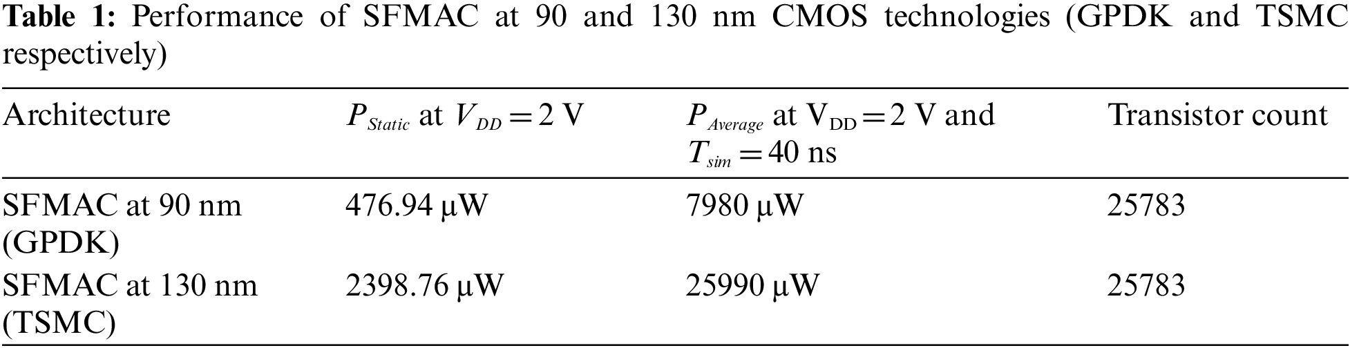
The SFMAC architecture is implemented in 90 and 130 nm CMOS technology (GPDK and TSMC, respectively). Tab. 1 compares the influence of the SFMAC architecture in various CMOS technologies for a particular input vector. Cadence Spectre Tool is used to measure the power usage of the implemented designs. The average power (PAverage) is calculated over a simulation time (Tsim) of 40 ns and at a clock frequency (fclk) of 83.33 MHz, while the static power is evaluated for a 2 V supply voltage (VDD). Since the transistor sizing is greater in 130 nm technology, the average power (PAverage) consumption in 130 nm (TSMC) is higher than 90 nm (GPDK) as it affects the load capacitance Cload. In the same way, device geometry affects static power consumption. As a result, a circuit with a larger device dimension can consume more static power. If αT is the activity factor, then CMOS dynamic power is calculated as Eq. (1):
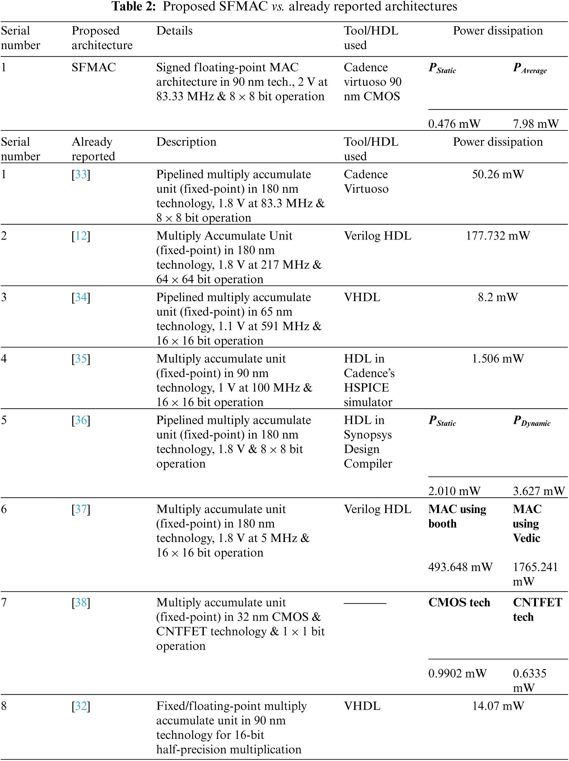
Tab. 2 shows a comparison of the proposed SFMAC architecture and existing MAC architectures in terms of power consumption. Since most of the available architectures in the literature use an HDL-based approach, comparing the proposed SFMAC architecture to those already present in the literature is difficult. On the other hand, the proposed architecture is implemented in a Cadence Virtuoso 90 or 130 nm technologies. Furthermore, almost all of the architectures described in the literature do not support signed operations & floating-point designs.

Figure 7: SFMAC architecture using ECC & ESC blocks
Although there are architectures that use clock signals just for data accumulation (in the register or accumulator), most of the architectures in the literature do not use any clocking signals. Asynchronous circuits do not have real-time applicability. As a result, the architecture's functional applicability must be further investigated. The architecture shown in [32] is designed for floating-point operation (signed), whereas most of the reported architectures, as discussed in Tab. 2, are dedicated to implementing fixed-point Multiply-Accumulate (unsigned) operation.
Although there are architectures that use clock signals just for data accumulation (in the register or accumulator), the majority of the architectures in the literature do not use any clocking signals. Asynchronous circuits don't have real-time applicability. As a result, the architecture's functional applicability must be further investigated. The architecture shown in [32] is designed for floating-point operation (signed), whereas most of the reported architectures, as discussed in Tab. 2 are dedicated for implementing fixed-point Multiply-Accumulate (unsigned) operation.
Tab. 2 reveals that the architectures in [12,33,34] consume considerably higher static and average power (in mW) than the proposed SFMAC architecture. The architectures in [35,36] are examined for 16-bit operations at 1 V and 8-bit operations at 1.8 V in 90 and 180 nm technologies. Even though the existing work described in [35,36] requires less power than the proposed SFMAC (the existing circuit's performance analysis is done with a supply voltage less than 2 V, while the SFMAC uses a supply voltage of 2 V), these two existing implementations can only execute MAC operations on unsigned fixed-point numbers. As a result, the MAC architectures in [35,36] have a restricted scope. Although the architecture defined in [37] is implemented in 180 nm technology with a 1.8 V supply voltage for 16-MAC operation, it consumes substantially more power than the SFMAC architecture. The implementation of the architecture listed in [38] is for 1-bit unsigned fixed-point MAC operation in 32 nm CMOS & CNTFET technology, so a comparison with an 8-bit SFMAC is meaningless. Despite the fact that the architecture described in [32] is the only existing MAC architecture capable of performing on signed floating-point operations, a comparative study with the proposed SFMAC reveals that SFMAC's efficiency in terms of power consumption is much better.
A novel approach for performing normalization is explained in this paper. The proposed normalization operation is categorized into Exponential Comparator Circuit (ECC) & Exponential Shifter Circuit (ESC). The ECC block performs a comparison between the exponents; at the same time, ESC is responsible for shifting the smaller number by the amount of difference between the exponents of the inputs. Further, a signed floating-point MAC architecture is also proposed using the novel normalization architecture. For design & implementation, the Cadence Spectre tool is used at CMOS 90 nm and TSMC 130 nm technologies. The results have proved that the proposed SFMAC architecture has used the least power than its recent counterpart & therefore, has applicability in low-power DSP architectures.
Funding Statement: This work was supported by Research Support Fund (RSF) of Symbiosis International (Deemed University), Pune, India
Conflicts of Interest: The authors declare that they have no conflicts of interest to report regarding the present study.
1. A. K. Dhindsa and R. Sarma, “Pipelined and clock gated MAC architecture design and implementation,” Far East Journal of Electronics and Communications, vol. 16, no. 1, pp. 607–621, 2016. [Google Scholar]
2. N. J. Babu and R. Sarma, “A novel low power multiply–accumulate (MAC) unit design for fixed point signed numbers,” Advances in Intelligent Systems and Computing, vol. 394, no. 1, pp. 675–690, 2016. [Google Scholar]
3. A. V. Ananthalakshmi and G. F. Sudha, “A novel power efficient 0.64-GFlops fused 32-bit reversible floating point arithmetic unit architecture for digital signal processing applications,” Microprocessors and Microsystems, vol. 51, no. 1, pp. 366–385, 2017. [Google Scholar]
4. M. Jayaprakash, A. Shanmugam and M. Mohamed, “Design and analysis of low power hybrid adder,” Journal of Theoretical and Applied Information Technology, vol. 58, no. 3, pp. 618–622, 2013. [Google Scholar]
5. R. Sarma, C. Bhargava and S. Jain, “A MUX based signed-floating-point MAC architecture using UCM algorithm,” Bulletin of the Polish Academy of Sciences: Technical Sciences, vol. 68, no. 4, pp. 835–844, 2020. [Google Scholar]
6. R. Sarma, C. Bhargava, S. Dhariwal and S. Jain, “UCM: A novel approach for delay optimization,” International Journal of Performability Engineering, vol. 15, no. 4, pp. 1190–1198, 2019. [Google Scholar]
7. S. Shanthala and S. Y. Kulkarni, “VLSI design and implementation of low power MAC unit with block enabling technique,” European Journal of Scientific Research, vol. 30, no. 4, pp. 620–630, 2009. [Google Scholar]
8. R. V. K. Pillai, D. Al-Khalili and A. J. Al-Khalili, “Low power architecture for floating point MAC fusion,” in Proc. IEEE Proc.-Computers and Digital Techniques, San Jose, CA, USA, pp. 288–296, 2000. [Google Scholar]
9. R. Warrier, C. H. Vun and W. Zhang, “A Low-power pipelined MAC architecture using baugh-wooley based multiplier,” in Proc. IEEE 3rd Global Conf. on Consumer Electronics (GCCE), Tokyo, Japan, pp. 505–506, 2014. [Google Scholar]
10. R. Sarma, C. Bhargava, S. Jain and V. K. Kamboj, “Application of ameliorated harris hawks optimizer for designing of low-power signed floating-point MAC architecture,” Neural Computing and Application, vol. 33, pp. 8893–8922, 2021. [Google Scholar]
11. P. A. Patil and C. Kulkarni, “A survey on multiply accumulate unit,” in Proc. Fourth Int. Conf. on Computing Communication Control and Automation (ICCUBEA), Pune, India, pp. 1–5, 2019. [Google Scholar]
12. P. Jagadees, S. Ravi and K. H. Mallikarjun, “Design of a high-performance 64-bit MAC unit,” in Proc. Int. Conf. on Circuits, Power and Computing Technologies, Nagercoil, India, IEEE, pp. 782–786, 2013. [Google Scholar]
13. R. Sarma, S. Dhariwal and S. Jain, “Design and analysis of a novel 8 × 8 bit signed/unsigned synchronous MAC architecture using clock gating scheme for fixed-point arithmetic,” in Proc. 2nd Int. Conf. on Intelligent Circuits and Systems, Punjab, India, pp. 423–429, 2018. [Google Scholar]
14. W. P. du Plessis, “Optimal MAC structures in an FPGA,” in Proc. IEEE AFRICON 6th Africon Conf. in Africa, IEEE, George, South Africa, pp. 333–336, 2002. [Google Scholar]
15. D. I. Jeon, K. B. Park and K. S. Chung, “HMC-MAC: Processing-in memory architecture for multiply-accumulate operations with hybrid memory cube,” IEEE Computer Architecture Letters, vol. 17, no. 1, pp. 5–8, 2017. [Google Scholar]
16. K. Chen, L. Chen, P. Reviriego and F. Lombardi, “Efficient implementations of reduced precision redundancy (RPR) multiply and accumulate (MAC),” IEEE Transactions on Computers, vol. 68, no. 5, pp. 784–790, 2018. [Google Scholar]
17. S. Ryu, N. Park and J. J. Kim, “Feedforward-cutset-free pipelined multiply–accumulate unit for the machine learning accelerator,” IEEE Transactions on Very Large-Scale Integration (VLSI) Systems, vol. 27, no. 1, pp. 138–146, 2018. [Google Scholar]
18. R. D. Rose, P. Romero and M. Lanuzzaa, “Double-precision dual mode logic carry-save multiplier,” Integration, vol. 64, no. 1, pp. 71–77, 2019. [Google Scholar]
19. V. M. Senthilkumar, S. Ravindrakumar, D. Nithya and N. V. Kousik, “A vedic mathematics-based processor core for discrete wavelet transform using FinFET and CNTFET technology for biomedical signal processing,” Microprocessors and Microsystems, vol. 71, no. 1, pp. 16–32, 2019. [Google Scholar]
20. H. Zhang, D. Chen and S. Ko, “New flexible multiple-precision multiply-accumulate unit for deep neural network training and inference,” IEEE Transactions on Computers, vol. 69, no. 1, pp. 26–38, 2019. [Google Scholar]
21. C. W. Tung and S. H. Huang, “A high-performance multiply-accumulate unit by integrating additions and accumulations into partial product reduction process,” IEEE Access, vol. 8, pp. 87367–87377, 2020. [Google Scholar]
22. A. Abdelgawad and M. Bayoumi, “High speed and area-efficient multiply accumulate (MAC) unit for digital signal processing applications,” in Proc. IEEE Int. Symp. on Circuits and Systems, New Orleans, LA, IEEE, pp. 3199–3202, 2007. [Google Scholar]
23. S. Deepak and B. J. Kailath, “Optimized MAC unit design,” in Proc. IEEE Int. Conf. on Electron Devices and Solid State Circuit (EDSSC), Bangkok, Thailand, IEEE, pp. 1–4, 2012. [Google Scholar]
24. T. Francis, T. Joseph and J. K. Antony, “Modified MAC unit for low power high speed DSP application using multiplier with bypassing technique and optimized adders,” in Proc. Fourth Int. Conf. on Computing, Communications and Networking Technologies (ICCCNT), Tiruchengode, India, pp. 1–4, 2013. [Google Scholar]
25. B. J. Xia, P. Liu and Q. D. Yao, “New method for high performance multiply-accumulator design,” Journal of Zhejiang University Science, vol. 10, no. 7, pp. 1067–1074, 2009. [Google Scholar]
26. U. Cini and O. Kurt, “A high performance multiply-accumulate unit with double carry-save scheme for 6-input LUT based reconfigurable systems,” in Proc. 9th Int. Conf. on Electrical and Electronics Engineering (ELECO), Bursa, Turkey, pp. 940–944, 2015. [Google Scholar]
27. T. Y. Kuo and J. S. Wang, “A low-voltage latch-adder based tree multiplier,” in Proc. IEEE Int. Symp. on Circuits and Systems, Seattle, WA, pp. 804–807, 2008. [Google Scholar]
28. M. J. Liao, C. F. Su, C. Y. Chang and A. C. H. Wu, “A Carry-select-adder optimization technique for high-performance booth-encoded wallace-tree multipliers,” in Proc. IEEE Int. Symp. on Circuits and Systems, ISCAS-2002, Phoenix-Scottsdale, AZ, USA, pp. 81–84, 2002. [Google Scholar]
29. T. V. Nguyen, N. T. Huynh, N. C. Vu, V. N. Kieu and S. C. Huang, “Optimizing compliant gripper mechanism design by employing an effective bi-algorithm: Fuzzy logic and ANFIS,” Microsystem Technologies, vol. 27, pp. 3389–3412, 2021. [Google Scholar]
30. N. L. Chau, T. P. Dao and V. T. T. Nguyen, “Optimal design of a dragonfly-inspired compliant joint for camera positioning system of nanoindentation tester based on a hybrid integration of jaya-ANFIS,” Mathematical Problems in Engineering, vol. 2018, pp. 1–16, 2018. [Google Scholar]
31. N. L. Chau, T. P. Dao and V. T. T. Nguyen, “An efficient hybrid approach of finite element method, artificial neural network-based multiobjective genetic algorithm for computational optimization of a linear compliant mechanism of nanoindentation tester,” Mathematical Problems in Engineering, vol. 2018, pp. 1–19, 2018. [Google Scholar]
32. H. Zhang, H. J. Lee and S. B. Ko, “Efficient fixed/floating-point merged mixed-precision multiply-accumulate unit for deep learning processors,” in Proc. IEEE Int. Symp. on Circuits and Systems (ISCAS), Florence, Italy, IEEE, pp. 1–5, 2018. [Google Scholar]
33. S. Shanthala, C. P. Raj and S. Y. Kulkarni, “Design and VLSI implementation of pipelined multiply accumulate unit,” in Proc. Second Int. Conf. on Emerging Trends in Engineering and Technology, Nagpur, India, IEEE, pp. 381–386, 2009. [Google Scholar]
34. T. T. Hoang, M. Själander and P. Larsson-Edefors, “A high-speed, energy-efficient two-cycle multiply-accumulate (MAC) architecture and its application to a double-throughput MAC unit,” IEEE Transactions on Circuits and Systems-I: Regular Papers, vol. 57, no. 12, pp. 3073–3081, 2010. [Google Scholar]
35. S. E. Esmaeili, A. J. Al-Kahlili and G. E. R. Cowan, “Low-swing differential conditional capturing flip-flop for LC resonant clock distribution networks,” IEEE Transactions on Very Large-Scale Integration (VLSI) Systems, vol. 20, no. 8, pp. 1547–1551, 2012. [Google Scholar]
36. N. Akbarzadeh, S. Timarchi and A. A. Hamidi, “Efficient multiply-add unit specified for DSPs utilizing low-power pipeline modulo 2n + 1 multiplier,” in Proc. 9th Iranian Conf. on Machine Vision and Image Processing, Tehran, Iran, Shahid Beheshti University, pp. 120–123, 2015. [Google Scholar]
37. A. Rahul Narasimhan and R. S. Subramanian, “High speed multiply-accumulator coprocessor realized for digital filters,” in Proc. IEEE Int. Conf. on Electrical, Computer and Communication Technologies (ICECCT), Coimbatore, India, pp. 1–4, 2015. [Google Scholar]
38. K. V. Karthikeyan, R. Babu, N. Mathan and B. Karthick, “Performance analysis of an efficient MAC unit using CNTFET technology,” in Proc. Recent Advances in Nano Science and Technology, Chennai, Tamilnadu, India, vol. 3, pp. 2525–2531, 2016. [Google Scholar]
 | This work is licensed under a Creative Commons Attribution 4.0 International License, which permits unrestricted use, distribution, and reproduction in any medium, provided the original work is properly cited. |