DOI:10.32604/cmc.2022.025798
| Computers, Materials & Continua DOI:10.32604/cmc.2022.025798 | |
| Article |
An Energy-Efficient 12b 2.56 MS/s SAR ADC Using Successive Scaling of Reference Voltages
1Department of Electronics Engineering, College of Electrical and Computer Engineering, Chungbuk National University, Cheongju, 28644, Korea
2Department of Electrical and Computer Engineering, COMSATS University Islamabad, Abbottabad Campus, Abbottabad, 22060, Pakistan
*Corresponding Author: HyungWon Kim. Email: hwkim@cbnu.ac.kr
Received: 05 December 2021; Accepted: 24 January 2022
Abstract: This paper presents an energy efficient architecture for successive approximation register (SAR) analog to digital converter (ADC). SAR ADCs with a capacitor array structure have been widely used because of its simple architecture and relatively high speed. However, conventional SAR ADCs consume relatively high energy due to the large number of capacitors used in the capacitor array and their sizes scaled up along with the number of bits. The proposed architecture reduces the energy consumption as well as the capacitor size by employing a new array architecture that scales down the reference voltages instead of scaling up the capacitor sizes. The proposed 12-bit SAR ADC is implemented in Complementary Metal Oxide Semiconductor (CMOS)
Keywords: Low voltage low power; successive approximation register; analog to digital converter; switching energy
Wireless sensor networks and implantable biomedical devices has been gaining popularity in the recent years. These applications require low power consumption because of their limited power budget while achieving optimum performance. Also, it is required to include an analog to digital converter (ADC) for converting sensor data to digital. So, energy and area efficient ADCs plays a pivotal role.
For many ADC architectures, analog circuits are often employed such as operational amplifiers, which usually consume high energy. But the successive approximation register (SAR) ADCs, however, only need a simple analog circuit like a comparator since they carry out the rest of the operations using the digital circuits. SAR ADCs can, therefore, result in an improved performance and reduced power consumption. Despite these advantages, however, SAR ADCs are not selected for high resolution applications, because their capacitor array requires an excessively large capacitors for high resolution. Various techniques have been proposed to overcome this short coming of SAR ADC. The technique in [1] reduced the supply voltage to reduce the energy consumption, while [2] proposed the merged capacitor switching scheme, to reduce the switching power. In [3,4], a reduction in total capacitor size is realized by using the split capacitor scheme and the R&C Hybrid scheme.
Literature reveals several techniques to reduce the capacitor array size without digital calibration for fully differential architecture [5]. To reduce the capacitor array size by half a top plate sampling technique is used in [6], but at the expense of non-linearity and common mode input dependency. In [7] a digital to analog converter (DAC) configurable window switching technique to ensure reusing the capacitors in DAC is incorporated in SAR ADCs for overall smaller capacitances. However, the benefit of energy efficiency drops. In order to reduce the switching energy and improve the DAC linearity floating DAC switching technique is presented in [8].
In this paper, we propose a SAR ADC architecture based on successive scaling of the reference voltages instead of conventional scaling of capacitor size to reduce the switching energy consumption and chip area.
The rest of this paper is organized as follows: Section 2 describes the general architecture of SAR ADCs. Section 3 presents the proposed architecture and the analysis of its switching energy. Section 4 describes a 12-bit ADC implementation based on the proposed architecture. Section 5 analyzes the performance of the 12-bit ADC implementation followed by the conclusions in Section 6.
Fig. 1 shows a structure of a general SAR ADC, which consists of a DAC capacitor array, a comparator circuit, and a SAR control logic. The DAC capacitor array combines the functionality of digital to analog conversion and sample and hold to produce an approximated common mode voltage
Initially,
Then, the comparator output is given by Eq. (2).
The comparator output determines the MSB bit of the digital output. If the output voltage
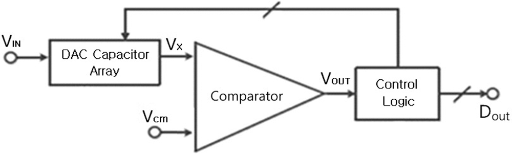
Figure 1: Block diagram of a general SAR ADC
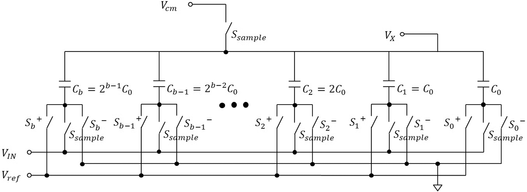
Figure 2: Conventional capacitor array of a b-bit SAR ADC
The above process is repeated for successive capacitors in the array. In each stage, the updated value of
Here,
During every bit cycle, the connections of the capacitors are changed. This section analyzes the switching energy [10] of the conventional architecture and the proposed scheme. For simplicity of analysis, a 2-bit capacitor array is selected in this section. A conventional 2-bit capacitor array is first analyzed, which is illustrated in Fig. 3.
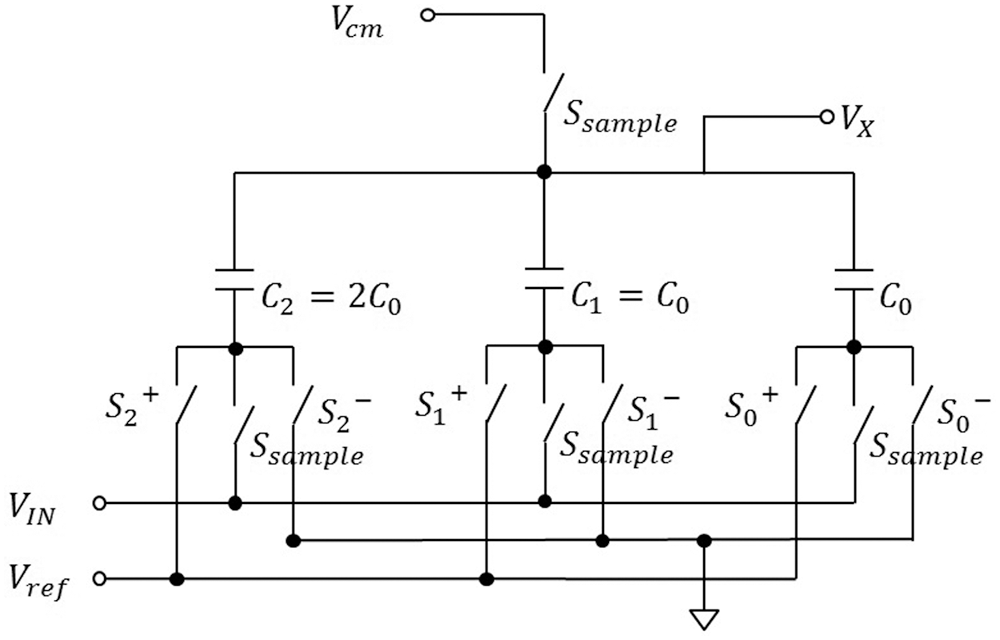
Figure 3: Capacitor array of a conventional 2-bit SAR ADC
At time
Since
Here
In the 2nd iteration of the approximation process,
Fig. 4 shows the proposed capacitor array architecture. The proposed architecture applies to each capacitor different reference voltage
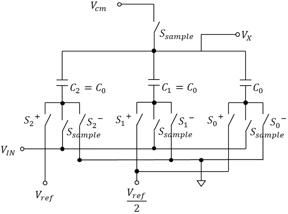
Figure 4: Capacitor array of a 2-bit SAR ADC based on scaled reference
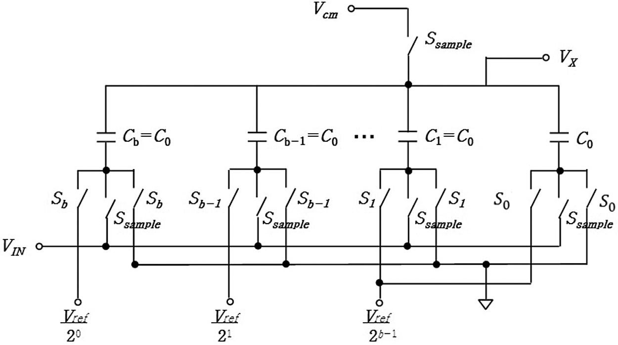
Figure 5: Capacitor array of a b-bit SAR ADC based on scaled reference
It is evident from Eqs. (9) and (11) that the proposed SAR ADC architecture can substantially reduce the energy consumption as well as the size of capacitor array compared to the conventional architecture. For another example, Fig. 5 illustrates a b-bit SAR ADC based on the proposed scaled reference. Eqs. (12) and (13) compares the energy consumption of the capacitor array for the case of a conventional b-bit SAR ADC with the proposed one in Fig. 5.
By comparing Eqs. (12) and (13), it is observed that the energy reduction effect of the proposed SAR ADC is becoming drastically increasing. While the proposed architecture can substantially reduce the energy consumption and capacitor size, however, it has a restriction on the input dynamic range due to the reduced DAC maximum output voltage. This restriction can be acceptable for many ultra-low power and Internet of Things (IoT) application.
Conventional:
Proposed:
To evaluate the performance of the proposed architecture, a 12-bit SAR ADC is implemented based on the proposed successive reference scaling architecture, which is shown in Fig. 6. We implemented it in a fully differential structure to suppress the common mode noise. It also helps to inhibit even harmonic noise, thus improving the dynamic performance of ADC. The key building blocks of the implementation consists of bootstrapped switches, a dynamic comparator, a SAR control logic, and capacitor array DACs including the scaled reference voltages. The following sections describe the design considerations of the building blocks.
An input sampling switch often has large impact on the performance of ADC circuits. To improve the linearity of the switch’s transfer function, bootstrapped switch circuits have been widely studied. In this paper, thick gate oxide
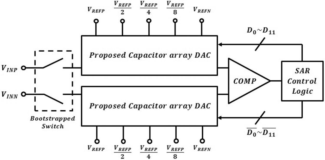
Figure 6: Block diagram of a proposed 12-bit SAR ADC
Fig. 7 explains the simplified operation of the cascaded bootstrapped switch circuit. Input clock is only a single-phase clock
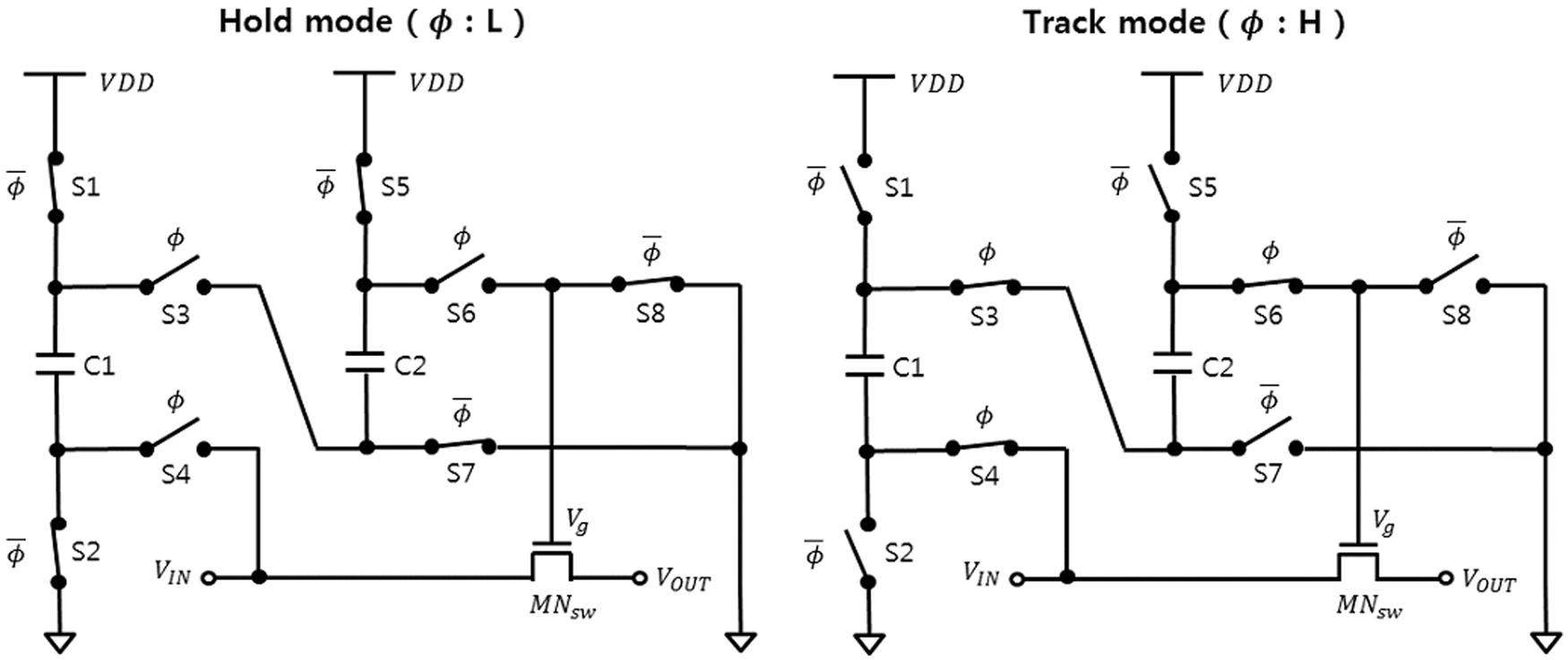
Figure 7: The operation of the bootstrapped switch
When
4.2 Hybrid Structure of Capacitor Array
While the proposed architecture can substantially reduce the switching energy of the capacitor array, it has some limitations. The input dynamic range is reduced by the reduced reference voltage. Generating different reference voltages can be challenging if it requires a large number of reference voltages. To alleviate this challenge, we propose a hybrid structure of capacitor array, which combines the proposed reference-scaling array along with the conventional capacitor-scaling array. For example, Fig. 8 shows a 12-bit capacitor array using the hybrid architecture. It employs the reference-scaling architecture for a 4-bit segment (Bit8~Bit5) and uses the capacitor-scaling architecture for the rest of the array (Bit11~Bit9 and Bit4~Bit0). We assume that these 4 reference voltages can be provided by a power management integrated circuit (PMIC) or internal voltage regulators.
Furthermore, the size of the capacitor array can be further reduced by using a split capacitor. The split capacitor is used to split the array into a least significant bit (LSB) array and a MSB array. Fig. 8 shows a split capacitor of size
In the example of Fig. 8, the proposed hybrid array architecture reduces the overall capacitor size by
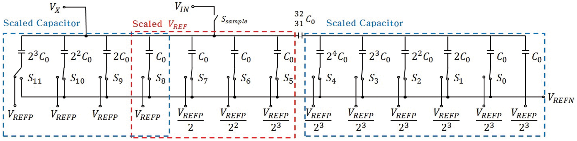
Figure 8: Architecture of proposed 12-bit capacitor array DAC
In addition, the proposed architecture eliminates the needs for an extra reference voltage
In SAR ADCs, the comparator also considerably contributes to the power consumption. We employ a two-stage dynamic circuit design similar to [13]. The comparator is shown in Fig. 10. The first stage is a voltage amplification stage. The second stage is a latch structure with cross-coupled inverters acting as a positive-feedback amplifier. It obtains the rail-to-rail digital output (
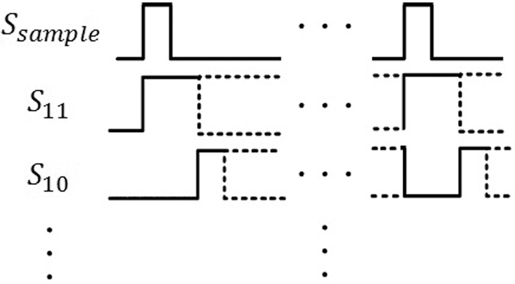
Figure 9: Timing diagram of capacitor array
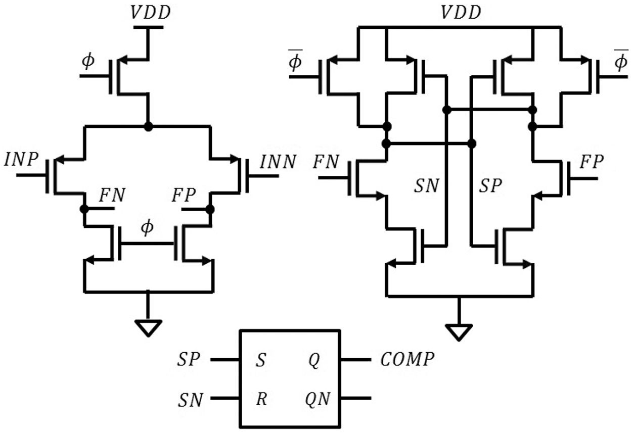
Figure 10: Architecture of dynamic comparator
For SAR control logic, asynchronous control circuits have been often used to achieve high speed [14]. The circulation behavior of the asynchronous circuits, however, can incur serious stability problems, when the asynchronous circuits experience variations in the process, voltage, and temperature. To avoid such risk, therefore, we employ synchronous control circuit based on a ring counter structure. Fig. 11 shows the SAR control circuit used by the proposed SAR ADC.
The operation of the control circuit is summarized below. For each conversion, in the first cycle, the End of Conversion
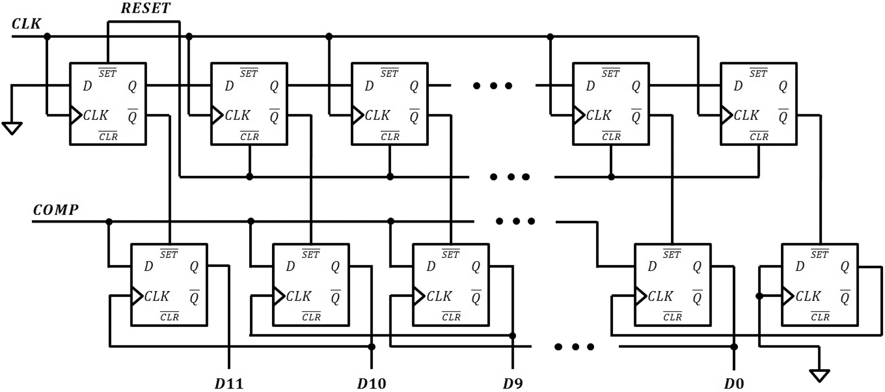
Figure 11: Architecture of SAR control logic
In each clock cycle, one of the outputs in the ring counter sets a DFF in the code register. The output of this DFF which is set by the ring counter is used as the clock signal for the previous DFF. At the rising edge of the clock, this DFF loads the result from the comparator. At the end of the conversion,
The proposed SAR ADC was implemented and fabricated using a 0
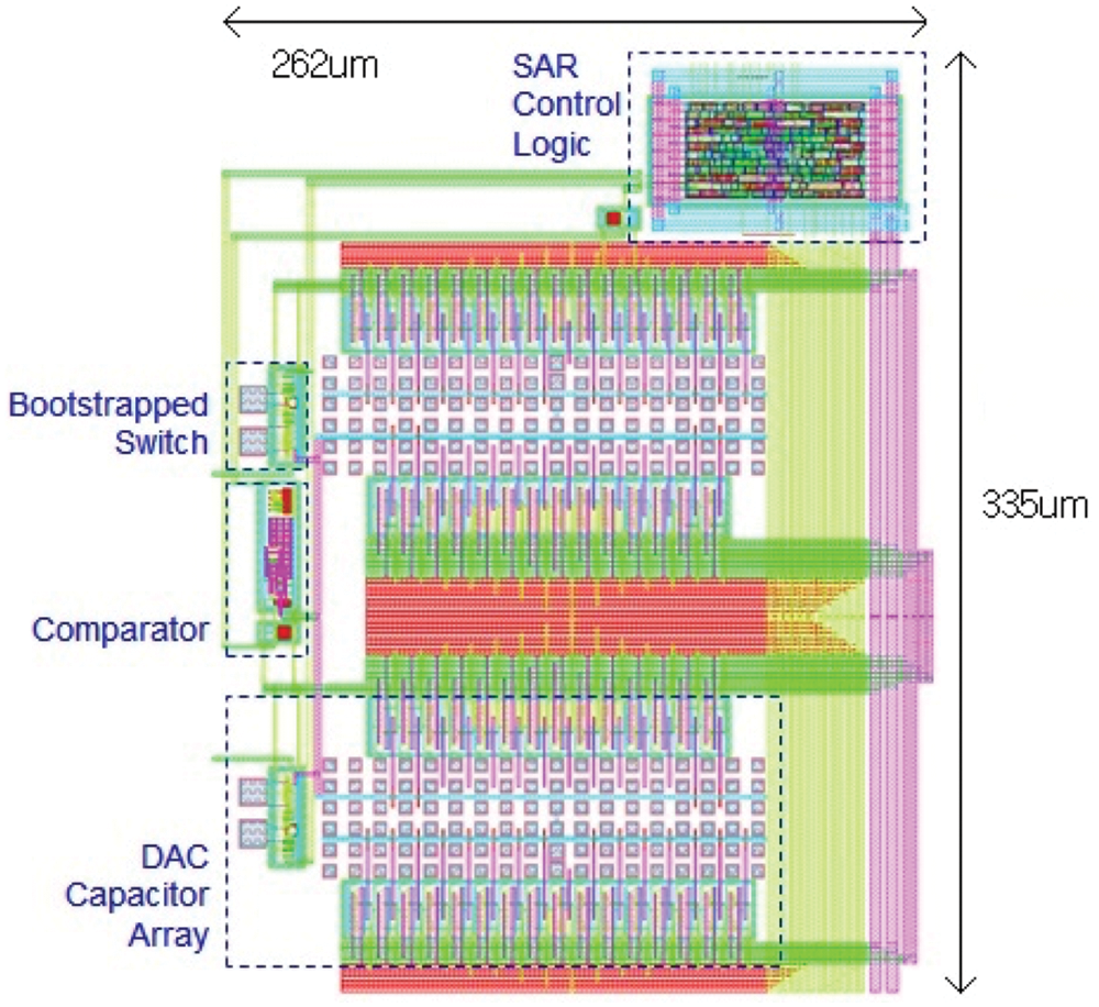
Figure 12: Layout view of proposed 12-bit SAR ADC
Fig. 13 compares the energy consumption of the proposed SAR ADC with various previous SAR ADCs: conventional, split capacitor, and R&C Hybrid SAR ADC. For fair comparison of various capacitor array architectures, the same dynamic comparator and SAR control circuit are used in all ADCs architectures compared above. The proposed SAR ADC provides the lowest energy consumption throughout all range of input voltages (X-axis indicates the corresponding digital output code).
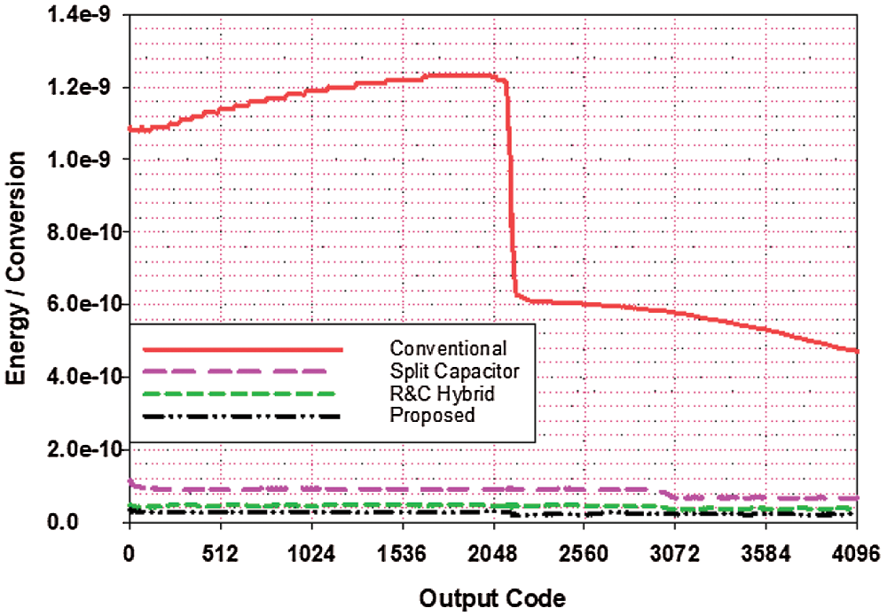
Figure 13: Comparison results of the energy consumption
Fig. 14 shows spectral analysis for the output of the proposed SAR ADC. Under a supply voltage of
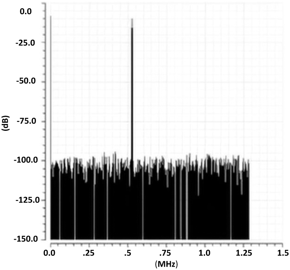
Figure 14: Output spectrum operating at 2.56 MS/s
Under the same operating conditions, we conducted detailed comparison between the proposed SAR ADC and the previous SAR ADCs. Tab. 1 demonstrates that the proposed SAR ADC achieves the lowest power consumption. It reduces the power consumption by
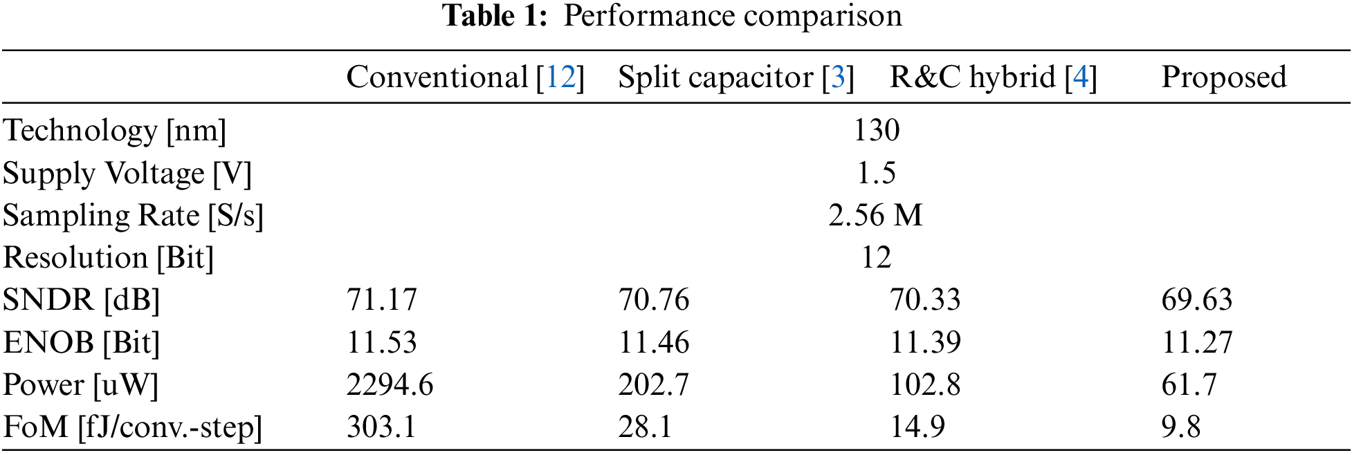
This paper proposed an energy-efficient architecture of successive approximation register (SAR) analog to digital converter (ADC) based on successive scaling of reference voltage. The proposed architecture incorporates a hybrid array architecture that scales down the reference voltages instead of scaling up the capacitor sizes. To illustrate the concept, a 12-bit SAR ADC is implemented in Complementary Metal Oxide Semiconductor (CMOS) 0.13um library using Cadence Virtuoso design suite and compared with conventional SAR ADC, SAR ADC with split capacitor, and Resistor & capacitor (R&C) Hybrid SAR ADC. Simulation results demonstrates an overall energy saving of
Funding Statement: This work was partly supported by Institute of Information & communications Technology Planning & Evaluation (IITP) grant funded by the Korea government(MSIT) (No.2020-0-01304, Development of Self-learnable Mobile Recursive Neural Network Processor Technology) and also supported by the MSIT(Ministry of Science and ICT), Korea, under the Grand Information Technology Research Center support program(IITP-2020-0-01462) supervised by the IITP(Institute for Information & communications Technology Planning & Evaluation)''. And also financially supported by the Ministry of Small and Medium-sized Enterprises(SMEs) and Startups(MSS), Korea, under the ``Regional Specialized Industry Development Plus Program(R&D, S3091644)'' supervised by the Korea Institute for Advancement of Technology(KIAT) and supported by the AURI(Korea Association of University, Research institute and Industry) grant funded by the Korea Government(MSS: Ministry of SMEs and Startups). (No. S2929950, HRD program for 2020).
Conflicts of Interest: The authors declare that they have no conflicts of interest to report regarding the present study.
1. Z. Zhu and Y. Liang, “A 0.6-V 38-nW 9.4-ENOB 20-kS/s SAR ADC in 0.18-um CMOS for medical implant devices,” IEEE Transactions on Circuits and Systems, vol. 62, no. 9, pp. 2167–2176, 2015. [Google Scholar]
2. V. Hariprasath, J. Guerber, S. H. Lee and U. K. Moon, “Merged capacitor switching based SAR ADC with highest switching energy-efficiency,” Electronics Letters, vol. 46, no. 9, pp. 620–621, 2010. [Google Scholar]
3. C. C. Liu, S. J. Chang, G. Y. Huang, Y. Z. Lin and C. M. Huang, “A 1V 11fJ/Conversion-Step 10b 10 MS/s Asynchronous SAR ADC in 0.18 μm CMOS,” in Proc. IEEE Symp. on VLSI Circuits, Honolulu, Hawaii, USA, pp. 241–242, 2010. [Google Scholar]
4. J. H. Byun, J. S. Park, W. K. Kim, Y. S. Cho, Y. S. Lee et al., “A 12b 60 MS/s 0.11 μm Flash-SAR ADC using mismatch-free shared sampling network,” in Proc. ISOCC, Gyeongju, South Korea, pp. 79–80, 2015. [Google Scholar]
5. M. Zhang, K. Noh, X. Fan and E. Sánchez-Sinencio, “A 0.8-1.2 V 10-50 MS/s 13-bit Subranging Pipelined-SAR ADC using a temperature-insensitive time-based amplifier,” IEEE Journal of Solid-State Circuits, vol. 52, no. 11, pp. 2991–3005, 2017. [Google Scholar]
6. C. Liu, S. Chang, G. Huang and Y. Lin, “A 10-bit 50-MS/s SAR ADC with a monotonic capacitor switching procedure,” IEEE Journal of Solid-State Circuits, vol. 45, no. 4, pp. 731–740, 2010. [Google Scholar]
7. Y. Chung, Q. Zeng and Y. Lin, “A 12-bit SAR ADC with a DAC-configurable window switching scheme,” IEEE Transactions on Circuits and Systems I: Regular Papers, vol. 67, no. 2, pp. 358–368, 2020. [Google Scholar]
8. E. Martens, B. Hershberg and J. Craninckx, “A 69-dB SNDR 300-MS/s two-time interleaved pipelined SAR ADC in 16-nm CMOS FinFET with capacitive reference stabilization,” IEEE Journal of Solid-State Circuits, vol. 53, no. 4, pp. 1161–1171, 2018. [Google Scholar]
9. R. J. Baker, “CMOS Circuit Design, Layout, and Simulation. Manhattan, New York, USA: Wiley Online Library, IEEE Press, 2010. [Online]. Available: https://onlinelibrary.wiley.com/doi/book/10.1002/9780470891179. [Google Scholar]
10. B. P. Ginsburg and A. P. Chandrakasan, “An energy- efficient charge recycling approach for a SAR converter with capacitive DAC,” in Proc. IEEE Int. Symp. on Circuits and Systems, Kobe, Japan, pp. 184–187, 2005. [Google Scholar]
11. A. Shikata, R. Sekimoto and H. Ishikuro, “A 0.5 V 65 nm-CMOS single phase clocked bootstrapped switch with rise time accelerator,” in Proc. APCCAS, Kuala, Malaysia, pp. 1015–1018, 2010. [Google Scholar]
12. D. Zhang, A. Bhide and A. Alvandpour, “A 53-nW 9.1-ENOB 1-kS/s SAR ADC in 0.13-m CMOS for medical implant devices,” IEEE Journal of Solid-State Circuits, vol. 47, no. 7, pp. 1585–1593, 2012. [Google Scholar]
13. M. V. Elzakker, E. V. Tuijl and P. Geraedts, “A 10-bit charge-redistribution ADC consuming 1.9 W at 1 MS/s,” IEEE Journal of Solid-State Circuits, vol. 45, no. 5, pp. 1007–1015, 2010. [Google Scholar]
14. S. W. M. Chen and R. W. Brodersen, “A 6-bit 600-MS/s 5.3 mW asynchronous ADC in 0.13- CMOS,” IEEE Journal of Solid-State Circuits, vol. 41, no. 12, pp. 2669–2680, 2006. [Google Scholar]
 | This work is licensed under a Creative Commons Attribution 4.0 International License, which permits unrestricted use, distribution, and reproduction in any medium, provided the original work is properly cited. |