DOI:10.32604/cmc.2022.023452
| Computers, Materials & Continua DOI:10.32604/cmc.2022.023452 | |
| Article |
Process Tolerant and Power Efficient SRAM Cell for Internet of Things Applications
1Faculty of Engineering and Technology, Multimedia University, Melaka, 75450, Malaysia
2School of Engineering and Computing, Manipal International University, Nilai, 71800, Malaysia
3Electronics and Communication Engineering Department, NIIT University, Neemarana, 301705, India
*Corresponding Author: T. G. Sargunam. Email: sargunam.thirugnanam@miu.edu.my
Received: 09 September 2021; Accepted: 09 February 2022
Abstract: The use of Internet of Things (IoT) applications become dominant in many systems. Its on-chip data processing and computations are also increasing consistently. The battery enabled and low leakage memory system at subthreshold regime is a critical requirement for these IoT applications. The cache memory designed on Static Random-Access Memory (SRAM) cell with features such as low power, high speed, and process tolerance are highly important for the IoT memory system. Therefore, a process tolerant SRAM cell with low power, improved delay and better stability is presented in this research paper. The proposed cell comprises 11 transistors designed with symmetric approach for write operations and single ended circuit for read operations that exhibits an average dynamic power saving of 43.55% and 47.75% for write and 35.59% and 36.56% for read operations compared to 6 T and 8 T SRAM cells. The cell shows an improved write delay of 26.46% and 37.16% over 6 T and 8 T and read delay is lowered by 50.64% and 72.90% against 6 T and 10 T cells. The symmetric design used in core latch to improve the write noise margin (WNM) by 17.78% and 6.67% whereas the single ended separate read circuit improves the Read Static Noise Margin (RSNM) by 1.88x and 0.33x compared to 6 T and 8 T cells. The read power delay product and write power delay product are lower by 1.94x, 1.39x and 0.17x, 2.02x than 6 T and 8 T cells respectively. The lower variability from 5000 samples validates the robustness of the proposed cell. The simulations are carried out in Cadence virtuoso simulator tool with Generic Process Design Kit (GPDK) 45 nm technology file in this work.
Keywords: SRAM cell; low power; process efficient; read stability; write ability; static noise margin; PVT variation; internet of things
The Internet of Things (IoT) applications are becoming part and parcel of our daily life. IoT applications are used in almost all the industry verticals ranging from manufacturing, healthcare, tourism, agriculture, transportation, tele-communication to many others. The IoT revolution does not leave any industry behind. There is a tremendous growth and a huge demand for the IoT based systems. Some of the example applications are smart cities, smart buildings, smart homes, smart agriculture and smart systems. The technologists confirm that IoT and its applications will be driving the human sensations in the future [1]. The IoT application connects a multiple number of portable and battery-operated gadgets by using a wireless sensor network (WSN). The most critical requirements for these IoT application devices are smaller chip area and lesser power consumption [2]. The WSN performs a vital role in these applications. Basically, it offers the communication and connectivity to gather data between the nodes and the base-station for further processing. The nodes communicate with the base-station using wireless protocols [3]. The memory has become the major portion of these modern architectures. The design of static random-access memory (SRAM) is becoming highly critical for any trending application and is one of the most common memory architectures due to its performance [4].
The IoT based low power applications demand the cache memory designed with SRAM due to its high performance and low power features. There are many proposed design techniques for low power and energy efficient SRAM cell with its merits and demerits [5,6]. It is well discussed in the literature that memory cell normally consumes larger power from the overall power of the system. In low power IoT based system-on-chip (SoC) applications, 40–50% average dynamic power is constantly consumed by SRAM memory [7,8]. The conventional cells such as 6 T and 8 T are proven that they are not suitable for any low power applications. The main generic challenges of these SRAM memory are high power consumption, degraded stability, leakage current, short channel effects (SCEs). Over the years, many researchers have suggested and developed many different approaches and techniques to lower the overall power of cache memory [9,10] e.g., differential operation, loop cutting, staff effect, decoupled read circuit, power gating, single bit line operation, lower the supply voltage and schmitt trigger approach [11–15]. The SRAM cells with separate write and read circuits improve significant stability [16,17]. Although there are many different techniques used to design SRAM cells, the conventional cells are not so suitable for the current and trending IoT applications [18,19] due to its low power requirements. Although, the common challenges may be overcome by these SRAM design techniques, the variation of process, voltage, and temperature (PVT) is normally added up to these challenges. A power efficient SRAM cell is critically required to address the above challenges and to exhibit immunity to process variation with operational reliability. Hence, a process tolerant and power efficient SRAM cell is proposed and designed with the following salient features and novelties in this work:
• The latch circuit is totally disconnected so then the data switches quickly on the nodes during the write operations which results the dynamic power consumption less due to lesser discharging at the bit-lines (BL and NBL).
• There are two signals used which play an important role instead of word-line (WL) for the write operations to enhance the write ability.
• The single ended and separate read circuit reduces the read power, improves the read stability and overall read performance.
• The three N-channel metal oxide semiconductor (NMOS) transistors connected in series of the read circuit reduces the static power and leakage current due to the stack effect.
The rest of the paper is organized as follows: The Section 2 highlights the related works in terms of the comparative SRAM cells. Section 3 presents the detailed design of proposed cell structure as well as the working principles. Further, Section 4 incorporates the various analyses, observations, and results outcome of the proposed 11 T cell and comparative cells 6 T [20], 8 T [21], 10 T [22], and 11 T [23] with respect to power consumption, delay, energy efficiency, stability, area, and PVT variations. Section 5 discuss the Monte-Carlo simulation results and statistical variability. Finally, the Section 6 concludes the paper.
The conventional cells such as 6 T cell and 8 T cell are industry standard architectures which normally used as the reference to benchmark the SRAM performance. The researchers have proposed many budding SRAM cell topologies with enhanced outcome while comparing with these traditional topologies [11–15]. However, in common these cells suffer from conflict between read and operations, degraded stability, half select issue, write failures etc. Further, if the read static noise margin is improved, then it may affect the write operation. The researchers have also forecasted that the process variation may limit the required minimum voltage for the write and read operations. There have been so many improved SRAM cells proposed by researchers [11–15] to enhance the outcomes against conventional 6 T cell.
In this research, the conventional 6 T [20], standard 8 T [21], low power and high speed 10 T [22] and multi-bit error tolerant 11 T [23] have been chosen for review and for benchmarking. These cells are redesigned at schematic and layout in same environment and then compared against the proposed cell. All these cells’ schematic representation is shown in Figs. 1 and 2. The operational specifications of the selected cells are highlighted in Tab. 1. The comprehensive process variation analysis of the proposed cell and the selected cells are discussed in detail in this paper. Despite having so many different cells with various techniques, the research is still open for SRAM cell design in terms of minimizing power, improving performance, better write ability and read stability, less leakage current, energy efficient and process tolerance for IoT applications.
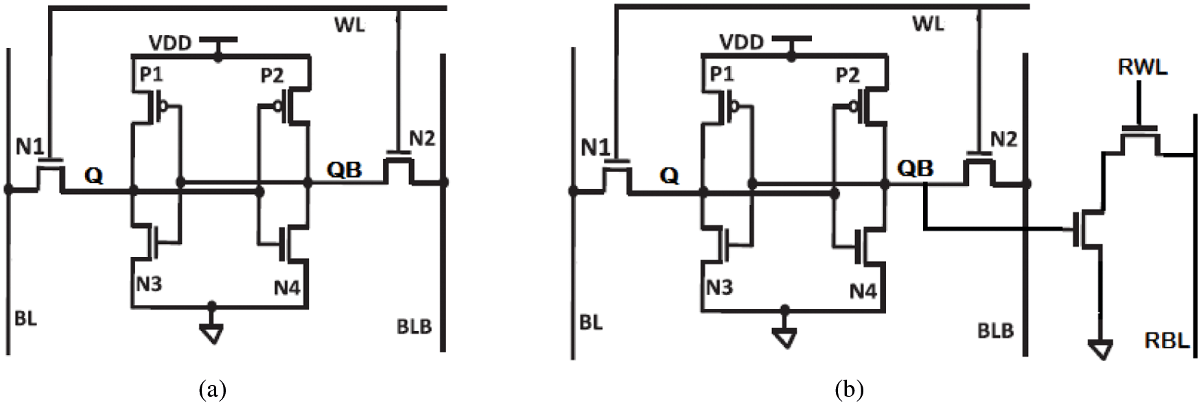
Figure 1: SRAM structure: (a) 6 T SRAM cell [20] (b) 8 T SRAM cell [21]
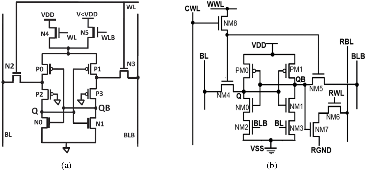
Figure 2: SRAM structure: (a) 10 T SRAM cell [22] (b) 11 T SRAM cell [23]
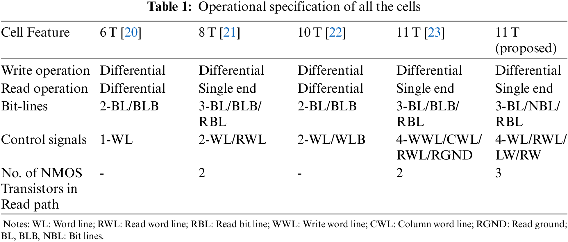
All the selected SRAM cells perform the write and read operations on differential mode except 8 T [21] and 11 T [23] cell work on single end read operation. The number of bit-lines are 2 to 3 in all the cells. The common control signals are WL for write and RWL for read operations. The number of transistors used for single end read operation is 2 and 3 for 8 T [21] and 11 T [23] cells. Summarizing all the highlighted challenges, a power efficient and process tolerant 11 T SRAM cell is proposed in this paper. Besides the comprehensive analysis of proposed 11 T cell, several comparative analyses are also carried out and compared with selected conventional 6 T [20], standard 8 T [21] and low power and high speed 10 T [22] and multi-bit error tolerant 11 T [23] cells.
3 Proposed Process Tolerant and Power Efficient SRAM Cell
The schematic architecture of the proposed cell is shown in Fig. 3. The proposed cell consists of 11 transistors (11 T) with separate write and read circuits to minimize the power and enhance the read static noise margin without any compromise on delay. The proposed cell has two inverters on both sides. The left side inverter is composed by transistors PM1, P-channel metal oxide semiconductor (PMOS) and NM1, N-channel metal oxide semiconductor (NMOS) and right one by PM2 and NM2. The NM3 and NM4 tail transistors play a vital role during the write operations. They pull either logic high or low at output nodes which improves the cell's write ability. The signals LW and RW control the switching activity of these two tail transistors. The inverter performs write operation quicker without waiting for the bit-line to discharge and hence it saves reasonable dynamic power. The BL and NBL bit-lines are connected to Q and NQ output nodes through the NMOS transistors NA1 and NA2. These two transistors (NA1 and NA2) function as access transistors. The write mode operation is jointly performed by the word-line WL and the LW and RW signals in this proposed cell. For the write operation, upon asserting the word-line WL to high, the access transistors NA1 and NA2 are turned ON and the LW and RW signals are alternatively switched ON so that the corresponding data in bit lines can be transferred faster to Q and NQ nodes respectively.
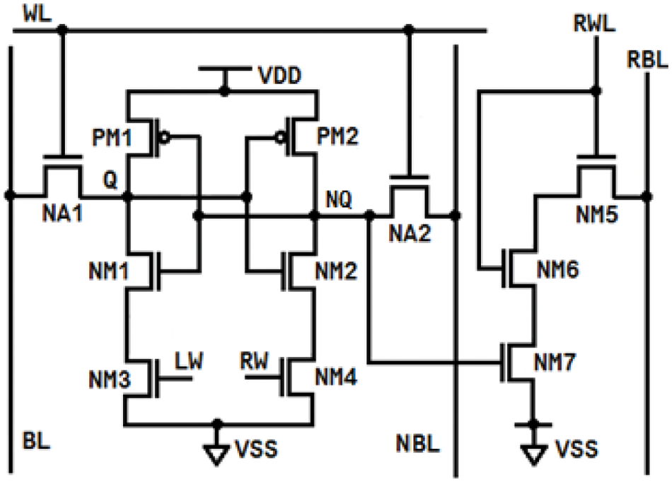
Figure 3: Schematic diagram of proposed 11 T Cell
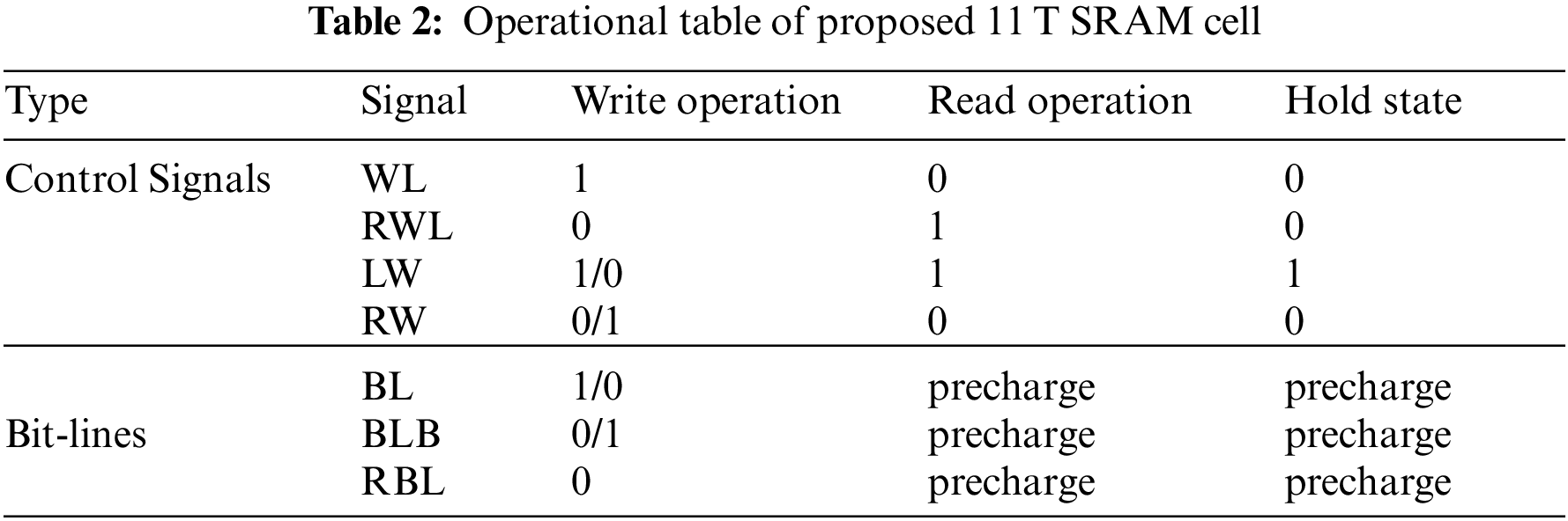
The single end read circuit is designed with three NMOS transistors NM5, NM6 and NM7 to improve the cell's read stability. The NM5 and NM6 transistors behave as read pass-transistors which controls the read word-line (RWL). The output NQ is connected to the gate of NM7 transistor. During the read mode and hold mode operations, the LW and RW signals are assigned to be high and low as the read operation is done independently. The output nodes are separated from the bit-lines during read and hold mode operations through which the proposed cell's static noise margin (SNM) has been significantly improved. The use of three transistors is to have stack effect which helps to reduce the leakage current in hold mode. The current flow is also limited from read bit-line to ground and hence the power dissipation is less. The status of control signals for write, read and hold state is presented in Tab. 2.
3.2 Working Principle of the Proposed Cell
The proposed 11 T cell is designed and implemented in 45 nm complementary metal oxide semiconductor (CMOS) technology. A uniform device size has been applied to PMOS and NMOS transistors for reasonable comparison. The 150 nm/45 nm size has been used for all the PMOS transistors and 120 nm/45 nm is applied for all the NMOS transistors. This combination of device sizing provides the nominal voltage transfer characteristics (VTC). The 1 V supply voltage at 27°C temperature is applied for all the operations.
The transistors NA1 and NA2 flip the data quickly at the storage nodes due to the proposed cell's dynamic nature. During the write operation, the word-line WL is asserted to high and read word-line RWL and PC (to precharge RBL) are set to low after the data is assigned on bit-lines BL and NBL. The LW and RW signals play a significant role instead of WL for the write operations to enhance the write ability. The write circuit of the proposed 11 T cell is shown in Fig. 4. The proposed cell signaling scheme and the status of bit lines and control signals of write operation is plotted in Fig. 6.
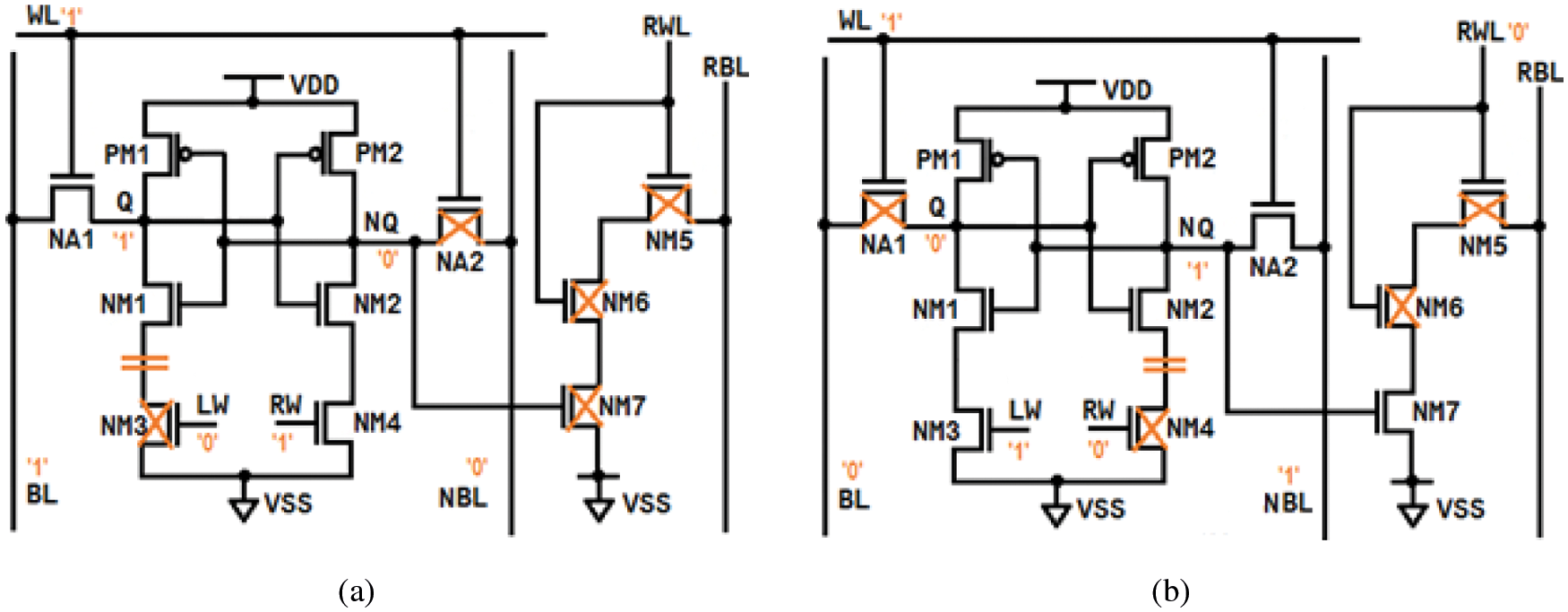
Figure 4: Write mode: (a) Write ‘1’ operation (b) Write ‘0’ operation
For write ‘1’ operation, the bit-line BL is set to high, NBL is set to low and WL is asserted to high. Prior to asserting WL, the LW is set to low and RW signal is high so that NM3 or NM4 transistor is either disconnected or connected from the ground. Once the NA1 and NA2 transistors are turned ON, the respective data in bit-line BL is transferred to Q. When bit-line NBL is assigned to ‘0’, the transistor NM3 turns off due to LW is kept at low. This will disconnect pull down path of left inverter. Hence, the output Q is quickly flipped to high before NBL discharges completely without any waiting.
For write ‘0’ operation, the bit-line NBL is set to high and BL to low. Prior to asserting the WL, the LW is assigned to high and RW signal to low so that NM3 or NM4 transistor is either connected or disconnected from the ground and which causes the data to be stored in NQ. When BL is assigned to ‘0’, the transistor NM4 turns off due to RW is also set to ‘0’ and disconnects pull down path of right inverter which flip the node NQ to high quickly without any waiting for bit-line (BL) to completely discharge. The effect of disconnecting the pull-down path causes low power consumption and improved write access time.
For read operation, the WL is not used and hence set to low. Both bit-lines BL, NBL must be precharged during read operation and RWL is connected to VDD. The separate read circuit would perform either read ‘0’ or read ‘1’ operation which depends on the output data in node NQ. When NQ holds data ‘0’, the transistors in the read path (NM5 and NM6) are turned ON whereas NM7 is turned OFF which will disconnect RBL from ground. The read path is open now and does not allow RBL to discharge. Therefore, RBL holds the pre-charged voltage level which is treated as read 1 operation. If NQ holds data ‘1’, all three transistors (NM5, NM6 and NM7) in read path will turn ON which allows the RBL to discharge fully and sense amplifier will interpret this voltage fall on RBL as read 0. The read circuit is shown in Fig. 5. The proposed cell signaling scheme and the status of bit lines and control signals during read operation is plotted in Fig. 6.
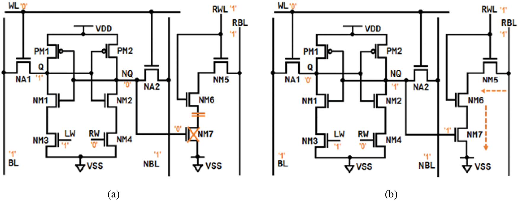
Figure 5: Read mode: (a) Read ‘1’ Operation (b) Read ‘0’ Operation
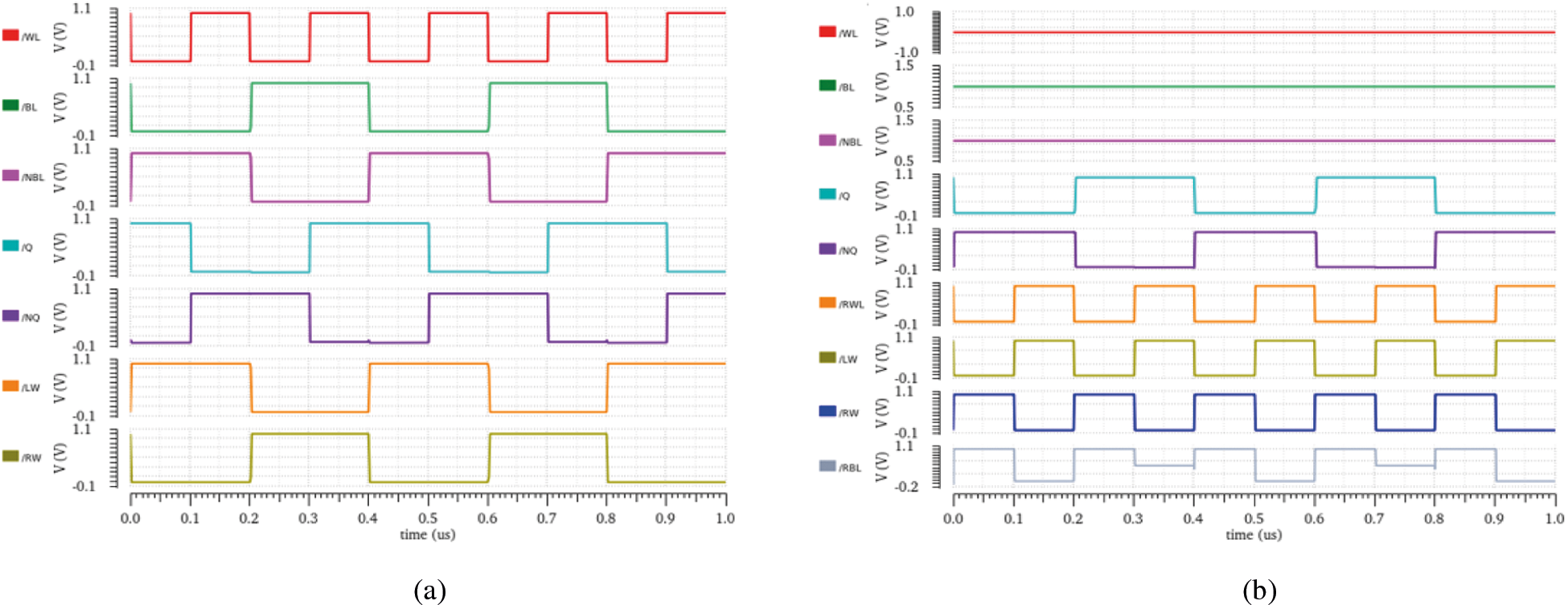
Figure 6: Waveform of the proposed 11 T cell (a) Write operation (b) Read operation
In the hold mode, the access transistors NA1 and NA2 are disconnected from the bit-lines BL and NBL by setting WL to low. The RWL is also set to ground and bit-lines BL and NBL are precharged to VDD. Therefore, the cell is in standby or hold mode. The cell will continue to hold the previous voltage level.
4 Simulation Results and Discussion
The Cadence virtuoso simulator tool using Generic Process Design Kit (GPDK) for 45 nm technology is used to carry out all the simulations in this research work. The respective cells are designed and simulated at 1-V supply voltage and at 27°C temperature. An equal device size is applied for all PMOS and all NMOS transistors for fair comparison [24]. The dynamic power, stability and energy efficiency have been analyzed to determine the cell performance. The PVT variation analysis is also performed for process corners, for temperature ranging from −50°C to 150°C and voltage (VDD) from 200 mV to 1.0 V. The Monte-Carlo (MC) simulation is performed with 5000 samples to investigate the impact of process variations of the proposed cell. The 10% variation of Gaussian distribution with 3σ is assumed in MC analysis.
Power dissipation of SRAM cell is the main constraint with the demand for many simultaneous applications and its operational speed. The system performance and reliability are affected by the power consumption [25,26]. SRAM memory in general consumes 80% of the power from the overall system. The total power dissipation can be in terms of dynamic and static. The dynamic power is consumed during switching, charging/discharging of capacitor. The static power is normally measured during hold mode.
The power dissipation is generally more in 6 T, 8 T cells due to discharging activity at both bit lines. The proposed cell consumes less power because of lower discharging activity at respective output storage nodes. The write and read power of the proposed cell is measured at transient time of 1 μs which is presented in Tab. 3. It is observed from the table that write power of the proposed 11 T cell is 43.03%, and 47.25% lower than the 6 T and 8 T cells respectively. The read power is minimized by 31.12%, 31.42% and 17.76% compared to 6 T, 8 T and 11 T cells.
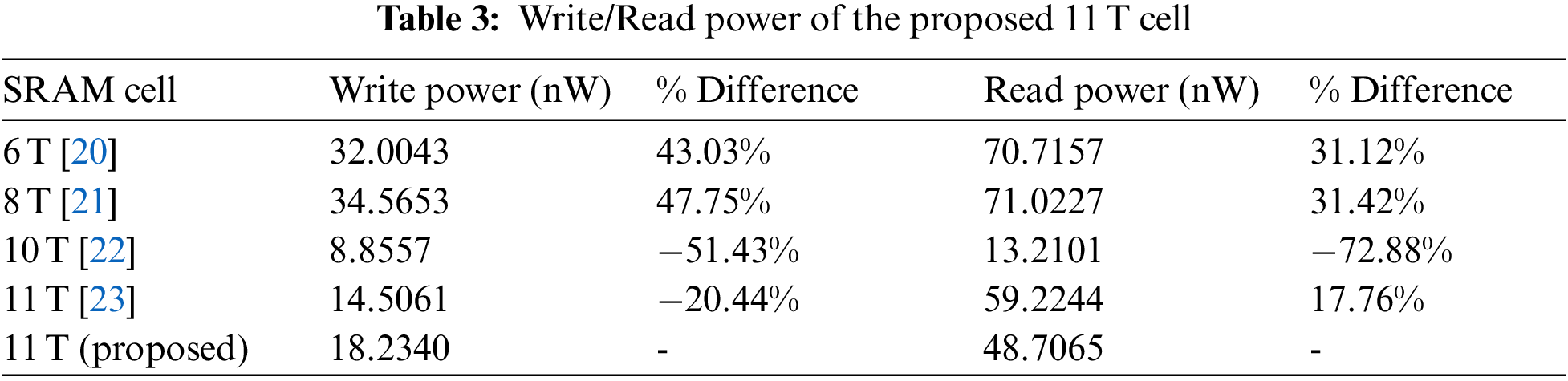
The overall dynamic power consumption of the presented cell and other cells from the literature have been measured during the write and read operations for different frequency range (from 5 to 1 MHz) as plotted in Fig. 7. The proposed 11 T cell consumes an average of 43.55%, 47.75% lower power during write operation compared 6 T and 8 T cells on different frequency with less discharging at output nodes. Similarly, the average read power is also lower by 35.59%, 3.56% and 23.98% over 6 T, 8 T and 11 T cells due to a separate read circuit.
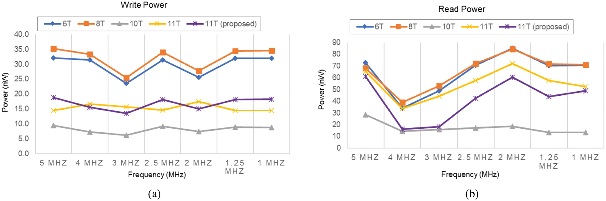
Figure 7: Power of various cells vs. frequency (a) Write operation (b) Read operation
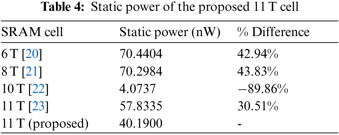
The static power is measured during the hold mode when there is no activity. SRAM memory's static power is a challenge in the idle state due to tremendous increase in leakage current at transition point. It is generally measured when word-line WL and read word-line RWL are at low. The static power of proposed cell is 42.94%, 43.83% and 30.51% lower than 6 T, 8 T and 11 T cells as shown in Tab. 4. The static power is reduced by the stacking effect induced by the tail transistors NM3 and NM4. The power from the memory during the hold mode is defined as the leakage power which has become a major challenge for cache memory on SRAM cells especially in the nano-meter regime.
Another important SRAM design parameter is the current. The write/read current of 11 T cell are investigated and measured at transient time of 1 μs which is presented in Tab. 5. The write current of suggested 11 T cell is less than 6 T and 8 T cells. However, the read current of the 11 T cell is 19.17%, 7.15% and 6.04% more compared to 6 T, 8 T and 11 T cells. The overall current of the 11 T cell and other comparative cells from the literature have been measured during write and read operations for different frequency ranging from 5 to 1 MHz and analyzed. The proposed 11 T cell's average current is 83.29% and 22.01% higher than the 10 T and 11 T cells. The average read current is higher than 6 T cell only. The cell current for write and read mode is plotted in Fig. 8.
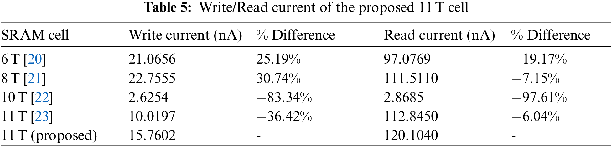
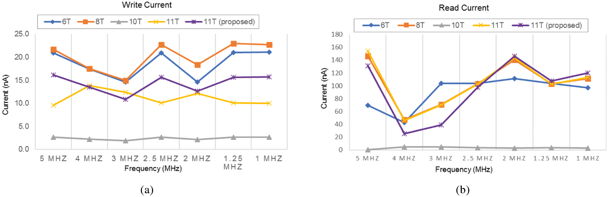
Figure 8: Cell current of various cells vs. frequency (a) Write operation (b) Read operation
4.3.1 Write Delay and Read Delay
The delay or access time is normally used to calculate the speed and performance of the SRAM cell. The write delay is measured between the word line WL and either one output Q or NQ from the first rising or falling edge with 50% threshold voltage. The read delay is measured between the RWL and RBL from the first rising or falling edge with 50% threshold voltage. The delay measured at transient time of 1 μs is presented in Tab. 6. The write delay has improved about 26.46%, 37.16%, 40.19% and 65.02% compared to 6 T, 8 T, 10 T and 11 T cells. It is noted from the results that read delay for 11 T cell is high and recorded as 100.908 ns. The read delay is lowered by 50.64% and 72.90% over 6 T and 10 T cells. The delay time has also been measured at various frequency and shown in Fig. 9.
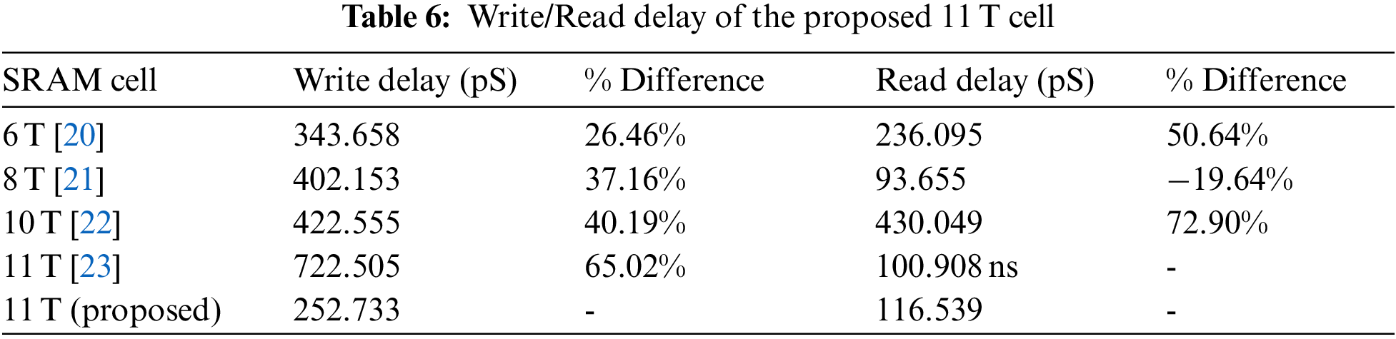
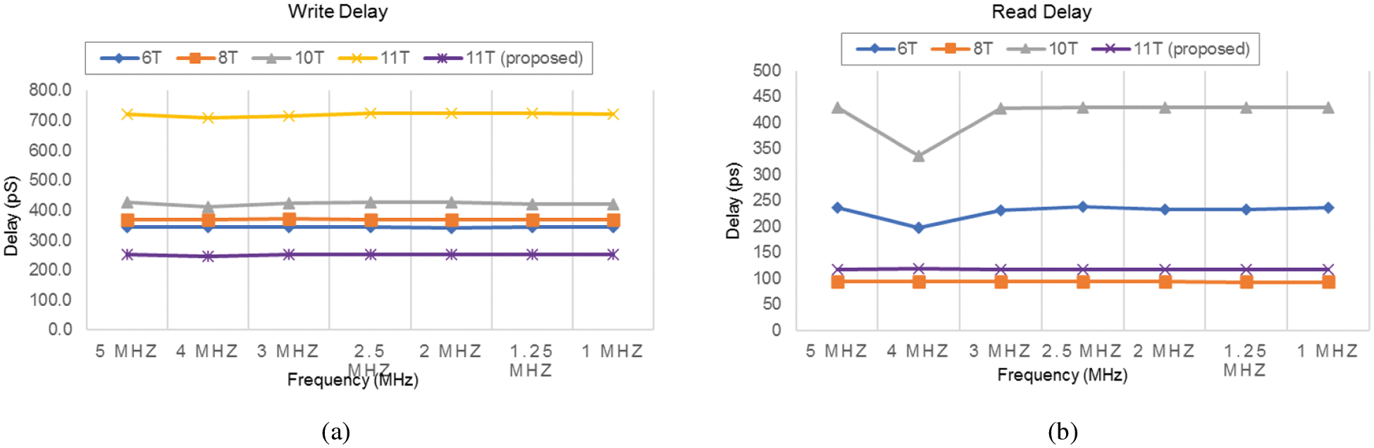
Figure 9: Delay of various cells vs. frequency (a) Write delay (b) Read delay
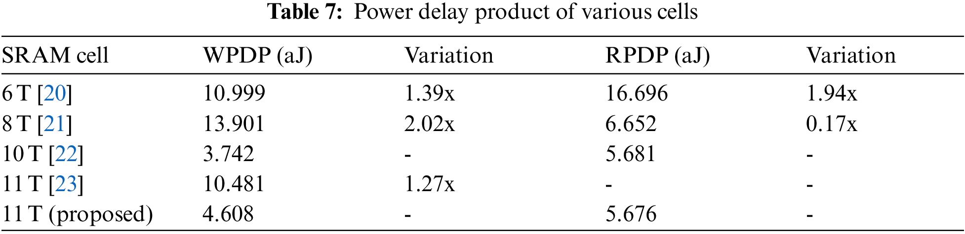
The energy efficiency of SRAM cell is determined by calculating power delay product (PDP) [27]. The product value of delay and the respective power dissipated for write and read operations are known as power delay product. The cell's potential enhancement is also estimated through PDP calculation for both write and read operations. The Write power delay product (WPDP) and Read power delay product (RPDP) are presented in the Tab. 7. It is derived from the results that proposed 11 T cell's write power delay product is lower by 1.39x, 2.02x, 1.27x over 6 T, 8 T, 11 T cells and read power delay product is 1.94x, 0.17x less against 6 T, 8 T cells at 1 V. In general, the delay (time) plays a major role in the PDP calculation. Moreover, the suggested 11 T cell has the lowest write delay which shows the significant reduction of energy consumption. The less power delay product confirms that the proposed cell is energy efficient compared to other cells. Even though 8 T cell with least read delay, yet it is noted higher RPDP due to higher power for read operation.
The stability of suggested and comparative cells has been analyzed in terms of static noise margin (SNM). The minimum DC noise that is needed to switch the stored bit in a node is known as SNM. The SNM is normally measured during hold, read and write operations which are named as Hold static noise margin (HSNM), Read static noise margin (RSNM) and Write noise margin (WNM). It is noted that the SRAM cell robustness can be achieved with higher SNM value for all the operations [28]. The traditional butterfly curve technique is used to calculate the static noise margin in this paper [29].
The HSNM can be defined as the maximum DC voltage that a cell can tolerate without losing data during hold mode. HSNM is measured when bit-lines BL and NBL are connected to VDD (1 V), WL and RWL are connected to the ground (0 V). The HSNM for suggested 11 T, 6 T and 8 T and cells are plotted in Fig. 10. The HSNM of the proposed cell is 400 mV which is nearly equal to other cells.
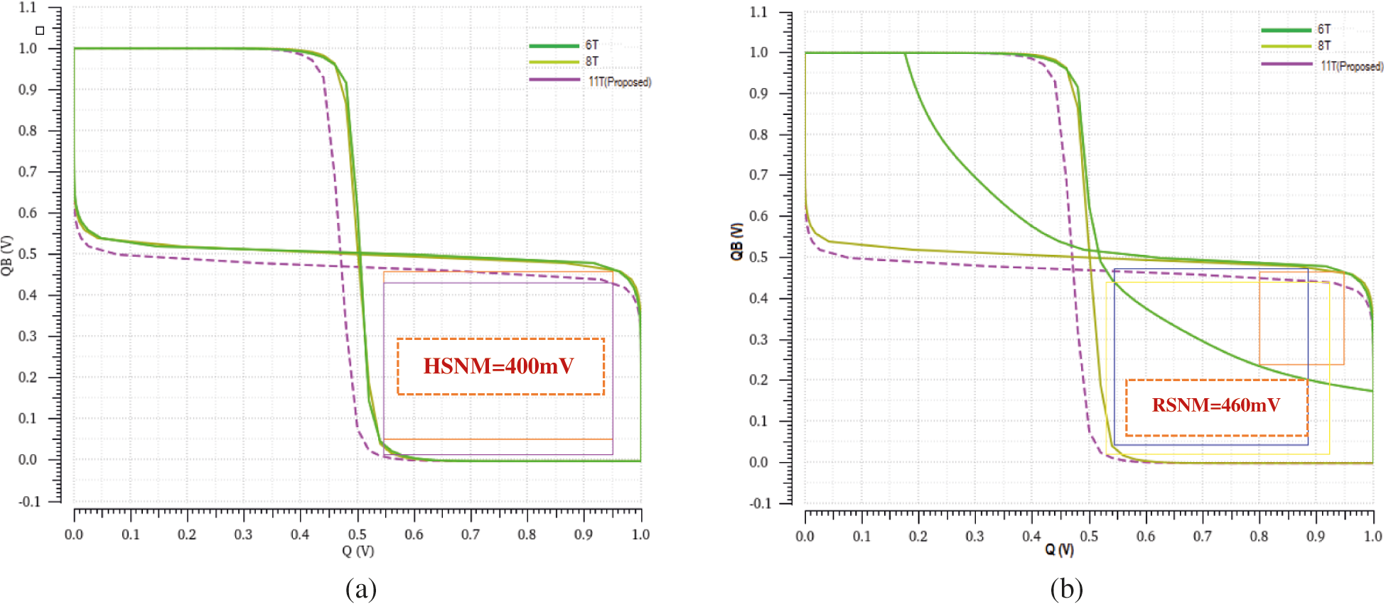
Figure 10: (a) HSNM of 6 T, 8 T and proposed 11 T cells (b) RSNM of 6 T, 8 T and proposed 11 T cells
The read static noise margin is the maximum DC voltage that a cell can tolerate without losing the data in read operation. The RSNM is measured at 1 V supply voltage when bit-lines BL and NBL are connected to VDD (1 V), word-line WL is connected to ground (0 V), RWL are connected to the VDD (1 V) and with RBL precharged. The single ended read circuit with series connected transistors NM5, NM6 and NM7 do not affect the output nodes Q and NQ which results in achieving higher RSNM. The RSNM for 11 T, 6 T and 8 T cells are depicted in Fig. 10. It is calculated that the RSNM of 11 T cell is 460 mV, 8 T is 345 mV and 6 T is 160 mV. It is also evident from the butterfly curve that RSNM of proposed cell is higher and 1.88x and 0.33x improved when compared to 6 T and 8 T cells. The suggested 11 T cell achieves improved read stability.
The write ability of SRAM cell is measured using write noise margin [30,31]. The WNM is calculated at 1 V supply voltage when bit-lines BL and NBL are assigned with 1 and 0 alternatively for write 1 and 0 operations with WL is connected to VDD (1 V) and read word-line RWL is connected to the ground (0 V). The WNM of 6 T, 8 T and proposed 11 T cells are depicted in Fig. 11. It is obvious from the bigger square of 11 T cell and measured that the WNM of the 11 T cell is 450 mV, 8 T cell is 420 mV and for 6 T is 370 mV. The simulation outcome confirms that the WNM of the 11 T cell has 17.78% and 6.67% improvement over 6 T and 8 T cells.
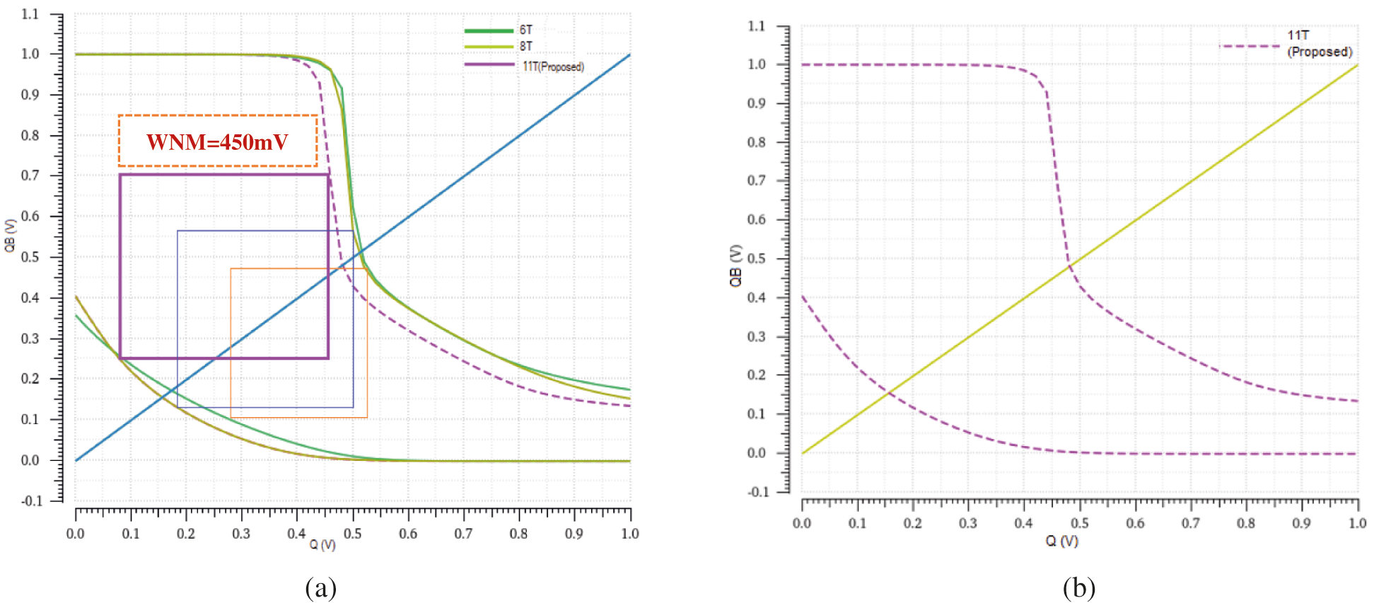
Figure 11: WNM of SRAM cells @ 1 V supply voltage (a) All cells (b) Proposed 11 T cell
4.6.1 Process/Voltage/Temperature Variation
The SRAM cells have severe effect on process variations with power dissipation, speed, performance, and stability [32,33]. The process analysis on all process corners i.e., TT (Typical NMOS, Typical PMOS), FF (Fast NMOS, Fast PMOS), FS (Fast NMOS, Slow PMOS), SF (Slow NMOS, Fast PMOS) and SS (Slow NMOS, Slow PMOS) has been investigated for all the operations. The worst-case variation can be analyzed through corner analysis. The PVT (process, voltage, temperature) variation is performed to determine the propagation time of the transistors. The extreme level of parametric variation can be determined from process corner simulations [34]. The voltage variation is applied from 0.2 V till 1 V to analyze the behavior and performance of cells. The temperature variation is applied from −50°C to 150°C to understand the cell immunity at different environmental conditions.
4.6.2 Impact of PVT Variation on Write Power and Delay
Due to inter-die variations, the threshold voltage will always change. Hence, the power, delay, performance and stability are normally affected [35,36]. The write power and write delay simulation results at all the process corners are reported in Tab. 8. The Figs. 12 and 13 show the voltage and temperature variation for write power and delay. The proposed cell performs better in all the corners compared to other cells and improves the write ability. The proposed cell's average power and delay for write operation is lesser compared to other cells.
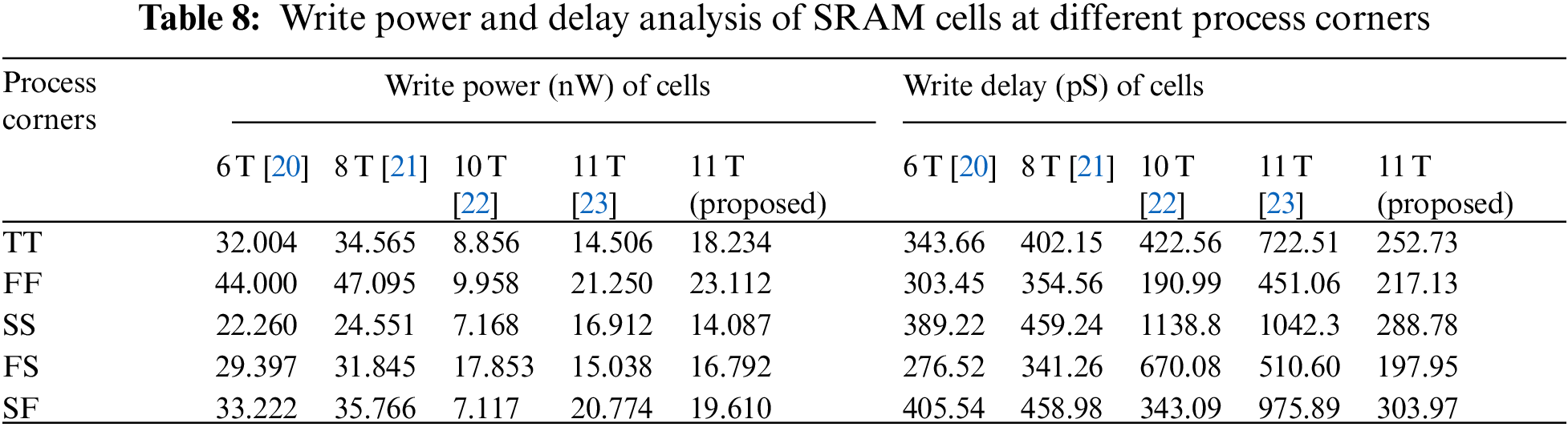
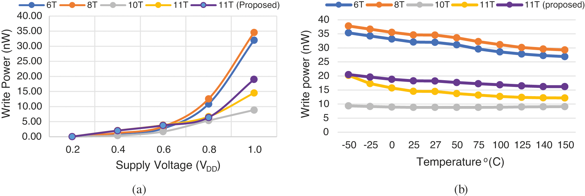
Figure 12: Variation analysis of write power (a) Supply voltage variation (b) Temperature variation
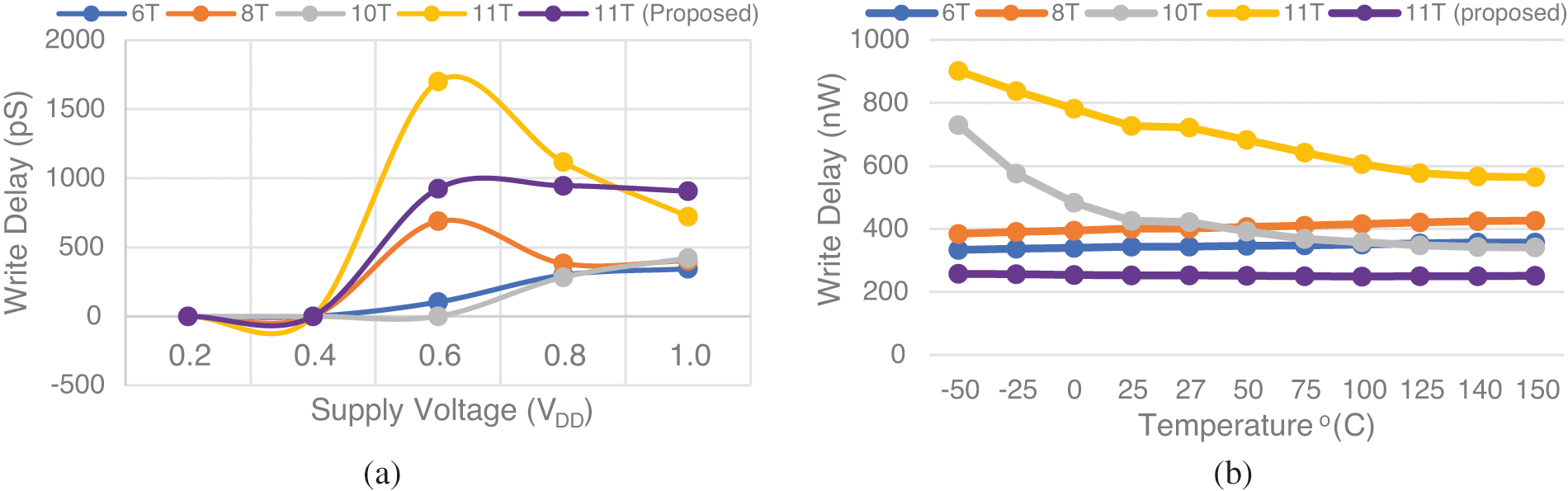
Figure 13: Variation analysis of write delay (a) Supply voltage variation (b) Temperature variation
4.6.3 Impact of PVT Variation on Read Power and Delay
The read power and read delay simulation results at all the process corners are presented in Tab. 9. The voltage and temperature variation results for read power and delay are plotted in Figs. 14 and 15. The proposed cell becomes faster in higher voltages and same time this causes the minimum effect of variation and increases the read stability. The proposed cell is stable and can be used in any suitable environment settings/conditions and perfectly works for VDD as low as 400 mV without any degradation. The average read delay of the suggested 11 T cell is comparatively less and stability is improved in all corners.
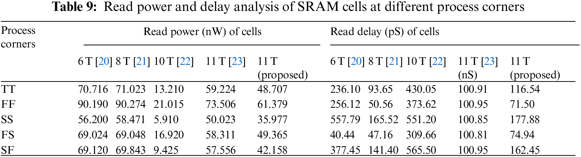
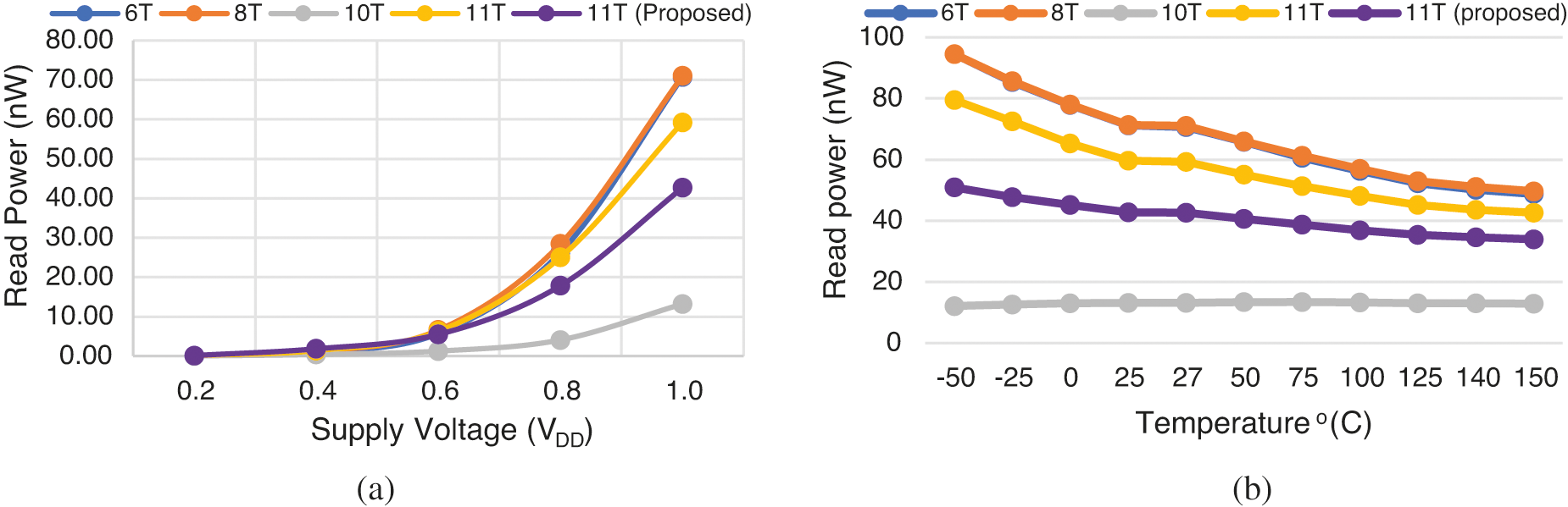
Figure 14: Variation analysis of read power (a) Supply voltage variation (b) Temperature variation
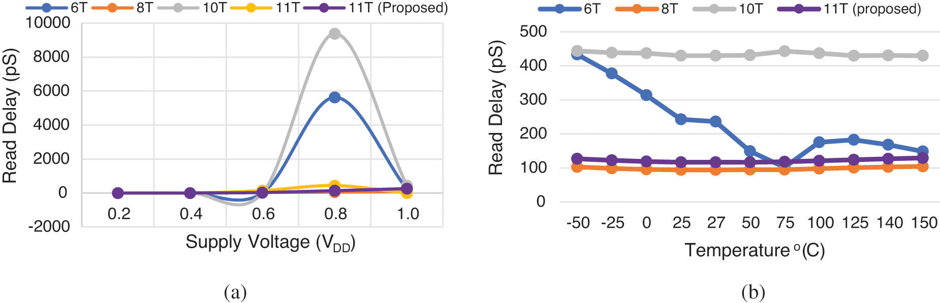
Figure 15: Variation analysis of read delay (a) Supply voltage variation (b) Temperature variation
4.6.4 Impact of PVT Variation on Static Power
The simulation results of static power variations are plotted in Fig. 16. With the increase of temperature, the static power normally increases [37]. The variation of temperature will affect the speed of the cell [38]. The average static power is less compared to other cells in process variation due to the stack effect of the tail transistors. The static power is about 42% less in different temperature variation analysis compared to 6 and 8 T cells.
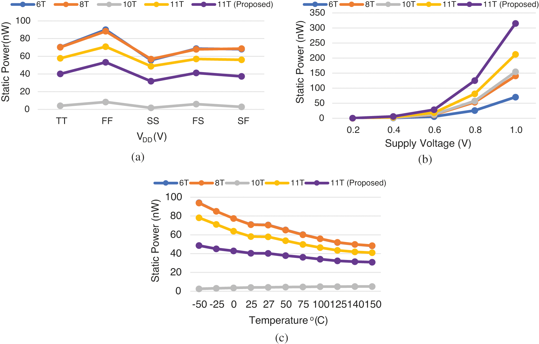
Figure 16: Variation analysis of static power (a) Process corners (b) Supply voltage (c) Temperature
4.7 Statistical Variability Analysis of the Proposed Cell
The Monte Carlo (MC) analysis is carried out to evaluate the proposed cell's effectiveness and robustness at VDD = 1 V for all three operations. The Gaussian distribution with 3σ variation of 10% is applied while carrying out the MC simulation on 5000 samples for all operations. The statistical outcome and distribution for write and read power is plotted in Fig. 17. The mean (μ) and standard deviation (σ) of power and delay with respect to process and mismatch variations are presented in Tabs. 10 and 11. It can be inferred from the table that the mean write power of proposed cell is 42% and 47% less and mean read power is less by 31% over 6 T, 8 T and 18% against 11 T cells. The variability (σ/μ) is also calculated and presented for power and delay of all cells at 1 V.
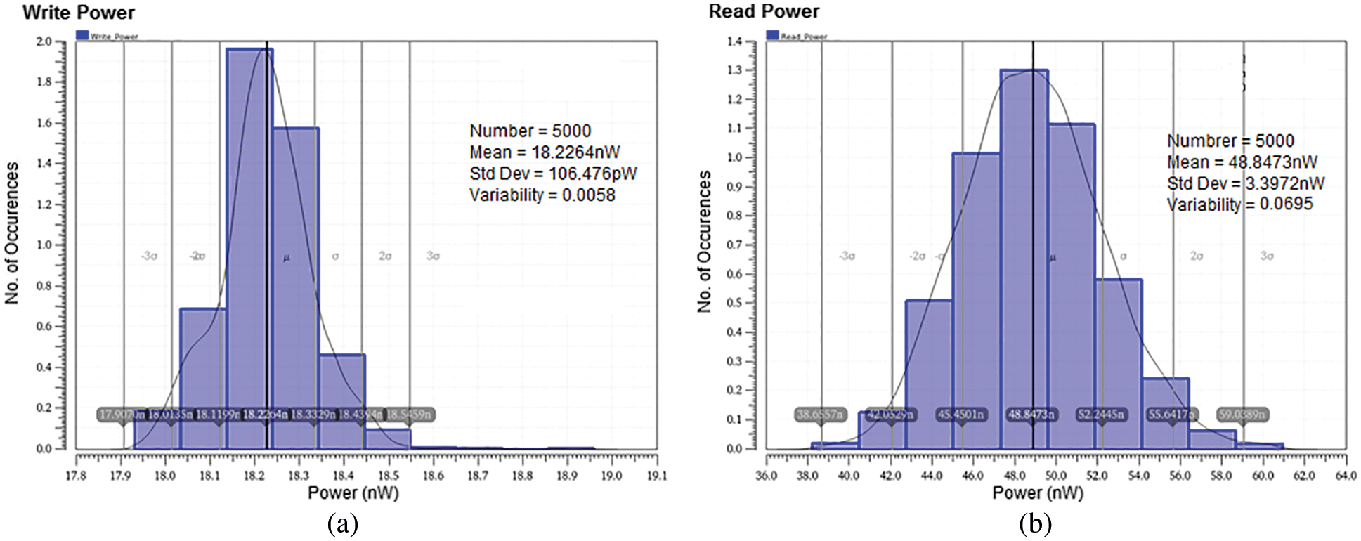
Figure 17: The 5000 MC simulation of proposed cell (a) Write power (b) Read power
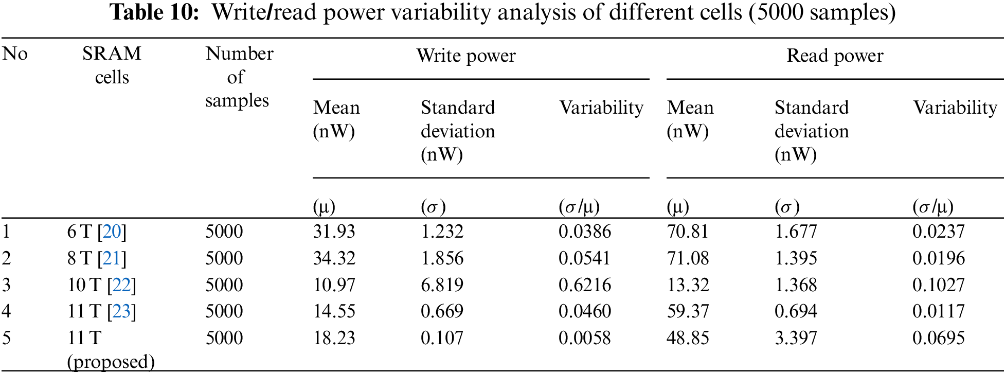
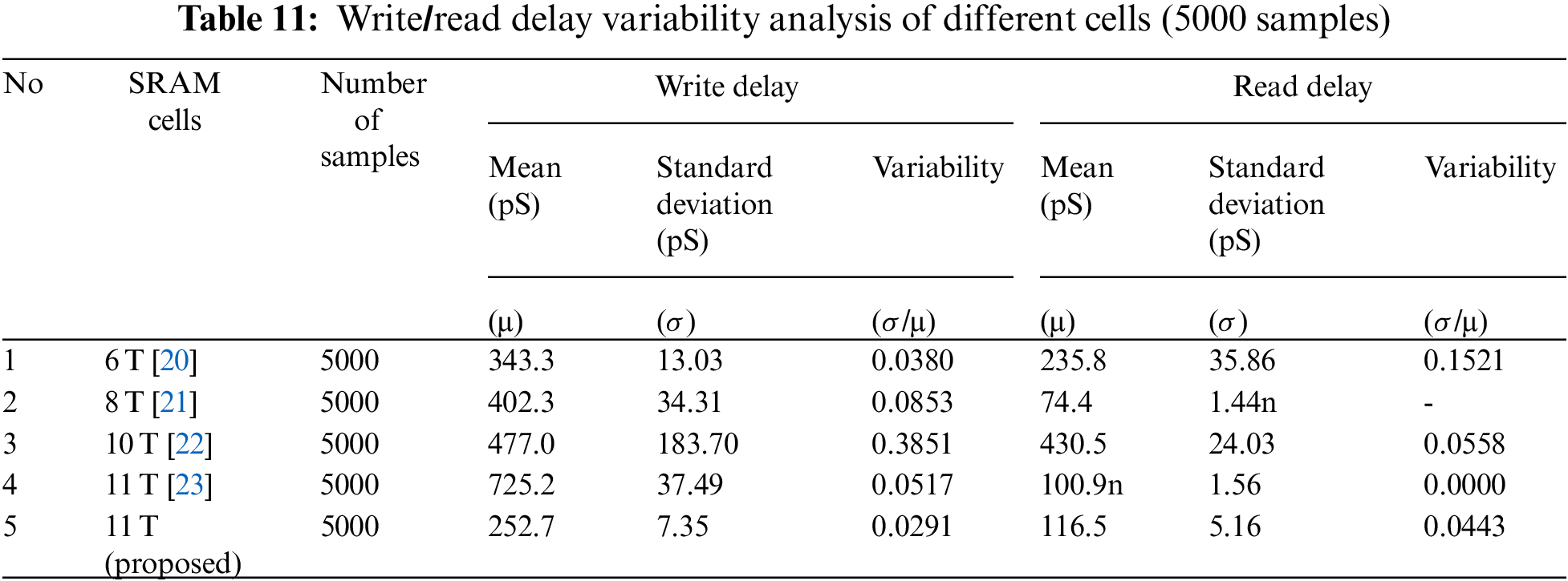
The process tolerance of the cells is evaluated by using the power variability as one main parameter [39,40]. The variability comparison of 11 T and others are presented in Tabs. 10 and 11. It is noted from the table that variability of 11 T cell is 0.0058 for write and 0.0695 for read mode which is significantly less against other cells. Overall, the lower variability (σ/μ) exhibited by proposed cell against other cells on random variation affirms that the cell is robust enough for any suitable applications [41,42].
The Fig. 18 shows the layout of suggested 11 T and 6 T cells drawn in 45 nm CMOS technology with its due design rules. The layouts for all the literature cells have been designed and tested with design rule check (DRC) rules and upon checking layout vs. schematic (LVS) connections, the RC extraction is carried out. The proposed cell exhibits 2.42x area overhead against normalized area of 6 T cell. The other cells show additional area of 1.24x, 1.72x and 1.68x for 8 T, 10 T and 11 T cells.
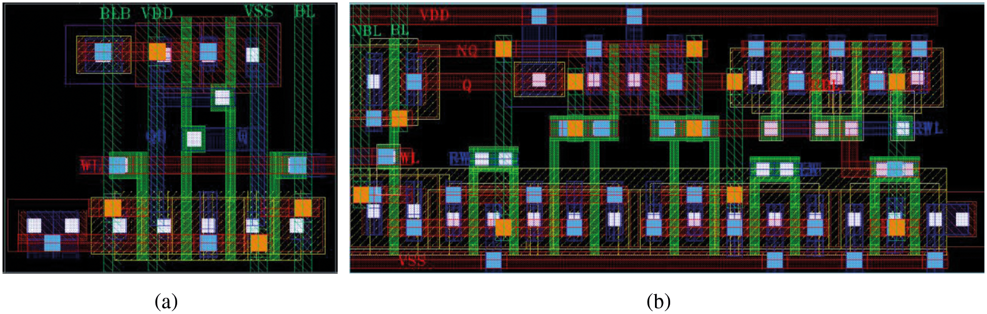
Figure 18: Layout diagram (a) 6 T SRAM cell (b) Proposed 11 T cell
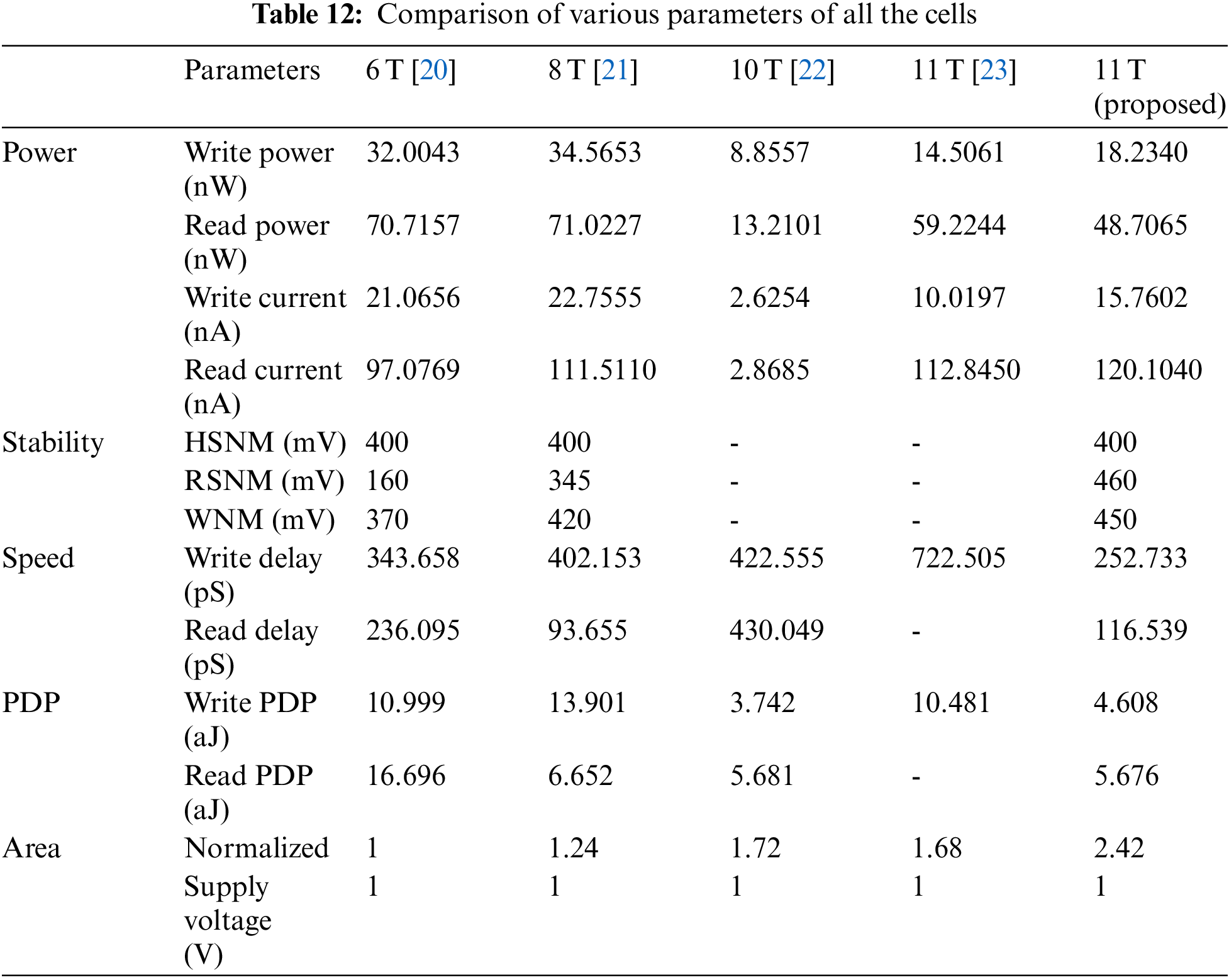
In this research paper, process tolerant and power efficient 11 T SRAM cell is presented and compared with other cells with respect to power, current, delay, stability and area overhead. The cell uses core latch property for write operation and single ended read approach for improving RSNM. The results of various comparative parameters of the cells are summarized in Tab. 12. The WPDP and RPDP are lower by 0.17x, 2.02x and 1.94x, 1.39x against 6 T and 8 T cells that shows the proposed cell is energy efficient with significant process tolerance with variations. The proposed cell is also analyzed in terms of PVT variation as well as MC simulation on 5,000 samples to see the statistical variation. The 0.0058 and 0.0695 variability of the cell for write and read power is less against other cells. The MC simulation and variability analysis outcome validates the efficiency and robustness of the proposed cell without any degradation. The cell exhibits an average lower power of 45%, 33% and improved delay of 32%, 19% for write and read operations over 6 T and 8 T cells in all process corners. The cell also behaves stable at all varying supply voltage and temperature. Thus, PVT analyses affirm that 11 T cell is highly immune to process variation and environmental conditions. In conclusion, the proposed 11 T SRAM cell design is highly appropriate and an ideal choice for Internet of Things applications.
Acknowledgement: The authors would like to acknowledge the support provided by Manipal International University, Malaysia and Multimedia University, Malaysia for this work. The authors would like to thank the editors of CMC and anonymous reviewers for their time and reviewing this manuscript.
Funding Statement: The authors received no specific funding for this study.
Conflicts of Interest: The authors declare that they have no conflicts of interest to report regarding the present study.
1. C. Perera, C. H. Liu, S. Jayawardena and M. Chen, “A survey on internet of things from industrial market perspective,” IEEE Access, vol. 2, pp. 1660–1679, 2014. [Google Scholar]
2. G. Patrick and A. Gattani, Memory Plays a Vital Role in Building the Connected World. Electronic Design, Hong Kong, China, 2015. [Online]. Available: https://www.electronicdesign.com/technologies/iot/article/21800623/memory-plays-a-vital-role-in-building-the-connected-world. [Google Scholar]
3. V. J. Hodge, S. O'Keefe, M. Weeks and A. Moulds, “Wireless sensor networks for condition monitoring in the railway industry: A survey,” IEEE Transactions on Intelligent Transportation Systems, vol. 16, no. 3, pp. 1088–1106, 2015. [Google Scholar]
4. S. M. Kang and Y. Leblebici, “CMOS Digital Integrated Circuits: Analysis and Design,” Second Edition, New York, USA: McGraw-Hill, pp. 402–447, 1996. [Google Scholar]
5. P. Singh, B. S. Reniwal, V. Vijayvargiya, V. Sharma and S. K. Vishvakarma, “Ultra low power-high stability, positive feedback controlled (PFC) 10 T SRAM cell for look up table (LUT) design,” Integration, vol. 62, pp. 1–13, 2018. [Google Scholar]
6. K. Agrawal and S. Nassif, “The impact of random device variation on SRAM cell stability in Sub-90-nm CMOS technologies,” IEEE Transaction on Very Large-Scale Integration, vol. 16, no. 1, pp. 86–97, 2008. [Google Scholar]
7. Y. J. Chang, F. Lai and C. L. Yang, “Zero-aware asymmetric SRAM cell for reducing cache power in writing zero,” IEEE Transactions on Very Large-Scale Integration (VLSI) Systems, vol. 12, no. 8, pp. 827–836, 2004. [Google Scholar]
8. Z. Liu and V. Kursun, “Characterization of a novel nine-transistor SRAM cell,” IEEE Transactions on Very Large Scale Integration (VLSI) Systems, vol. 16, no. 4, pp. 488–492, 2008. [Google Scholar]
9. C. M. R. Prabhu and A. K. Singh, “Novel eight-transistor SRAM cell for write power reduction,” IEICE Electronics Express, vol. 7, no. 16, pp. 1175–1181, 2010. [Google Scholar]
10. S. Ahmad, M. K. Gupta, N. Alam and M. Hasan, “Low leakage single bitline 9 T (SB9 T) static random access memory,” Microelectronics Journal, vol. 62, pp. 1–11, 2017. [Google Scholar]
11. V. Sharma, P. Bisht, A. Dalal, M. Gopal, S. K. Vishvakarma et al., “Half-select free bit-line sharing 12 T SRAM with double-adjacent bits soft error correction and a reconfigurable FPGA for low-power applications,” AEU-International Journal of Electronics and Communications, vol. 104, pp. 10–22, 2019. [Google Scholar]
12. T. H. Kim, H. Jeong, J. Park, H. Kim, T. Song et al., “An embedded level-shifting dual-rail SRAM for high-speed and Low-power cache,” IEEE Access, vol. 8, pp. 187126–187139, 2020. [Google Scholar]
13. S. Pal and A. Islam, “9-T SRAM cell for reliable ultralow-power applications and solving multibit soft-error issue,” IEEE Transactions on Device and Materials Reliability, vol. 16, no. 2, pp. 172–182, 2016. [Google Scholar]
14. S. Pal, S. Bose, W. H. Ki and A. Islam, “Characterization of half-select free write assist 9 T SRAM cell,” IEEE Transactions on Electron Devices, vol. 66, no. 11, pp. 4745–4752, 2019. [Google Scholar]
15. R. Lorenzo and R. Pailly, “Single bit-line 11 T SRAM cell for low power and improved stability,” IET Computers & Digital Techniques, vol. 14, no. 3, pp. 114–121, 2020. [Google Scholar]
16. A. Islam and M. Hasan, “A technique to mitigate impact of process, voltage, temperature variations on design metrics of SRAM cell,” Microelectronics Reliability, vol. 52, no. 2, pp. 405–411, 2012. [Google Scholar]
17. H. Yang, J. Hu and H. Zhu, “Novel SRAM cells using dual-threshold independent gate FinFETs,” in IEEE 17th Int. Conf. on Nanotechnology (IEEE-NANO), Pittsburgh, PA, USA, pp. 358–359, 2017. [Google Scholar]
18. V. Sharma, M. Gopal, P. Singh, S. K. Vishvakarma and S. S. Chouhan, “A robust, ultra-low-power, data-dependent power supplied 11 T SRAM cell with expanded read/write stabilities for internet-of-things applications,” Analog Integrated Circuits and Signal Processing, vol. 98, no. 2, pp. 331–346, 2019. [Google Scholar]
19. P. S. Grace and N. M. Sivamangai, “Design of 10 T SRAM cell for high SNM and Low power,” in Third Int. Conf. on Devices, Circuits and Systems (ICDCS ‘16), Coimbatore, India, pp. 281–285, 2016. [Google Scholar]
20. N. Rahman and B. P. Singh, “Static-noise-margin analysis of conventional 6 T SRAM cell at 45 nm technology,” International Journal of Computer Applications, vol. 66, no. 20, pp. 19–23, 2013. [Google Scholar]
21. H. Noguchi, S. Okumura, Y. Iguchi, H. Fujiwara, Y. Morita et al., “Which is the best dual-port SRAM in 45-nm process technology-8 T, 10 T single end, and 10 T differential,” in Proc. of IEEE Int. Conf. on Integrated Circuit Design and Technology, (IEEE ICICDT), Grenoble, France, pp. 55–58, 2008. [Google Scholar]
22. G. Prasad, N. Kumari, B. P. Mandi and M. Ali, “Design and statistical analysis of low power and high speed 10 T static random access memory cell,” International Circuit Theory Applications, vol. 48, no. 8, pp. 1319–1328, 2020. [Google Scholar]
23. V. Sharma, N. Gupta, A. P. Shah, S. K. Vishvakarma and S. S. Chouhan, “A reliable, multi-bit error tolerant 11 T SRAM memory design for wireless sensor nodes,” Analog Integrated Circuits and Signal Processing, vol. 107, no. 2, pp. 339–352, 2021. [Google Scholar]
24. E. Grossar, M. Stucchi, K. Maex and W. Dehaene, “Read stability and write-ability analysis of SRAM cells for nanometer technologies,” IEEE Journal of Solid-State Circuits, vol. 41, no. 11, pp. 2577–2588, 2006. [Google Scholar]
25. T. G. Sargunam, C. M. R. Prabhu and L. W. Soong, “A robust, high performance and Low power (HPLP) 8 T SRAM cell for IoT applications,” International Journal of Scientific & Technology Research, vol. 9, no. 11, pp. 330–337, 2020. [Google Scholar]
26. C. M. R. Prabhu, T. G. Sargunam and A. K. Singh, “High performance data aware (HPDA) SRAM cell for IoT applications,” ARPN Journal of Engineering and Applied Sciences, vol. 14, no. 1, pp. 91–94, 2019. [Google Scholar]
27. P. Sanvale, N. Gupta, V. Neema, A. P. Shah and S. K. Vishvakarma, “An improved read-assist energy efficient single ended P-P-N based 10 T SRAM cell for wireless sensor network,” Microelectronics Journal, vol. 92, no. 104611, pp. 1–9, 2019. [Google Scholar]
28. S. Pal and A. Islam, “Variation tolerant differential 8 T SRAM cell for ultralow power applications,” IEEE Transactions on Computer Aided Design Integrated Circuits Systems, vol. 35, no. 4, pp. 549–558, 2015. [Google Scholar]
29. C. Duari and S. Birla, “Low leakage SRAM cell with improved stability for IoT applications,” Procedia Computer Science, vol. 171, pp. 1469–1478, 2020. [Google Scholar]
30. K. Takeda, H. Ikeda, Y. Hagihara, M. Nomura and H. Kobatake, “Redefinition of write margin for next-generation SRAM and write-margin monitoring circuit,” in 2006 IEEE Int. Solid-State Circuits Conf.-Digest of Technical Papers (IEEE 2006), San Francisco, CA, USA, pp. 2602–2611, 2006. [Google Scholar]
31. N. Gierczynski, B. Borot, N. Planes and H. Brut, “A new combined methodology for write margin extraction of advanced SRAM,” in 2007 IEEE Int. Conf. on Microelectronic Test Structures (IEEE 2007), pp. 97–100, 2007. [Google Scholar]
32. A. Naghizadeh and M. Gholami, “Two novel ultra-low-power SRAM cells with separate read and write path,” Circuits, Systems, and Signal Processing, Bunkyo-ku, Japan, vol. 38, no. 1, pp. 287–303, 2019. [Google Scholar]
33. S. K. Saha, “Compact MOSFET modeling for process variability-aware VLSI circuit design,” IEEE Access, vol. 2, pp. 104–115, 2014. [Google Scholar]
34. S. Gupta, K. Gupta and N. Pandey, “A 32-nm subthreshold 7 T SRAM bit cell with read assist,” IEEE Transactions on Very Large Scale Integration (VLSI) Systems, vol. 25, no. 12, pp. 3473–3483, 2017. [Google Scholar]
35. P. Singh and S. K. Vishvakarma, “Ultra-low power, process-tolerant 10 T (PT10 T) SRAM with improved read/Write ability for internet of things (IoT) applications,” Journal of Low Power Electronics and Applications, vol. 7, no. 3:24, pp. 1–22, 2017. [Google Scholar]
36. A. Islam and M. Hasan, “A technique to mitigate impact of process, voltage and temperature variations on design metrics of SRAM cell,” Microelectronics Reliability, vol. 52, no. 2, pp. 405–411, 2012. [Google Scholar]
37. N. Gupta, A. P. Shah, S. Khan, S. K. Vishvakarma, M. Waltl et al., “Error-tolerant reconfigurable VDD 10 T SRAM architecture for IoT applications,” Electronics 2021, vol. 10, no. 14:1718, pp. 1–16, 2021. [Google Scholar]
38. A. Sachdeva and V. K. Tomar, “Design of low power half select free 10 T static random-access memory cell,” Journal of Circuits, Systems, and Computers, vol. 30, no. 4:2150073, pp. 1–32, 2021. [Google Scholar]
39. S. Mansore and R. Gamad, “A data-aware write-assist 10 T SRAM cell with bit-interleaving capability,” Turkish Journal of Electrical Engineering and Computer Sciences, vol. 26, no. 5, pp. 2361–2373, 2018. [Google Scholar]
40. A. Sachdeva and V. K. Tomar, “Design of 10 T SRAM cell with improved read performance and expanded write margin,” IET Circuits, Devices & Systems, vol. 15, no. 1, pp. 42–64, 2020. [Google Scholar]
41. K. Yu, L. Tan, S. Mumtaz, S. Al-Rubaye, A. Al-Dulaimi et al., “Securing critical infrastructures: Deep- learning-based threat detection in IIoT,” IEEE Communications Magazine, vol. 59, no. 10, pp. 76–82, 2021. [Google Scholar]
42. L. Zhen, Y. Zhang, K. Yu, N. Kumar, A. Barnawi et al., “Early collision detection for massive random access in satellite-based internet of things,” IEEE Transactions on Vehicular Technology, vol. 70, no. 5, pp. 5184–5189, 2021. [Google Scholar]
 | This work is licensed under a Creative Commons Attribution 4.0 International License, which permits unrestricted use, distribution, and reproduction in any medium, provided the original work is properly cited. |