DOI:10.32604/cmc.2022.025931
| Computers, Materials & Continua DOI:10.32604/cmc.2022.025931 | |
| Article |
Flexible Memristive Devices Based on Graphene Quantum-Dot Nanocomposites
Department of System Semiconductor Engineering, SangMyung University, Cheonan-si, 31066, Korea
*Corresponding Author: Dae-Ki Hong. Email: hongdk@smu.ac.kr
Received: 09 December 2021; Accepted: 16 February 2022
Abstract: Artificial neural networks (ANNs) are attracting attention for their high performance in various fields, because increasing the network size improves its functioning. Since large-scale neural networks are difficult to implement on custom hardware, a two-dimensional (2D) structure is applied to an ANN in the form of a crossbar. We demonstrate a synapse crossbar device from recent research by applying a memristive system to neuromorphic chips. The system is designed using two-dimensional structures, graphene quantum dots (GQDs) and graphene oxide (GO). Raman spectrum analysis results indicate a D-band of 1421 cm−1 that occurs in the disorder; band is expressed as an atomic characteristic of carbon in the sp2 hybridized structure. There is also a G-band of 1518 cm−1 that corresponds to the graphite structure. The G bands measured for RGO-GQDs present significant GQD edge-dependent shifts with position. To avoid an abruptly-formed conduction path, effect of barrier layer on graphene/ITO interface was investigated. We confirmed the variation in the nanostructure in the RGO-GQD layers by analyzing them using HR-TEM. After applying a negative bias to the electrode, a crystalline RGO-GQD region formed, which a conductive path. Especially, a synaptic array for a neuromorphic chip with GQDs applied was demonstrated using a crossbar array.
Keywords: Memristive devices; neuromorphic chip; resistive RAM; quantum dot; graphene
Recently, the von Neumann method of implementing the existing serial processing structure has been found to have performance limitations in memory and computing system processing due to the functionally limited memory access process and bottlenecks of processed information. To overcome these performance limitations, over the past few years, artificial neural networks (ANNs) have made significant progress in many fields, such as image processing [1–5] and object recognition [6–13]. However, the performance of ANNs is significantly new heterogeneous parallel device structures that enable computational performance can be alternatives. This area of research involves the development of flexible devices, which enable many exciting applications, from big data processing capacity to image analysis; deep neural networks (DNNs) have also been tried in various structures recently [14,15]. However, the complex circuit structure and large power consumption needed to increase the performance limits device use in various embedded-type applications [16,17]. The use of a memristive device is widely regarded as a hardware-implemented system solution, using an internal memory circuit in a deep neural network based on a parallel architecture.
As such, the implementation of a new heterogeneous structure-based device can completely avoid unnecessary noise and leakage current in the circuit [18–20]. In particular, the advent of new memory technologies, such as resistive technology, which have emerged as real alternatives, make it possible to maximize the performance of next-generation random access memory (RRAM) structures [21,22]. Until recently, breakthrough technologies were realized through innovative structures providing small-area, high-speed, nonvolatile memory circuits applicable to Complementary Metal Oxide Semiconductor (CMOS) network systems [23]. However, Parallel heterogeneous neuromorphic engineering applies CMOS-based digital-analog Very Large Scale Integration (VLSI) to realize high-performance and flexible ANNs [24]. For resistive memory, various geometries of devices have been used to engineer memristive devices and integrate them into crossbar structures [25]. Therefore, to take full advantage of the parallel structure, a continuous hardware configuration is essential to integrate crossbar array integrated memory devices with CMOS technology.
In particular, memristors have advantages as next-generation storage devices due to their high power density and low power consumption, and their flexible structures [26]. A passive two-terminal memristor is a primary electronic device with a built-in synaptic nonvolatile memory function in an array-structure crossbar. Various studies have reported on the design of a heterostructure of the active layer that controls the spatial resolution and resistive memory properties of crossbar ion channel electrodes [27]. A memristor is a passive two-terminal structure element composed of a metal layer that supplies carriers and a dielectric layer where ion channels form. The physical mechanism is important in forming conductive filaments (CF), which serve as ion paths at the interface between the metal contact and the active layer [28]. In the case of a formation of a CF between electrodes when oxygen vacancy occurs in the metal oxide layer by an externally applied voltage, a filament forms by penetration of the electrode metal material into the oxide film due to electrical stress [29]. The CFs formed in this way repeat the generation and rupture of the filament path according to the magnitude or direction of the voltage, and the resistance value changes.
Device has a memory characteristic of having high resistance (OFF state) at a low voltage and a low resistance (On state) at a specific voltage. Rapid changes in resistive memory occur depending on the structure used in the device and the way the conductive channels are implemented. After CF formation via voltage application the memristor unit can perform a reversible transition between the high-resistance state (HRS) and the low-resistance state (LRS). The reversible conversion operation from HRS to LRS is controlled through a set process. On the other hand, the reversible conversion operation from LRS to HRS is controlled through a reset process. The crossbar array-based neuron structure implements the calculation function of the weight value, which is the main parameter of the synaptic device [30]. Therefore, considering these fundamental physical performance limitations, because it is no longer possible to narrow the desired level gap compared to the latest technology via device expansion alone, a crossbar array synaptic device with a new structure can be an alternative [31].
The physical properties, such as the van der Waals force of low-dimensional materials, are important in constructing a resistive memory with a new structure [32]. Among low-dimensional structures, we focused on graphene quantum dots (GQDs) and reduced graphene oxide (RGO), which can control quantum effects and effective mass, and have advantages not only as novel active layers but also as flexible electrical device applications [33]. GQDs are two-dimensional planar nanoflakes with thicknesses of a few atomic layer; they are defect-free and have dominant size and edge properties [34]. GQDs can be applied as active layers in crossbar structures, enabling the implementation of next-generation RRAM. GQD-based CF formation characteristics are consistent, and reproducible performance is possible.
The Strukov's research team at the University of California Santa Barbara developed an ANNs using a 12 × 12 array of resistive memristors [35]. As the iteration of the algorithm increased, the number of misclassified patterns tended to approach zero. Although ANNs using memristors have shown some performance in synaptic operation, problems with neuromorphic circuits are appearing due to high error rates. This is due to the unstable structure of the filament path and structural defects, and the low on/off conversion rate. Recently, artificial synaptic structures designed with inorganic and organic materials showed different results by applying atomic vacancies and interfacial trap principles based on metal and oxide layers. In this work, we demonstrate a parallel-structured memristive crossbar array based on GQDs and GO, without the need for additional passive devices.
2.1 Preparation of Graphene Quantum Dots
Graphene was synthesized on Cu foil in a thermal furnace at 950°C for 7 min under Ar: H2: CH4 mixed-gas flow. Subsequently, a pre-prepared poly (methyl methacrylate) (PMMA, Sigma Aldrich) solution was dropped all over the graphene surface, spincoated at 5000 rpm for 45 s, and then heat treated on a hot plate at 160°C for 3 min. The PMMA solution was prepared by adding 0.5 g PMMA powder to 15 mL chlorobenzene (Sigma Aldrich) and stirring the mixture at 65°C for 8 h. The Cu was removed by dipping the PMMA/graphene/Cu foil stack in 1 M FeCl3 solution (Sigma Aldrich). The PMMA/graphene stack was then transferred onto glass or PET substrate and heat-treated at 110°C for 3 h. Finally, the PMMA was dissolved by acetone. The following processes were used to fabricate GQDs. Graphene oxide (GO) was prepared from graphite powder using the Hummers method. GO was deoxidized in a horizontal furnace at 350–450°C for four hours under Ar to produce reduced graphene oxide powder. About 5.0–6.5 g of graphene oxide powder was oxidized by ultrasonication in concentrated 15 mL H2SO4 and 40 mL HNO3 for 20 h. In addition, 350 mL deionized water was used to dilute the mixture. After cooling to room temperature, the resulting powder was redispersed in 35-mL DI water for two hours under ultrasonication. Then, by filtering the resulting suspension through a 200-nm nanoporous membrane, a brown solution was separated. Since the colloidal solution still contained some large graphene nanoparticles (<200 nm) emitting weak blue fluorescence, it was further filtered overnight in a dialysis bag with a cutoff of 3500 Da molecular weight, thereby producing strongly fluorescent GQDs. The GQDs were separated into different sizes using several dialysis bags of 1000–50,000 Da and a 20-nm nanoporous membrane [36].
To fabricate RRAM-based synapse devices, after the direct synthesis of the extracted GQD and RGO, graphene quantum dots of each shape were directly grown on patterned transparent electrodes on a Cu thin films through a modified CVD method. After washing the composite GQD layer in a deionized water cleaning process, heat treatment was performed. The solution used to establish the dielectric structure of RGO was prepared by sonication of 2.5–7.5 wt% RGO in 2-propanol for 60 min to prepare five samples with different RGO concentrations. The solution was spin coated at 5500 rpm for 35 s to obtain a ∼55 nm thick RGO layer. A cross-bar type Au/RGO GQD/Au/graphene structure was deposited on an ITO substrate by thermal evaporation using a 150 μm wide overlapping hard mask. The coated substrate was heat-treated at 80°C for 10 min to finally obtain the RGO/GQDs layer, which was then cooled to room temperature. Finally, Au metal was thermally evaporated on the RGO/GQDs layer to form the contact. The active areas of all the devices were defined using a shadow mask of 15 mm2.
The surface roughness of the graphene and RGO layers was measured using an atomic force microscope in non-contact mode (AFM, Park Systems, model XE-100). Plane- and cross-sectional-view images of the materials and devices were obtained by field emission scanning electron microscopy (FE-SEM, Carl Zeiss, model LEO SUPRA 55). Morphologies of GQDs were analyzed using an HRTEM (High-resolution Transmission Microscopy) (FEI Tecnai F30 S-Twin). To make the HRTEM specimens, the GQDs were dispersed in DI water, drops of which were then put on C- or SiO-coated Cu grids (Tedpella, Inc., Redding, CA, USA) and mica substrate, respectively. The current-voltage (I–V) curve of the device was analyzed using an electrical and electronic workstation (Keithley 2400). Current density-voltage (J-V) characteristics were monitored by forward/reverse scans at 200 ms and 10 mV under standard conditions. Bending test of the flexible devices was conducted at a 0.5 Hz frequency.
3.1 RRAM-Based Synapse Devices for Neuromorphic Systems
The characteristic of increasing the amount of current according to the frequency with which bias is applied to the memory resistor electrode is similar to that of the synapse that controls the amount of current according to the spike stimulus [37]. From the background of the neuromorphic crossbar system, the computational performance of the synaptic capability is capable of parallel structure-based signal processing [38]. Responses to increases in activity can be mimicked by the proposed resistive memory by reinforcement and depression of the conductance value by proper bias pulses [39]. To show that the RGO-GQDs nonvolatile (NV) random-access devices provided consistent performance as an artificial neural system capable of implementing spike signal output improvement, a 20 ns pulse signal designed to increase in amplitude was used to modulate the resistance change of the RRAM, memristor with properties similar to those of synapses were incorporated into the integrated circuits.
Since the resistance-variable memristor has a structure of two electrodes and an oxide film located between them, it has high resistance (OFF state), and has a memory characteristic having low resistance (On state) from a specific voltage. The rapid change in resistance is related to the microstructure used in the device, and typically appears in two ways. First, with an externally applied potential difference, oxygen vacancies form at the interlayer with a defect between the terminal and the oxide layer. A conductive filament forms through both electrodes [40]. In the second case, the electrode metal material penetrates the oxide layer via electrical stress to form a filament [41]. The channels formed in this way repeat the generation and rupture of the filament according to the magnitude or direction of the potential difference and the resistance changes. In principle, the memristor can persistently store an amount of current that has previously passed by controlling the amount of current and maintaining the charge transfer path between the two even if no voltage is applied in the middle [42].
A 10 nm thick RGO-GQD layer was designed on a Gr/ITO/PI substrate by spray coating method; its structure, confirmed by the high-resolution transmission electron microscopy (HR-TEM), is shown in the image Fig. 1. This layer consists of empty space between GQDs. Defects are negatively biased by oxygen ion diffusion and accumulation in the composite RGO structure, which is associated with the formation of defects. A CF of an active layer based on the resistive memory structure with Au electrode was applied to prevent the destruction of an electric current of 15 μA and prevent the permanent destruction of the electrode. The TE/RGO-GQDs/BE layers indicate stable resistive switching behavior without defect-related bubble formation. Therefore, by applying a negative voltage through the electrode, the electrical resistance increases rapidly at the positive minimum turn-on voltage.

Figure 1: Schematic of synaptic transmission in neural system and illustration of RRAM-based bionic neural cell
The structure of a convolutional neural network with excellent performance in image classification will be briefly reviewed [43]. In addition, a neuromorphic architecture that mimics the human brain and a compression technique that can reduce the number of weight parameters of the neural network are examined. The convolution layer extracts a feature map by conducting convolution calculation of the input image. The convolution operation involves constant size and weights. The kernel with the previously determined parameters extracts features by multiplying and adding parameters corresponding to pixel values while moving the input image [44].
After going through the convolution and weight layers, the stably connected process is performed. A fully connected layer is a structure in which each input node is associated with the complete nodes of the next function. The fully connected layer receives as input features extracted from the convolutional layer and classifies them into objects. After passing through the stably placed layer, the objects are finally output as probability values. A convolutional layer has several parameters but a large amount of computation, and a connection layer has several parameters, but a large amount of computation.
Atomic-scale RGO-GQD layers were designed on a Gr/ITO/PI substrate; these are shown in a schematic of the synaptic transmission in the conductive path, in Fig. 2. RGO-GQD layers structured with several oxygen-functional groups are formed between the top and bottom contacts. Au ions in the bottom electrode penetrate to the Gr of the crystal layer at an initial step of the set process, and these terminal ions create conductive Au/Gr interface defects. This forming of locally conductive paths on the RGO composite layer is a significant phenomenon.

Figure 2: Pattern recognition with neural network using multilayer perceptron algorithm
3.2 Memristive Devices Based on RGO Nano-sheet Nanocomposites
Device was fabricated on a single-layer Gr on an ITO substrate through chemical vapor deposition (CVD); device formation is confirmed in the schematic of the synaptic crossbar in the conductive layers with Gr, as shown in Fig. 3. To prepare the graphene layer for the RGO-GQD RRAM component, through the hard mask, a part of the RGO-GQD layer, and the substrate under the Au layer, were etched down to ∼10 nm, completing the 3D device structure. Then, a GQD layer was formed on the RGO layer by spray coating, and 15 nm of Au was deposited by electron beam deposition to form an electrode for carrier supply. Subsequently, the configuration of the RRAM device with the RGO-GQD active layer was coated with several layers of GQD pieces, on the top and on the memory switching layers. Then, an additional array layer was completed by sputtering of a metal layer on top of the RGO-GQDs by e-beam deposition and lift-off process. Before evaluating the electrical properties, we improved the electrical contact properties. We removed the residual contaminant particles introduced during RGO-GQD coating by annealing the fabricated device at 110°C for 4 h in an H2 carrier gas atmosphere.

Figure 3: Fabrication process flow and schematic device architecture based on Au/RGO-GQDs/Au/graphene/ITO/PI
The stress generated during device fabrication was relieved through the annealing process, and contaminants and moisture were removed to improve the interlayer adhesion in the structure. To electrically connect a resistive memory device having a flexible structure to an electric circuit, a wire bonding process was performed on an electrode supplying a carrier to the active layer.
Chemically induced GO has a unique set of properties resulting from oxygen functional groups introduced via chemical exfoliation of graphite. The thickness of GQDs is 0.34 nm, as measured by atomic force microscopy (AFM). GQDs with sizes of 5 to 10 nm consist of a single layer and exhibited a bilayer structure in localized areas. GQDs were also measured and found to have average height, as shown in Fig. 4a; they were imaged using AFM in contact mode to determine the number of graphene layers. The GQD particles were measured and found to have a height distribution between 0.5 and 3.5 nm on the RGO substrate. The highest part of the GQDs was measured at 1.3 nm. This corresponds to a single graphene layer there were uniform properties inside the RGO layers synthesized by other methods. Raman spectrum analysis indicated a D-band of 1357 cm−1 that occurs in areas of disorder, expressed according to the atomic characteristic of carbon in the sp2 hybridized structure, and a G-band of 1596 cm−1 that corresponds to the graphite structure.
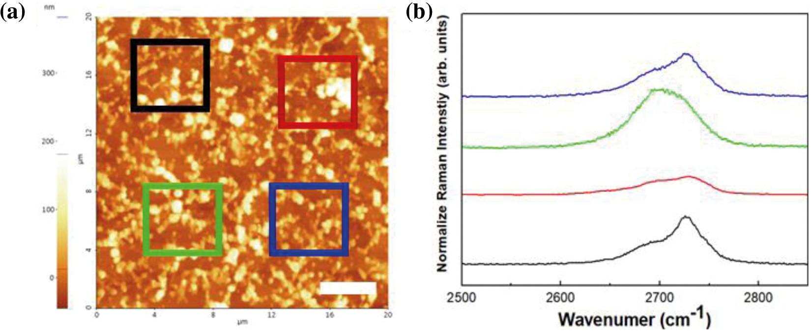
Figure 4: Characterization of chemical state in GQD layers in pristine Raman intensity ratio maps of 2D bands. (b) Raman profiles of black, red, green and blue boxes in (a)
The centers of widely distributed bands at 2690 and 2760 cm−1 correspond to the 2D and D + G bands, respectively, as shown in Fig. 4b. The ratio of D-to-G band intensity changed according to the composition of the RGO-GQD region due to the diffusion of oxygen ions; analysis of the relative intensities of the D bands showed that hexagonal networks of defective carbon atoms were reduced because interatomic stresses were generated as carbon atoms recombine with oxygen-containing groups. It was confirmed that a strong electric field generated conduction channels locally in the composite RGO-GQD region.
Fig. 5 shows Raman spectra of GQDs to indicate chemical states in the GQD layers, the ON and the OFF states, and RGO-GQD/Au/Gr/ITO substrate. The Raman spectrum of the GQDs resolves into two distinctive D and G bands at ∼1421 and ∼1518 cm−1, respectively. The D and G bands hardly move even when the ON and OFF states, which are the devices electrical states, proving that the basic optical properties were not affected. In contrast, the G bands measured for the RGO-GQDs showed significant GQD edge-dependent shifts with position. According to this relationship, the average size of GQDs was 5.8∼8.9 nm, which was consistent with the measurement results within the range of 6–9 nm obtained by HR-TEM.
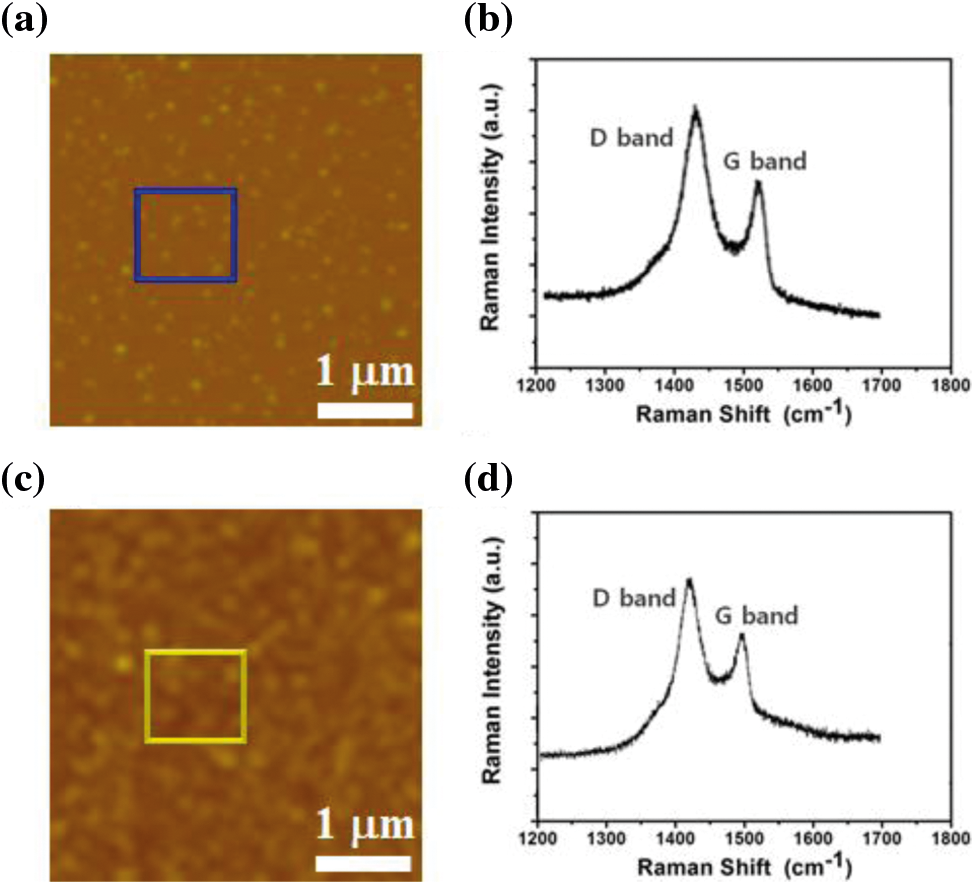
Figure 5: Characterization of chemical state in GQD layers in pristine, ON and OFF states. Raman intensity ratio maps of D and G bands in (a) ON state and (c) OFF state. (b) and (d) are Raman profiles of blue and yellow boxes in (a), (c)
Fig. 6a shows an HR-TEM image of the ON state after applying a negative bias to the upper electrode on the active layer. The non-uniform interface state was confirmed in the RGO-GQD/Au/graphene/ITO structure. Although the GQD region in RGO has a steadier and more densely stacked path than that of the off state, oxygen vacancies in the metal atomic layer increased at the interface, which means that defects in the interfacial region in RGO-GQD/Au/graphene increased. As shown in the TEM image, in the RGO-GQD and graphene layers, locally coupled atomic layer regions were located at the heterogeneous interface, and it can be judged that the RGO-GQD layers affected the charge transport path formation in the ON state, as shown in the red color box. An irregular interfacial region appeared in another localized area, and the boundary between the GQD conduction channel crystallization region and the RGO region could be identified.
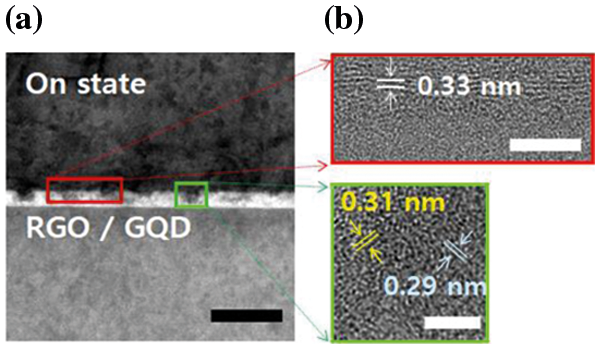
Figure 6: TEM image of RGO-GQD/Au layer. Scale bar indicates 20 nm. Inset of right panel: high-resolution TEM image showing GQDs. Scale bar, 5 nm
The composite RGO-GQD region has more regular and densely stacked GQDs than does the conventional GO thin film, which means that the crystallinity of the composite RGO-GQD region is increased. To avoid an abruptly formed conduction path, the effect of a barrier layer on the graphene/ITO interface was investigated. As can be seen in the HR-TEM images, the diameters of the GQDs at different locations in the RGO were uniformly distributed in the range of 3.6–7.5 nm, as shown in the green color box. In the ON state, it can be inferred that the GQD layer in the RGO is essential to forming a conductive charge transport layer. An irregular stack structure appeared in the localized region, and the boundary between the crystalline region and the randomly stacked region could be distinguished. Because typical thin GO layers have non-uniform thickness and roughness, creating a local electric field is not easy.
Figs. 7a and 7b is an HR-TEM image of the RGO-GQD/graphene/ITO layer in the ON and OFF states. The insets in the figures are HR-TEM images indicated in the red and blue rectangular regions of (c) and (d), respectively. The observation is that GQD is organized into an RGO layer as nanoparticles that uniformly incorporate the interface of graphene in the ON state. It can be inferred that the atomic crystallinity of the GQD layer within the RGO layer increased. In contrast, the GQDs are activated into the RGO layer as an aggregation that non-uniformly penetrates the ITO substrate interface in the OFF state. We investigated the variation in the nanostructure of the RGO-GQD layers by HR-TEM analysis. After applying a negative bias to the electrode, a crystalline RGO-GQD region was found, which is related to a conductive path. This decreased the number of hexagonal carbon-oxygen bonds in the RGO layer and caused a relative increase in the number of carbon-carbon orbital bonds in the GQD layer.
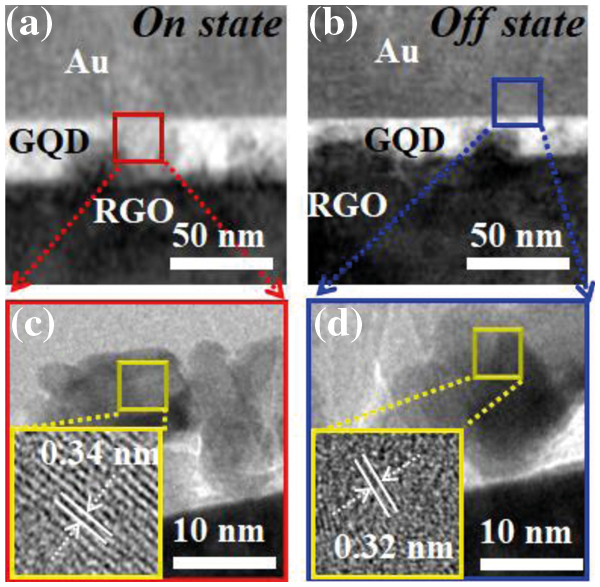
Figure 7: Cross-sectional TEM images of (a) conductive channel region in ON state and (b) OFF state; (c, d) corresponding cross-sectional HR-TEM images obtained in red and blue rectangular regions of (a, b), respectively
Furthermore, structural and chemical variation in the RGO-GQD layers can be proved by the d-spacing of the GQD clusters, as seen in the yellow box; these clusters have a considerable distance between them, caused by the desorption of RGO oxygen ions, as shown in Fig. 7c. However, the RGO layers in the yellow box are a relatively small distance apart due to the vast number of oxygen-functional groups without defects, as shown in Fig. 7d. The d-spacing results clearly prove the variation in RGO-GQD layers under an electric field. We found that conductive GQD pathways were created by movement of oxygen ions at interfaces in a strong electric field. The electric field is localized to a specific area of the GQDs because the thickness and roughness of the RGO layer are uniform, and the size and edge effects of the GQDs dominate.
During the ON state, oxygen and graphene layers play important roles in forming conductive graphene pathways. By applying a negative bias to the top electrode, the reproducibility characteristics of the resistive memory were confirmed to be related to the nanostructure. As the resistive properties were maintained during LRS, the nanostructures in the RGO-GQD devices appeared to be uniform, suggesting a correlation with the irreversible resistive switching behavioral properties. Observing the interface between the electrode and the low-dimensional structure reveals the presence of a very thin layer associated with defects. In the active layer heterostructure to which GQD is applied, surface recombination and diffusion of Au ions occur due to rapid energy transfer at the interface. The GQD composite layer resolves the energy band mismatch between this heterostructure and the grains generated from the heterogeneous interface structure. Therefore, carrier movement occurs without clogging from Au adatom to GQD when the graphene layer is applied to the RGO active layer. This confirms the possibility of effective filament channels for charge recombination and transport in RGO-based resistive memories.
Fig. 8a shows the DC switching results measured over 30 loops, used to analyze the resistive memory characteristics of the flexible RGO-GQD structure. As can be seen in the figure, the butterfly shape during DC switching hardly changed after cycling, indicating that the designed RGO-GQD structure-based device did not degrade during the fabrication process. The synaptic crossbar array device was set up with a single 15 ns wide pulse (2.3 V high), and the active stay resistance was reduced by a factor of 10 during DC switching. These electrical properties allowed the RGO-GQD structure-based devices to exist in a RESET range of <10 ns per bit for multi-bit implementation of the synaptic crossbar. The LRS and HRS show uniform distributions, and the HRS shows a slightly wider distribution than LRS at the selected bias.
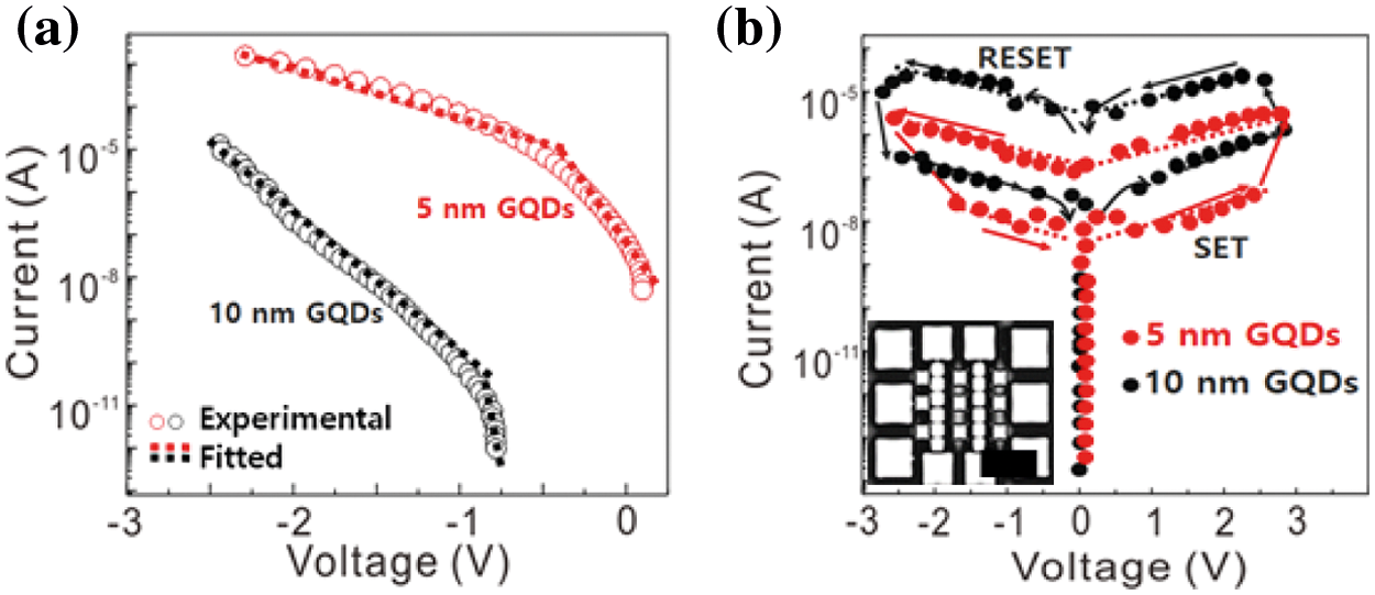
Figure 8: (a) I–V curves of Au/RGO-GQDs/Au/graphene/ITO/PI memory devices plotted on semi-logarithmic scale. (b) I–V curves of Au/RGO-GQDs/Au/graphene/ITO/PI memory devices plotted on semi-logarithmic scale. The inset is an optical microscopy image of RRAM crossbar device (scale bar: 200 μm)
The strong electric field across the electrode and the RGO-GQD layer at a positive bias voltage induced the oxygen ions in the negatively charged RGO to drift towards the top electrode interface. As a result, the height of the Schottky barrier between the electrode and the heterostructure interface decreased, and carrier diffusion through the tunneling barrier increased due to the reduction of defects in the RGO-GQD layer. This mechanism provides advantages compared to crossbar synapse devices. Through the electric field, the conductive RGO-GQD layer enabled uniform resistive memory value control through the structural transport of ions and the switch characteristics observed in flexible RRAM devices with well-defined interfacial defects and GQDs.
Fig. 8b shows the SET/RESET I–V curves of 15 devices, in which ten have 5 nm size GQDs and the rest have 10 nm size GQDs. The dramatic change of the ON/OFF state current was confirmed by looking at the RGO switching layer applied with 10 nm particle size and comparing it to the RGO-GQD layer coated to 5 nm particle size. For the SET/RESET voltages, it was observed that the electrical properties of the RGO active layer RRAM synaptic crossbar to which GQDs were applied by size increased to 2.4/3.3 V for SET/RESET. The ON/OFF current ratio is reduced to 103 of that of the discrete RRAM crossbar with GQDs. This is because the mobile ions penetrating the RGO-GQDs conductive path were transferred to the active area by the depression of the voltage, which had an amplitude of 2.9 V. Here, the various pulse frequencies and pulse widths were changed at 10 Hz and 20 ms, respectively. The thickness of the RGO-GQDs layer was set in a range of 10–25 nm by varying the concentration of GQDs, whereas the active region was fixed at 25 × 25 μm2. A compliance current of 5 mA was applied to protect the device. The initial switching occurred at Vf = 2.31 V for 1.5 wt% GQSs, and Vf changed from 2.12 to 2.85 V when increasing from 1.0 to 2.5 wt% of the GQDs. When the sweep voltage was changed to 5 V, there was no resistive switching characteristic at 5.0 wt% of GQDs. In the next switching stage, at 1.5 wt% of GQDs, the HRS was maintained when bias was applied below 1.2 V, when bias was applied at over 2.84 V, the current rapidly increased. As a result, the SET/RESET I–V loops characteristic curve under a depression pulse of 2.5 V exhibited the best symmetricity. Therefore, we optimized the SET/RESET I–V characteristics of the designed synapse array device by adjusting the carrier penetration behavior through variation of the active path thickness and region of the crossbar interface.
Fig. 9a shows the electrical characteristics measured under various temperature conditions in the range of 150∼300 K. The High Resistance State (HRS) and Low Resistance State (LRS) show the change in resistance. The carriers penetrated the composite RGO-GQD layers under an electric field, and conductive metal filaments composed of GQD ions were produced. As the temperature increases, the resistance decreases in the HRS and LRS, and the conduction path of the composite RGO-GQDs improves. According to the temperature, the presence of GQDs, and the composite RGO high resistance stemming from linked oxygen functional groups that can be dissociated, the resistance change in the state is more significant than the resistance in the LRS. Based on these experimental results, the high-temperature region was found to be consistent with the Arrhenius model. Defects of the interface in the RGO-GQDs, and the ejected carriers, support the electrical conduction of the composite RGO structure. Furthermore, the flexible RGO-GQD device showed that SET/RESET cycling endurance could be greater than 200. To predict how fast the RRAM device can operate, SET and RESET operations were performed with uniform pulses with width ranging from 20 μs to 15 ns, which is the resolution of the pulse generator. LRS is caused by ion diffusion in the top electrode. It can be inferred that, related to the composite RGO region with metallic behavior, the formation of a conductive path (CP) occurs.
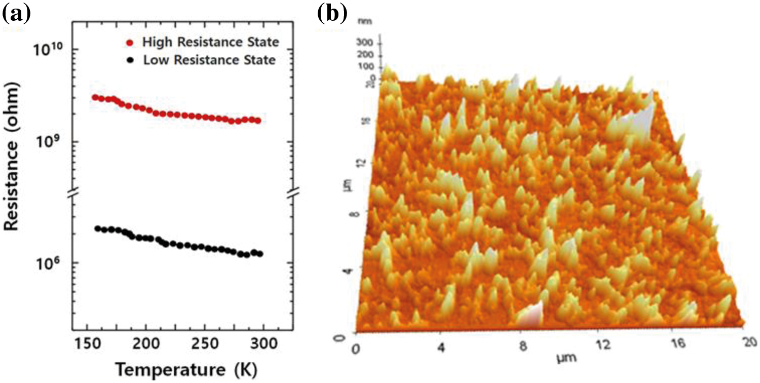
Figure 9: (a) Temperature dependence of resistance at HRS and LRS. (b) Conductive AFM images of RGO-GQDs/Au/graphene/ITO/PI at LRS and HRS after removing Au top electrode; scale bar indicates 0.3 μm
The structure of the CP was analyzed using conductive AFM, with results shown in Fig. 9b. After removing the top Au electrode at a voltage of 0.5 V, conductivity of state in the measured HRS and LRS. The AFM image shows a relatively high current, indicating that a negative bias is applied to the upper electrode. It can be seen that a local conduction path is formed. For CMOS device implementation, because process flexibility of the array design is required, a system of resistive memory crossbars can incorporate electrically characterized memristors. We aimed to develop a monolithically integrated array capable of obtaining stable resistive memory performance in RGO-GQD flexible devices.
To improve performance and portability, and to reduce size, electronic devices are evolving to become more flexible, such as including low-power devices, batteries, and sensors to improve performance and portability and reduce size. Flexible electronics bend when, as rolling and torsion occur, as such, mechanical reliability during cyclic deformation is an important characteristic. We investigated the bending stress of RGO-GQDs layers on flexible polyimide substrates with different thicknesses using single-layer and bi-layer bending models and monitored the electrical resistance of the devices with an RGO-GQDs during a bending fatigue test. Fig. 10a shows the variation of the crossbar synapse array with an RGO-GQDs by under repeated bending of up to 500 times iterations for R = 5 mm. Even after the bending test, more than 95% of the resistive switching value is was maintained.
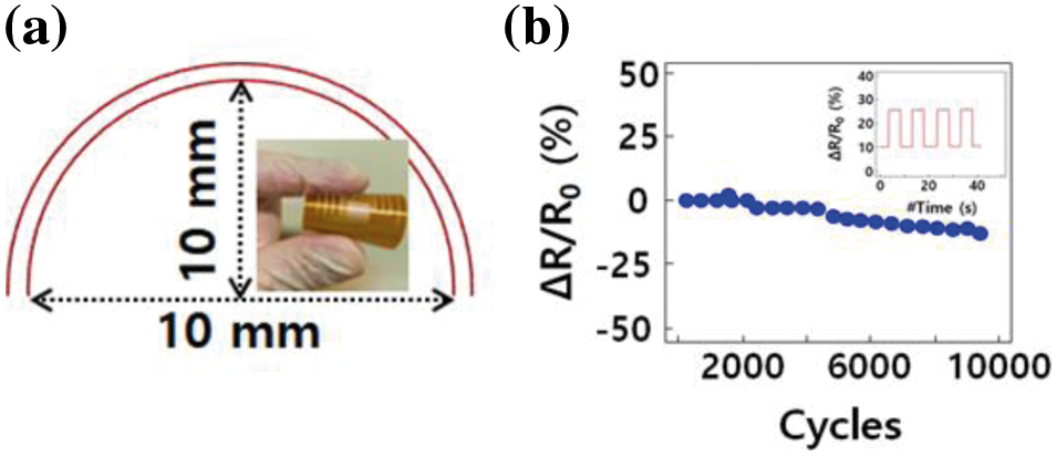
Figure 10: (a) Schematic representation and the insets describing the bending tests, and show a real image of a typical memristive sample. (b) Changes of normalized ΔR/R0 (%) as functions of bending cycles at R = 5 mm for devices under outer bending
To clarify the cause of the device degradation, we also confirmed the evolution of normalized ΔR/R0 (%) changes as functions of bending cycles in the same way. After 100 cycles, the relative ΔR/R0 (%) increased by 6%, as shown in Fig. 10b, which the cracking of the interface can interpret shows this effect. Therefore, an exact design of the to determine applied mechanical strain applied during bending is necessary to model highly reliable flexible electronics. These results suggest that the defect-free RGO-GQDs are very promising as a flexible memristive devices. Compared to these devices, our synapse array with a GQDs showed a low cycle-to-cycle variation of less than 3% and a high recognition rate of 95.5%. From the perspective, in terms of cycle-to-cycle variation, we can say that the proposed device is acceptable for implementing an artificial neural network.
This work successfully implemented a reproducible flexible crossbar synaptic array based on a low-dimensional structure with GQD-RGO layers. This two-dimensional synapse array was achieved by adopting a crossbar synapse with a GQD structure. The mobile carriers in the RGO penetrated the interface of a CF channel located at the crossbar between the top and bottom electrode, which resulted in resistive memory structures with excellent conductance due to GQD ion pathways. The crossbar synaptic device showed reliable long-term plastic behavior because predictable currents did not return to their initial values. Raman spectrum analysis indicate a D-band of 1421 cm−1 that occurs due to disorder, expressed as an atomic characteristic of carbon in the sp2 hybridized structure, and a G-band of 1518 cm−1 that corresponds to the graphite structure. The intensity ratio I(D)/I(G) of the D peak to the G peak is about 0.96, and is related to the size and edge structure of the GQDs coated on the RGO. In the ON state, it can be inferred that the GQD layer in the RGO is an essential variable in forming a conductive charge transport layer. We found that conductive GQD pathways were created by the movement of oxygen ions at the interface in a strong electric field. The electric field is localized to a specific area of the GQD because the thickness and roughness of the RGO layer are uniform, and the size and edge effects of the GQDs dominate. These results will impact emerging VLSI design and lead to the optimization of ANNs.
Funding Statement: The authors received no specific funding for this study.
Conflicts of Interest: The authors declare that they have no conflicts of interest to report regarding the present study.
1. N. Takeki, W. Zhigiang, M. Shusaku, Y. Ryutaro and T. Takeshi, “Conductive flament scaling of TaOx bipolar ReRAM for improving data retention under low operation current,” IEEE (Institute of Electrical and Electronics Engineers) Transactions on Electron Devices, vol. 60, no. 4, pp. 1384–1389, 2013. [Google Scholar]
2. J. Perelaer, P. J. Smith, D. Mager, D. Soltman and U. S. Schubert, “Printed electronics: The challenges involved in printing devices, interconnects, and contacts based on inorganic materials,” Journal of Materials Chemistry, vol. 20, no. 39, pp. 8446–8453, 2010. [Google Scholar]
3. T. Li, W. Xu, L. Wang, Y. Ren and J. Xia, “An integrated artificial neural network-based precipitation revision model,” KSII (Korean Society for Internet Information) Transactions on Internet and Information Systems, vol. 15, no. 5, pp. 1690–1707, 2021. [Google Scholar]
4. K. Kim and J. Lee, “Deep CNN based pilot allocation scheme in massive MIMO systems,” KSII (Korean Society for Internet Information) Transactions on Internet and Information Systems, vol. 14, no. 10, pp. 4214–4230, 2020. [Google Scholar]
5. S. V. Prasanna, K. Balasubadra, K. Saravanan, V. S. Arjun and S. Malarkodi, “Multi label deep learning classification approach for false data injection attacks in smart grid,” KSII (Korean Society for Internet Information) Transactions on Internet and Information Systems, vol. 15, no. 6, pp. 2168–2187, 2021. [Google Scholar]
6. S. Ali, J. Bae and C. H. Lee, “Printed non-volatile resistive switches based on zinc stannate (ZnSnO3),” Current Applied Physics, vol. 16, no. 7, pp. 757–762, 2016. [Google Scholar]
7. S. Ali, J. Bae, C. H. Lee, K. H. Choi and Y. H. Doh, “All-printed and highly stable organic resistive switching device based on graphene quantum dots and polyvinylpyrrolidone composite,” Organic Electronics, vol. 25, pp. 225–231, 2015. [Google Scholar]
8. M. J. Catenacci, P. F. Flowers, C. Cao, J. B. Andrews and B. J. Wiley, “Fully printed memristors from Cu-SiO2 core-shell nanowire composites,” Journal of Electronic Materials, vol. 46, pp. 4596–4603, 2017. [Google Scholar]
9. A. Mahajan, C. D. Frisbie and L. F. Francis, “Optimization of aerosol jet printing for high-resolution, high-aspect ratio silver lines,” ACS (American Chemical Society) Applied Materials & Interfaces, vol. 5, no. 11, pp. 4856–4864, 2013. [Google Scholar]
10. E. Jabari and E. Toyserkani, “Micro-scale aerosol-jet printing of graphene interconnects,” Carbon, vol. 91, pp. 321–329, 2015. [Google Scholar]
11. E. Jabari and E. Toyserkani, “Aerosol-jet printing of highly flexible and conductive graphene/silver patterns,” Materials Letters, vol. 174, pp. 40–43, 2016. [Google Scholar]
12. S. Kim, S. W. Hwang, M. -K. Kim, S. -H. Choi and B. H. Hong, “Anomalous behaviors of visible luminescence from graphene quantum dots: Interplay between size and shape,” ACS (American Chemical Society) Nano, vol. 6, no. 9, pp. 8203–8208, 2012. [Google Scholar]
13. C. W. P. Shi, X. Shan, G. Tarapata, R. Jachowicz and H. T. Hui, “Fabrication of wireless sensors on flexible film using screen printing and via filling,” Microsystem Technologies, vol. 17, no. 4, pp. 661–667, 2011. [Google Scholar]
14. W. -Y. Chang, T. -H. Fang, H. -J. Lin, Y. -T. Shen and Y. -C. Lin, “A large area flexible array sensors using screen printing technology,” Journal of Display Technology, vol. 5, no. 6, pp. 178–183, 2009. [Google Scholar]
15. H. Kempa, M. Hambsch, K. Reuter, M. Stanel and A. C. Hubler, “Complementary ring oscillator exclusively prepared by means of gravure and flexographic printing,” IEEE (Institute of Electrical and Electronics Engineers) Transactions on Electron Devices, vol. 58, no. 8, pp. 2765–2769, 2011. [Google Scholar]
16. P. F. Moonen, I. Yakimets and J. Huskens, “Fabrication of transistors on flexible substrates: From mass-printing to high-resolution alternative lithography strategies,” Advanced Materials, vol. 24, no. 41, pp. 5526–5541, 2012. [Google Scholar]
17. D. B. Hall, P. Underhill and J. M. Torkelson, “Spin coating of thin and ultrathin polymer films,” Polymer Engineering and Science, vol. 38, no. 12, pp. 2039–2045, 1998. [Google Scholar]
18. K. Yan, M. Peng, X. Yu, X. Cai and D. Zou, “High-performance perovskite memristor based on methyl ammonium lead halides,” Journal of Materials Chemistry C, vol. 4, no. 7, pp. 1375–1381, 2016. [Google Scholar]
19. M. Nelo, M. Sloma, J. Kelloniemi, J. Puustinen and H. Jantunen, “Inkjet-printed memristor: Printing process development,” Japanese Journal of Applied Physics, vol. 52, no. 5, pp. 1–10, 2013. [Google Scholar]
20. K. Rajan, S. Bocchini, A. Chiappone, I. Roppolo and A. Chiolerio, “Spin-coated silver nanocomposite resistive switching devices,” Microelectronic Engineering, vol. 168, pp. 27–31, 2017. [Google Scholar]
21. C. -F. Lin, B. -K. Wang, C. Tiu and T. -J. Liu, “On the pinning of downstream meniscus for slot die coating,” Advances in Polymer Technology, vol. 32, no. S1, pp. E249–E257, 2013. [Google Scholar]
22. L. Hu, H. S. Kim, J. -Y. Lee, P. Peumans and Y. Cui, “Scalable coating and properties of transparent, flexible, silver nanowire electrodes,” ACS (American Chemical Society) Nano, vol. 4, no. 5, pp. 2955–2963, 2010. [Google Scholar]
23. J. Simmons and R. Verderber, “New thin-film resistive memory,” Radio and Electronic Engineer, vol. 34, no. 2, pp. 81–89, 1967. [Google Scholar]
24. E. L. Cook, “Model for the resistive-conductive transition in reversible resistance-switching solids,” Journal of Applied Physics, vol. 41, no. 2, pp. 551–554, 1970. [Google Scholar]
25. T. -M. Lee, S. -H. Lee, J. -H. Noh, D. -S. Kim and S. Chun, “The effect of shear force on ink transfer in gravure offset printing,” Journal of Micromechanics and Microengineering, vol. 20, no. 125026, pp. 1–8, 2010. [Google Scholar]
26. N. Choi, H. Wee, S. Nam, J. Lavelle and M. Hatalis, “A modified offset roll printing for thin film transistor applications,” Microelectronic Engineering, vol. 91, pp. 93–97, 2012. [Google Scholar]
27. T. -M. Lee, J. -H. Noh, I. Kim, D. -S. Kim and S. Chun, “Reliability of gravure offset printing under various printing conditions,” Journal of Applied Physics, vol. 108, no. 102802, pp. 1–6, 2010. [Google Scholar]
28. D. Sung, A. de la Fuente Vornbrock and V. Subramanian, “Scaling and optimization of gravure-printed silver nanoparticle lines for printed electronics,” IEEE (Institute of Electrical and Electronics Engineers) Transactions on Components and Packaging Technologies, vol. 33, no. 1, pp. 105–114, 2010. [Google Scholar]
29. J. Noh, K. Jung, J. Kim, S. Kim and G. Cho, “Fully gravure printed flexible full adder using SWNT-based TFTs,” IEEE (Institute of Electrical and Electronics Engineers) Electron Device Letters, vol. 33, no. 11, pp. 1574–1576, 2012. [Google Scholar]
30. H. Park, H. Kang, Y. Lee and G. Cho, “Fully roll-to-roll gravure printed rectenna on plastic foils for wireless power transmission at 13.56 MHz,” Nanotechnology, vol. 23, no. 34, pp. 1–5, 2012. [Google Scholar]
31. A. Perl, D. N. Reinhoudt and J. Huskens, “Microcontact printing: Limitations and achievements,” Advanced Materials, vol. 21, no. 22, pp. 2257–2268, 2009. [Google Scholar]
32. T. Kaufmann and B. J. Ravoo, “Stamps, inks and substrates: Polymers in microcontact printing,” Polymer Chemistry, vol. 1, no. 4, pp. 371–387, 2010. [Google Scholar]
33. B. Li, J. Zhang and H. Ge, “A sandwiched flexible polymer mold for control of particle-induced defects in nanoimprint lithography,” Applied Physics A, vol. 110, no. 1, pp. 123–128, 2013. [Google Scholar]
34. S. A. Ruiz and C. S. Chen, “Microcontact printing: A tool to pattern,” Soft Matter, vol. 3, no. 2, pp. 168–177, 2007. [Google Scholar]
35. Y. Sun and J. A. Rogers, “Inorganic semiconductors for flexible electronics,” Advanced Materials, vol. 19, no. 15, pp. 1897–1916, 2007. [Google Scholar]
36. R. S. Dahiya, A. Adami, C. Collini and L. Lorenzelli, “Fabrication of single crystal silicon micro-/nanostructures and transferring them to flexible substrates,” Microelectronic Engineering, vol. 98, pp. 502–507, 2012. [Google Scholar]
37. A. J. Baca, J. -H. Ahn, Y. Sun, M. A. Meitl and J. A. Rogers, “ChemInform abstract: Semiconductor wires and ribbons for high-performance flexible electronics,” ChemInform, vol. 39, no. 43, pp. 5524–5542, 2008. [Google Scholar]
38. L. Chua, “Memristor—The missing circuit element,” IEEE (Institute of Electrical and Electronics Engineers) Transactions Circuit Theory, vol. CT-18, no. 5, pp. 507–519, 1971. [Google Scholar]
39. D. B. Strukov, G. S. Snider, D. R. Stewart and R. S. Williams, “The missing memristor found,” Nature, vol. 453, no. 7191, pp. 80, 2008. [Google Scholar]
40. N. K. Upadhyay, W. Sun, P. Lin, S. Joshi and R. Midya et al., “A memristor with low switching current and voltage for 1s1r integration and array operation,” Advanced Electronic Materials, vol. 6, no. 1901411, pp. 1–10, 2020. [Google Scholar]
41. G. S. Kim, H. Song, Y. K. Lee, J. H. Kim and C. S. Hwang, “Defect-engineered electroforming-free analog HfOx memristor and its application to the neural network,” ACS (American Chemical Society) Advanced Materials Interfaces, vol. 11, pp. 47063–47072, 2019. [Google Scholar]
42. J. P. Strachan, J. J. Yang, L. A. Montoro, C. A. Ospina and R. S. Williams, “Characterization of electroforming-free titanium dioxide memristors,” Beilstein Journal of Nanotechnology, vol. 4, pp. 467–473, 2013. [Google Scholar]
43. T. D. Dongale, K. P. Patil, S. B. Mullani, K. V. More and R. K. Kamat, “Investigation of process parameter variation in the memristor based resistive random access memory (RRAMEffect of device size variations,” Materials Science in Semiconductor Processing, vol. 35, pp. 174–180, 2015. [Google Scholar]
44. S. Kim, S. Jung, M. H. Kim, Y. -C. Chen and B. G. Park, “Scaling effect on silicon nitride memristor with highly doped Si substrate,” Small, vol. 14, no. 1704062, pp. 1–8, 2018. [Google Scholar]
 | This work is licensed under a Creative Commons Attribution 4.0 International License, which permits unrestricted use, distribution, and reproduction in any medium, provided the original work is properly cited. |