DOI:10.32604/cmc.2022.027404
| Computers, Materials & Continua DOI:10.32604/cmc.2022.027404 | |
| Article |
A 78-MHz BW Continuous-Time Sigma-Delta ADC with Programmable VCO Quantizer
1Institute of RF- & OE-ICs, Southeast University, Nanjing, 210096, China
2Jiangsu Key Construction Laboratory of IoT Application Technology, Wuxi Taihu University, Wuxi, 214064, China
3Polytechnic University of Madrid, Madrid, 28031, Spain
*Corresponding Author: Qiao Meng. Email: mengqiao@seu.edu.cn
Received: 17 January 2022; Accepted: 04 March 2022
Abstract: This article presents a high speed third-order continuous-time (CT) sigma-delta analog-to-digital converter (SDADC) based on voltage-controlled oscillator (VCO), featuring a digital programmable quantizer structure. To improve the overall performance, not only oversampling technique but also noise-shaping enhancing technique is used to suppress in-band noise. Due to the intrinsic first-order noise-shaping of the VCO quantizer, the proposed third-order SDADC can realize forth-order noise-shaping ideally. As a bright advantage, the proposed programmable VCO quantizer is digital-friendly, which can simplify the design process and improve anti-interference capability of the circuit. A 4-bit programmable VCO quantizer clocked at 2.5 GHz, which is proposed in a 40 nm complementary metal-oxide semiconductor (CMOS) technology, consists of an analog VCO circuit and a digital programmable quantizer, achieving 50.7 dB signal-to-noise ratio (SNR) and 26.9 dB signal-to-noise-and-distortion ration (SNDR) for a 19 MHz − 3.5 dBFS input signal in 78 MHz bandwidth (BW). The digital quantizer, which is programmed in the Verilog hardware description language (HDL), consists of two-stage D-flip-flop (DFF) based registers, XOR gates and an adder. The presented SDADC adopts the cascade of integrators with feed-forward summation (CIFF) structure with a third-order loop filter, operating at 2.5 GHz and showing behavioral simulation performance of 92.9 dB SNR over 78 MHz bandwidth.
Keywords: Sigma-delta ADC; oversampling converter; VCO; noise-shaping; programmable quantizer
The analog-to-digital converter (ADC), as an interface circuit connecting physical signals and digital signals that can process information, is of great importance to promote information technology. In particular, with the rapid development of artificial intelligence [1], the Internet of Things [2], cloud computing and 6 G communication technologies [3], high-bandwidth and low-power ADC has become a research hotspot [4,5]. Sigma-delta ADC is widely recognized for its unique oversampling and noise-shaping techniques, achieving lower cost and higher performance. The sigma-delta architecture consists of more digital circuits, which is more conducive to integration with digital systems and meets the requirements of CMOS technology. Compared with discrete-time sigma-delta ADC, continuous-time sigma-delta ADC (CT-SDADC) has an implicit anti-aliasing filter [6], which reduces power consumption and increases signal bandwidth to 100 MHz [7]. In order to further improve the performance of SDADC, the order of sigma-delta modulator or the number of quantizer bit is usually increased, but this inevitably leads to complex structure, high energy consumption and stability issues.
Due to the technology scaling, the operating voltage is getting lower and lower, which challenges the design of traditional analog voltage-based ADC [8] but benefits the time-based digital circuits [9,10]. As a voltage-to-frequency converter, VCO quantizer (VCOQ) can realize phase-based quantization, avoid the restriction of reduced power supply voltage [11], and becomes one of the representatives of time-based quantizer [12–14].
CT-SDADC based on VCOQ becomes popular, which not only simplifies the structure of sigma-delta ADC but also shows excellent performance. VCOQ has the desirable properties of multi-bit quantization, high sampling frequency and intrinsic first-order noise-shaping [15], which suppress in-band noise and further improve resolution [16]. As an added advantage, dynamic element matching (DEM) can be automatically realized to reduce the nonlinearity introduced by digital-to-analog converter (DAC) element mismatch [17]. Moreover, as the VCO output is a binary signal, it can be directly integrated with the digital circuit to facilitate the subsequent digital calibration and digital filtering [18]. SDADC usually adopts ring voltage-controlled oscillator (RVCO), which makes use of negative feedback of gate delays to generate oscillation. Generally, RVCO is composed of an odd number of inverters connected end to end. Each inverter outputs periodic signals of the same frequency but with different phases, that is, the phases can be quantized to represent the input voltage [19].
However, the conventional VCOQ-SDADCs mentioned above are always composed of operational transconductance amplifiers, which brings difficulties to design circuits. In this paper, the digital programmable technique is used to simplify the design process and enhance performance. The analog VCO is designed in 40 nm CMOS technology, and the digital programmable quantizer is implemented using Verilog HDL. The proposed programmable VCOQ-SDADC (PVCOQ-SDADC) provides a compact design with high speed by using digital programmable structure instead of analog blocks of conventional architectures.
The rest of this article is organized as follows. In Section 2, the proposed PVCOQ-SDADC architecture is introduced. Section 3 presents a 4-bit programmable VCOQ (PVCOQ) circuit details. Section 4 describes the PVCOQ-SDADC model details and shows behavioral simulation results, while Section 5 includes concluding remarks for this article.
The proposed PVCOQ-SDADC adopts one-stage third-order structure based on PVCOQ instead of the conventional flash quantizer, as shown in Fig. 1. For this analysis, SDADC is considered to be discrete-time and represented by the loop transfer function L(z), the signal transfer function (STF) and the noise transfer function (NTF). The input analog signal Vin passes through the loop filter L(z) and becomes the signal
where Avcoq is the quantizer gain. The NTF of the third-order SDADC is
showing that the NTF of PVCOQ-SDADC is
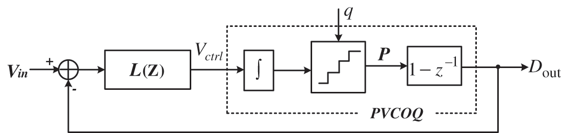
Figure 1: Block diagram of the proposed PVCOQ-SDADC
The proposed PVCOQ consists of an analog VCO and a digital programmable quantizer, shown in Fig. 2. The analog VCO is implemented with transistor-level circuits in 40 nm CMOS technology, including delay cells and buffers. The digital quantizer, which is programmed in Verilog HDL, consists of two-stage DFF based registers, XOR gates and an adder. The output of each delay cell is buffered and then sampled by the clock Clk_s, transferred to discrete phase signals P[k] and P[k−1]. Through XOR gates, the difference of the phase signals is obtained, and the absolute value is added to get the quantized number Dout.
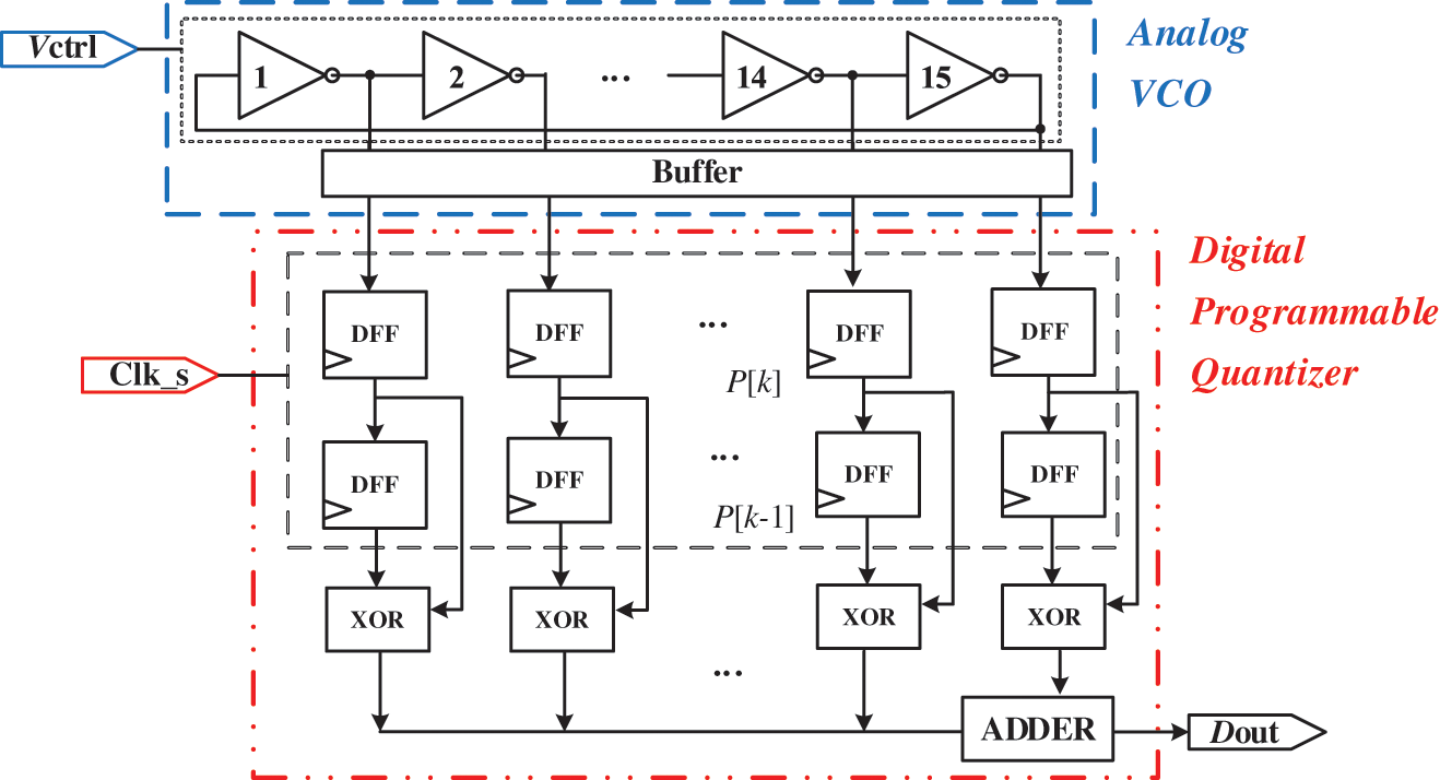
Figure 2: Block diagram of the proposed PVCOQ
A 4-bit PVCOQ model is built in Simulink, requiring 15-delay stage VCO with the input signal
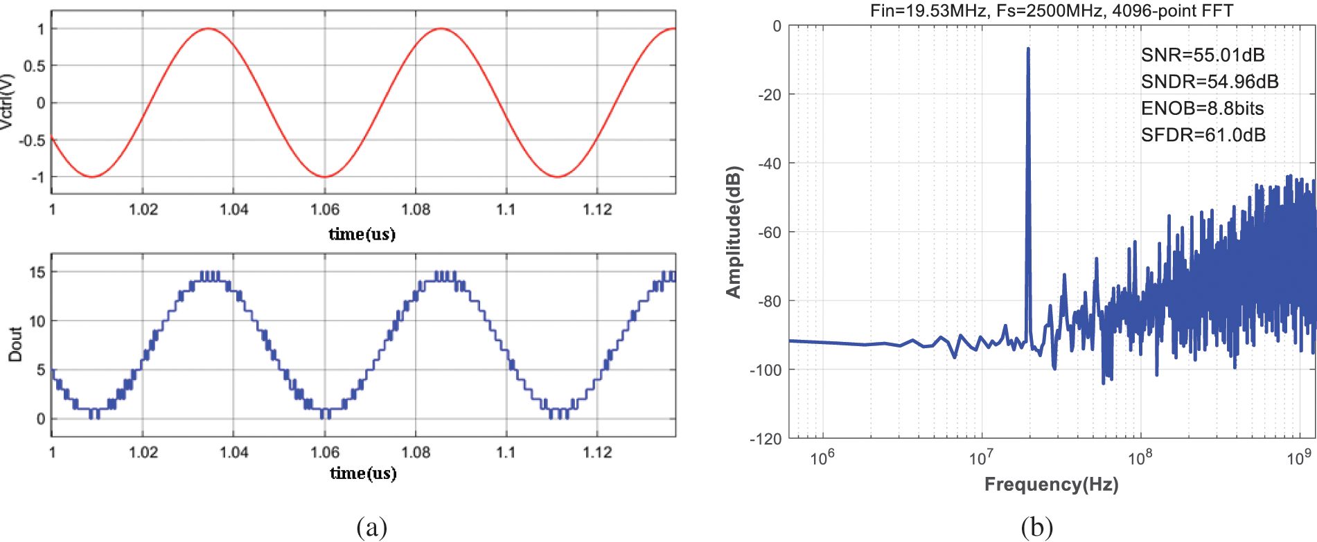
Figure 3: Simulated waveforms (a) and PSD (b) for the ideal open-loop PVCOQ
The proposed analog VCO circuit consists of 15-delay stage ring oscillator and buffers, shown in Fig. 4. The input voltage
where td is the gate delay time,
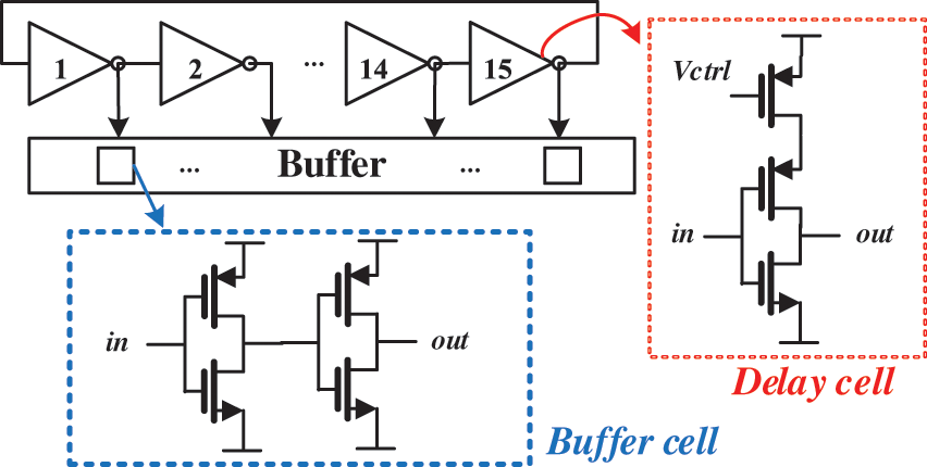
Figure 4: Schematic of the proposed analog VCO
The tuning characteristic is simulated at 27 °C and TT process angle, showing the frequency range from 1.285 GHz to 140 MHz in Fig. 5. This structure supports a high clock rate since the minimum delay is only around 26 ps. The average slope of the tuning curve is the oscillation gain Kvco.
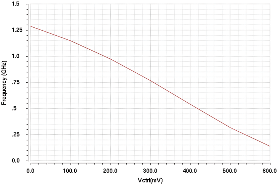
Figure 5: Tuning characteristic of the proposed VCO
As the tuning curve is not an ideal straight line, polynomial fitting is performed and the curve can be represented by
According to the nonlinearity formula [20]
where fFS is the full-scale frequency, Δfmax is the maximum frequency difference between the ideal line and the actual tuning curve, and N is the number of bits in the quantizer. The nonlinearity of the proposed VCO is 0.0381, less than
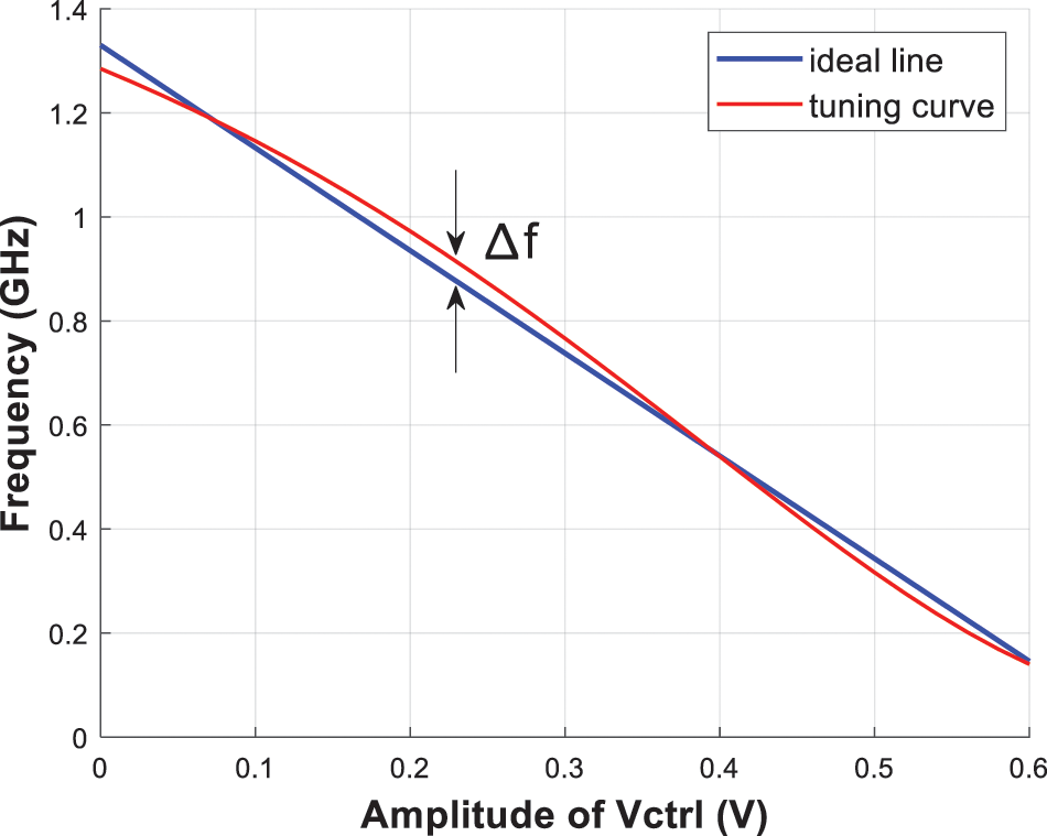
Figure 6: Tuning curve of the proposed VCO compared with the ideal line
3.2 Digital Programmable Quantizer
The essence of time-based VCOQ is to accumulate the number of delay cells flipped during one sample period Ts. The greater the gate delay time, the fewer delay cells can flip in a sample period, and the smaller the quantizer output. The ideal output of the 4-bit quantizer is
According to Eqs. (3) and (5), there is a defined relationship between the delay time td and the input voltage
The digital quantizer is programmed in Verilog HDL, saving much design time and showing good portability compared with analog circuits. The outputs of the proposed digital programmable quantizer under various conditions are shown in Fig. 7, where p[14:0] represents the output of 15 delay cells in VCO, and XOR_out [14:0] is the result after differential and absolute value operations. As the input voltage
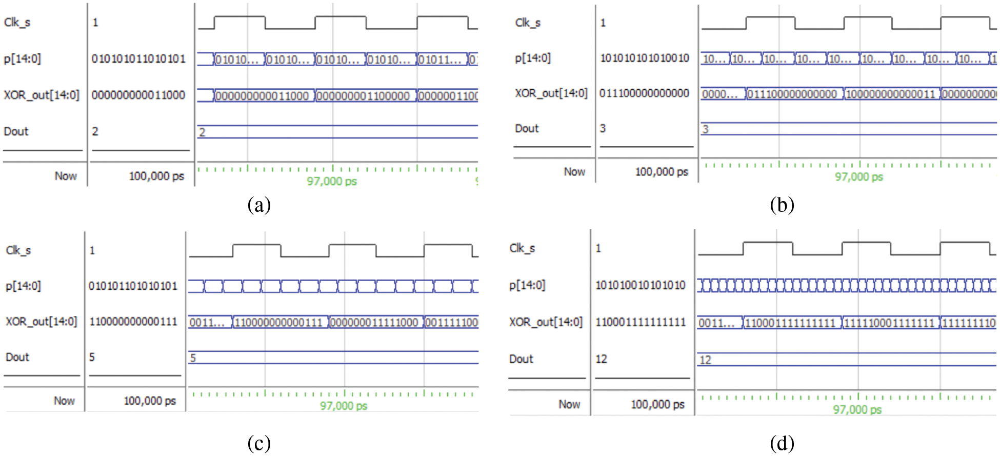
Figure 7: Simulation waveforms of the programmable quantizer at sampling frequency 1.7 GHz when (a) td = 300 ps, (b) td = 200 ps, (c) td = 120 ps, (d) td = 50 ps
Tab. 1 lists the output data of the digital quantizer in any five consecutive sampling periods shown in Fig. 8, where Clk represents the number of sampling periods. Between adjacent samples, VCO always oscillates from the unstable inverter corresponding to the red italic in Tab. 1, and the number of inverters flipped in each sampling period is the digital output. As shown in Tab. 1, take the first sampling Clk = 1 for example, the oscillation starts from the unstable inverter P[10] in the zeroth sample, and 11 inverters followed from P[11] to P[6] are flipped consecutively, resulting in the output Dout = 12. In the same way, when Clk = 3, the oscillation starts from the unstable inverter P[4] in the 2nd sample, and 11 inverters followed are flipped, with the same output Dout = 12. Therefore, regardless of which inverter starts the flip, the quantizer output Dout is determined only by the delay time td at the same sampling frequency, that is, controlled only by the input voltage.
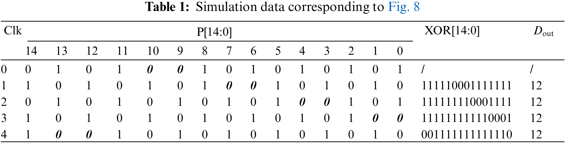
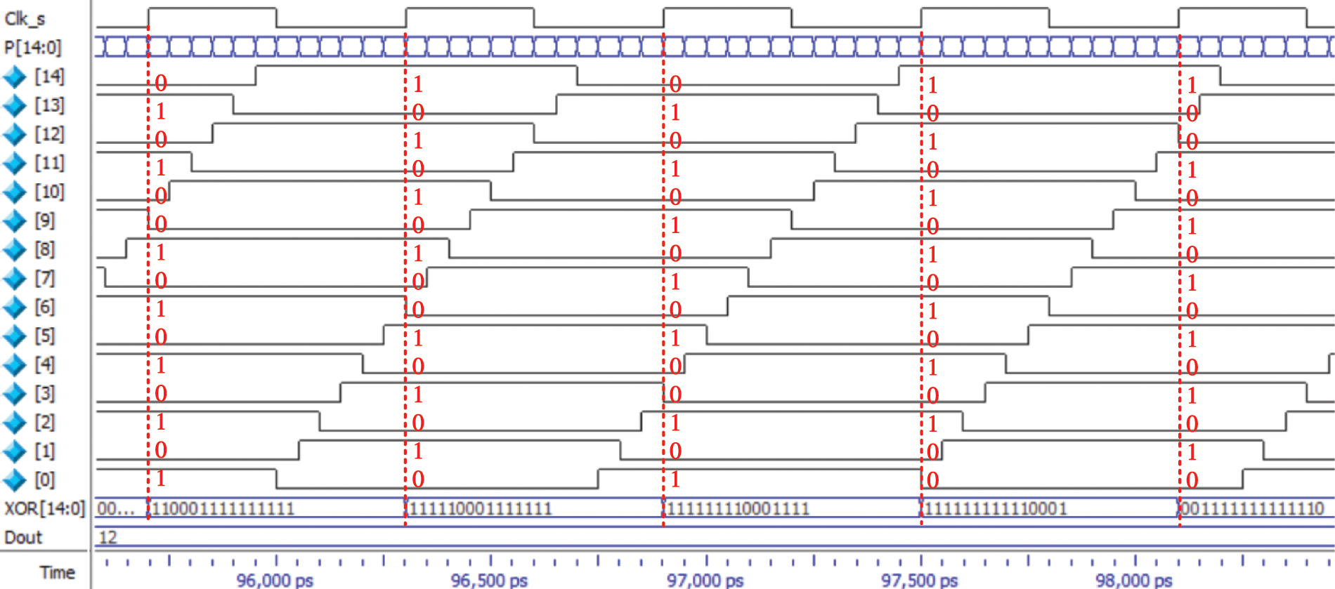
Figure 8: Simulation waveform details of the programmable quantizer when Fs = 1.7 GHz and td = 50 ps
The transient simulation of the proposed PVCOQ is implemented in AMS, with 2.5 GHz sampling frequency in 40 nm CMOS technology. The simulation results for a full-scale input signal are shown in Fig. 9. As the output frequency of the proposed VCO is inversely proportional to the input voltage, the phase between the output Dout and the input
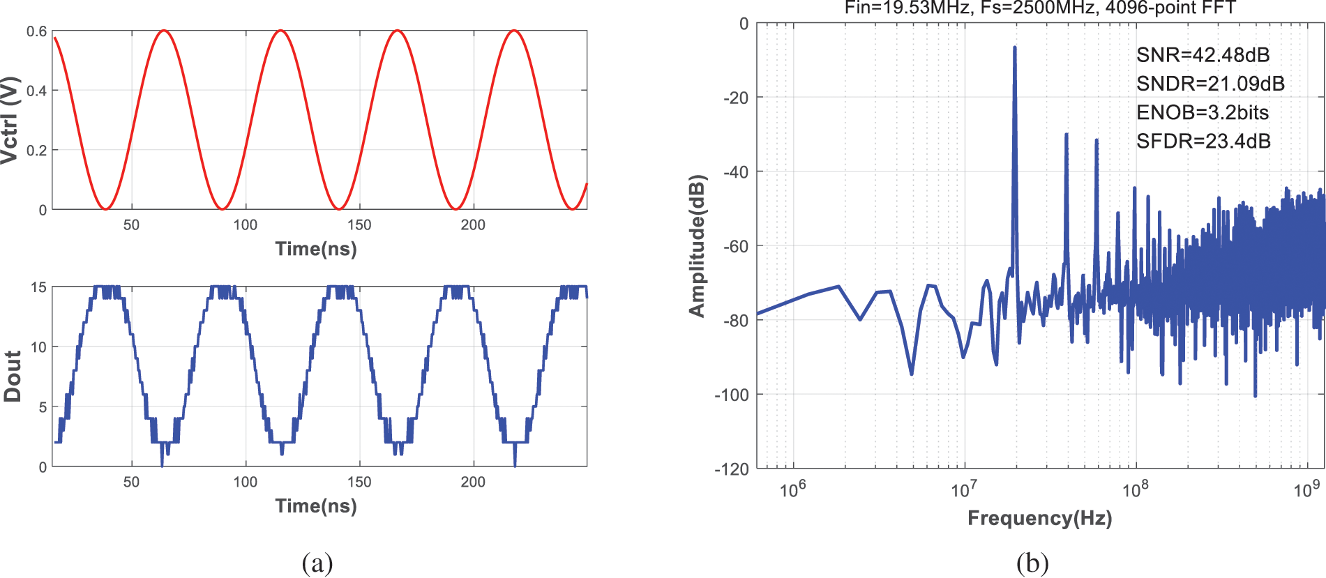
Figure 9: Simulated waveforms (a) and PSD (b) of the proposed PVCOQ for a 19 MHz full-scale input signal
When the input swing reduced to −3.5 dBFS, the waveforms and spectrum diagram of the PVCOQ are shown in Fig. 10. The proposed PVCOQ has a peak SNR/SNDR of 50.7 dB/26.9 dB and a 27.4 dB SFDR for a 78 MHz signal bandwidth. Fig. 11 exhibits the power spectral density for −9.5 dBFS and −15.6 dBFS input signal, achieving 31.8 and 34.9 dB SNDR respectively. It can be seen that, when the output swing requirements are not very strict, the negative effect of VCO nonlinearity can be mitigated by decreasing the input amplitude.
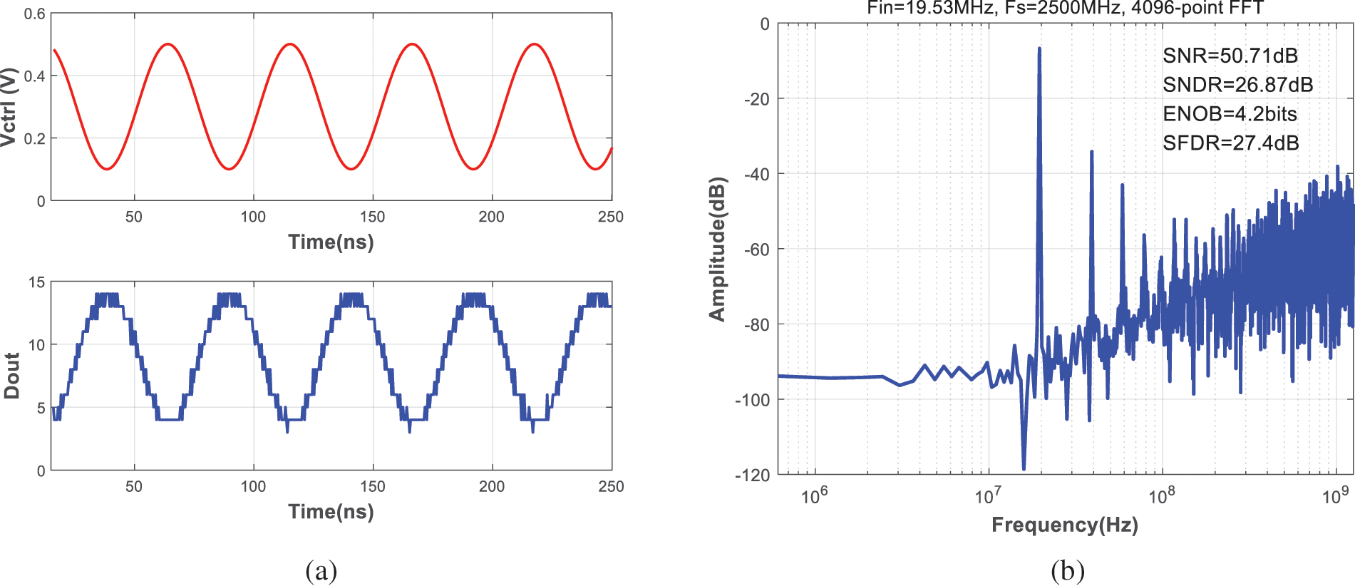
Figure 10: Simulated waveforms (a) and PSD (b) of the proposed PVCOQ for a 19 MHz − 3.5 dBFS input signal
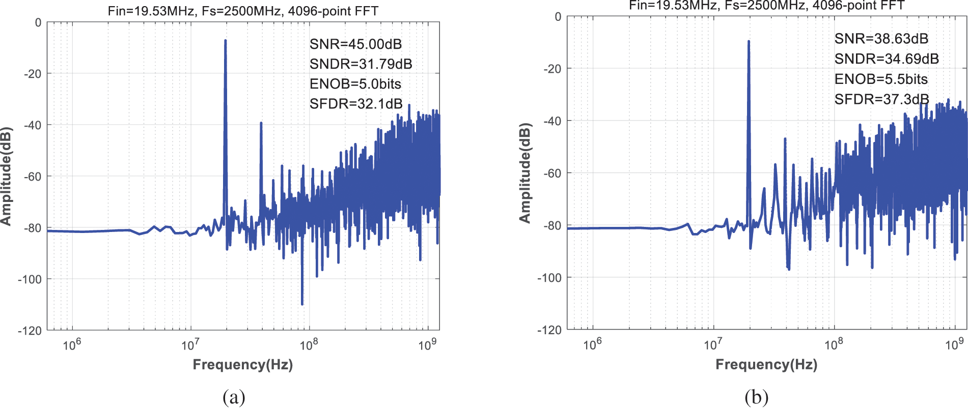
Figure 11: Simulated PSD of the proposed PVCOQ for a 19 MHz − 9.5 dBFS (a) and −15.6 dBFS (b) input signal
4 PVCOQ-SDADC Implementation and Results
The Cascade of Integrators with Feed-Forward Summation (CIFF) structure with a third-order loop filter is adopted, and a 4-bit PVCOQ is used instead of conventional flash quantizer to form PVCOQ-SDADC with an OSR of 16, as shown in Fig. 12. Local resonance is formed by feedback between two integrators, introducing zeros for the noise transfer function, so the noise in-band can be better suppressed.
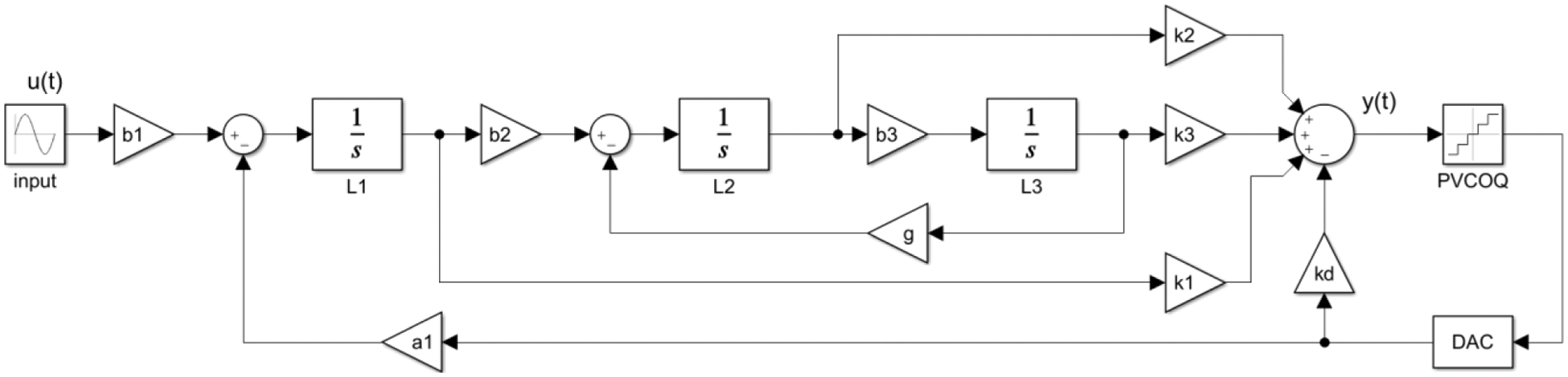
Figure 12: Topology of the proposed PVCOQ-SDADC
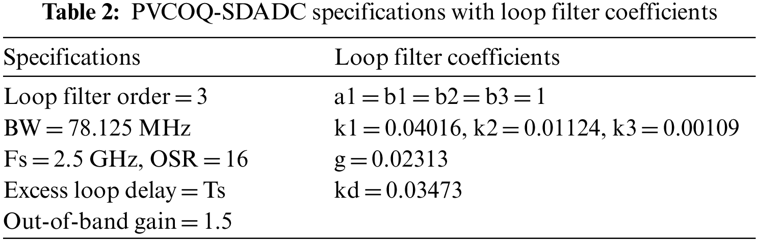
The loop filter coefficients are shown in Tab. 2, calculated by impulse invariance transformation and Matlab SDToolbox [21]. The quantization gain of VCOQ is taken into particular account in the calculation. Note that the coefficients need to be scaled so as not to overload the loop filter.
PVCOQ and flash quantizer are used into SDADC respectively, and the simulated power spectral density is shown in Fig. 13. For the bandwidth of 78.1 MHz, PVCOQ-SDADC suppressed in-band noise more strongly due to its implicit first-order noise-shaping, achieving 92.9 dB SNR and 17.3 dB higher than that of conventional SDADC with flash quantizer.
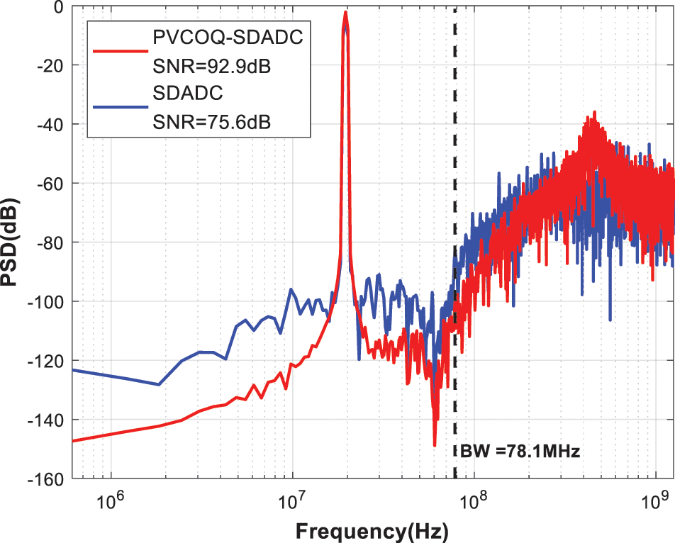
Figure 13: Simulated PSD for a 19 MHz − 2 dBFS input signal for the proposed PVCOQ-SDADC and the conventional SDADC
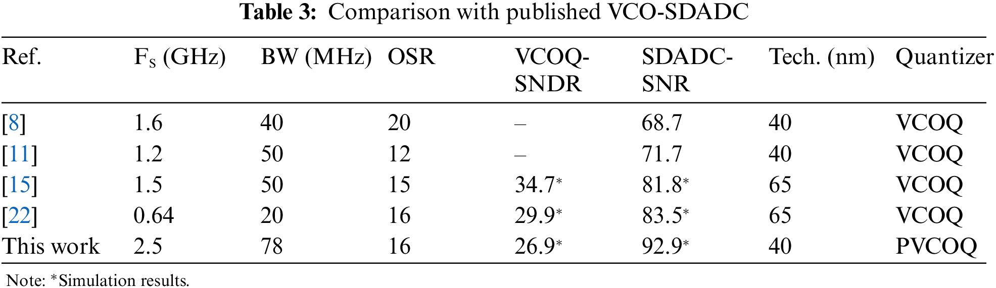
Tab. 3 compares this work with other published VCOQ-SDADC operating at an OSR around 16, where VCOQ-SNDR are the simulation results of VCOQ for −3 dBFS input signal of [15], −7.7 dBFS input signal of [22] and −3.5 dBFS input signal of this work, respectively. The proposed PVCOQ-SDADC shows the similar performance, but has the obvious advantage of digital programmable technique for wider bandwidth.
A high-speed SDADC based on programmable VCOQ is proposed. Due to the intrinsic first-order noise-shaping of the VCO quantizer, the proposed third-order VCOQ-SDADC can realize forth-order noise-shaping ideally. A 4-bit PVCOQ is modeled in Simulink, achieving simulated SNR 55.0 dB very close to the ideal SNR of the first-order conventional SDADC. The proposed PVCOQ, which is designed by analog-digital mixed circuits in 40 nm CMOS technology, consists of an analog VCO circuit and a digital quantizer programmed in Verilog HDL, achieving 50.7 dB SNR, 26.9 dB SNDR and 27.4 dB SFDR for a 19 MHz − 3.5 dBFS input signal in 78 MHz BW. The presented PVCOQ-SDADC operates at 2.5 GHz and achieves behavioral simulation performance of 92.9 dB SNR over 78 MHz BW. The digital programmable structure of the proposed PVCOQ-SDADC can not only greatly shorten the design cycle, but also improve the anti-interference ability, easy to integrate digital circuits.
Acknowledgement: The authors would like to thank K. Yang, R. C. Zhu, P. S. Gu and C. S. Dai for many helpful technical discussions.
Funding Statement: This work was supported by the Natural Science Foundation of the Jiangsu Higher Education Institutions of China under Grant No. 18KJB510045.
Conflicts of Interest: The authors declare that they have no conflicts of interest to report regarding the present study.
1. D. Dangi, A. Bhagat and D. K. Dixit, “Emerging applications of artificial intelligence, machine learning and data science,” Computers, Materials & Continua, vol. 70, no. 3, pp. 5399–5419, 2022. [Google Scholar]
2. R. Krishnamoorthy and K. Krishnan, “Security empowered system-on-chip selection for internet of things,” Intelligent Automation & Soft Computing, vol. 30, no. 2, pp. 403–418, 2021. [Google Scholar]
3. M. H. Alsharif, M. A. Albreem, A. A. Solyman and S. Kim, “Toward 6G communication networks: Terahertz frequency challenges and open research issues,” Computers, Materials & Continua, vol. 66, no. 3, pp. 2831–2842, 2021. [Google Scholar]
4. A. Ghosh and S. Pamarti, “Linearization through dithering: A 50 MHz bandwidth, 10-b ENOB, 8.2 mW VCO-based ADC,” IEEE Journal of Solid-State Circuits, vol. 50, no. 9, pp. 2012–2024, 2015. [Google Scholar]
5. G. Prathiba and M. Santhi, “Design and analysis of 4-bit 1.2gs/s low power CMOS clocked flash ADC,” Intelligent Automation & Soft Computing, vol. 31, no. 3, pp. 1611–1626, 2022. [Google Scholar]
6. J. M. de la Rosa, R. Schreier, K. Pun and S. Pavan, “Next-generation delta-sigma converters: Trends and perspectives,” IEEE Journal on Emerging and Selected Topics in Circuits and Systems, vol. 5, no. 4, pp. 484–499, 2015. [Google Scholar]
7. S. Huang, N. Egan, D. Kesharwani, F. Opteynde and M. Ashburn, “A 125 MHZ-BW 71.9 dB-SNDR VCO-based CT ΔΣ ADC with segmented phase-domain ELD compensation in 16nm CMOS,” in 2017 IEEE International Solid-State Circuits Conf. (ISSCC), San Francisco, CA, USA, pp. 470–471, 2017. [Google Scholar]
8. P. Zhu, X. Xing and G. Gielen, “A 40-MHz bandwidth 0–2 Mash VCO-based delta-sigma ADC with 35-fJ/Step FoM,” IEEE Transactions on Circuits and Systems II: Express Briefs, vol. 62, no. 10, pp. 952–956, 2015. [Google Scholar]
9. L. Xie, Y. Ren, M. Zhou, X. Yang and Z. Huang, “A time-domain comparator based skipping-window SAR ADC,” Computers, Materials & Continua, vol. 69, no. 2, pp. 1597–1609, 2021. [Google Scholar]
10. Y. Zhong, S. Li, A. Sanyal, X. Tang, L. Shen et al., “A second-order purely VCO-based CT ΔΣ ADC using a modified DPLL structure in 40-nm CMOS,” IEEE Journal of Solid-State Circuits, vol. 55, no. 2, pp. 356–368, 2020. [Google Scholar]
11. K. Reddy, S. Dey, S. Rao, B. Young, P. Prabha et al., “A 54 mW 1.2GS/s 71.5 dB SNDR 50 MHz BW VCO-based CT delta sigma ADC using dual phase/frequency feedback in 65 nm CMOS,” in 29th Symp. on VLSI Circuits (VLSI Circuits), Kyoto, JAPAN, pp. C256–C257, 2015. [Google Scholar]
12. M. Baert and W. Dehaene, “A 5-GS/s 7.2-ENOB time-interleaved VCO-based ADC achieving 30.5 fJ/cs,” IEEE Journal of Solid-State Circuits, vol. 55, no. 6, pp. 1577–1587, 2020. [Google Scholar]
13. J. Wang, X. Cheng, J. Han and X. Zeng, “A synthesis friendly VCO-based delta-sigma ADC with process variation tolerance,” in 2020 IEEE International Symp. on Circuits and Systems (ISCAS), Seville, Spain, pp. 1–5, 2020. [Google Scholar]
14. A. Mukherjee, M. Gandara, X. Yang, L. Shen, X. Tang et al., “A 74.5-dB dynamic range 10-MHz BW CT-ΔΣ ADC with distributed-input VCO and embedded capacitive-π network in 40-nm CMOS,” IEEE Journal of Solid-State Circuits, vol. 56, no. 2, pp. 476–487, 2021. [Google Scholar]
15. S. Dey, K. Reddy, K. Mayaram and T. S. Fiez, “A 50 MHz BW 76.1 dB DR two-stage continuous-time delta–sigma modulator with VCO quantizer nonlinearity cancellation,” IEEE Journal of Solid-State Circuits, vol. 53, no. 3, pp. 799–813, 2018. [Google Scholar]
16. M. Z. Straayer and M. H. Perrott, “A 10-bit 20 MHz 38 mW 950 MHz CT ΣΔ ADC with a 5-bit noise-shaping VCO-based quantizer and DEM circuit in 0.13u CMOS,” in 2007 IEEE Symposium on VLSI Circuits, Kyoto, Japan, pp. 246–247, 2007. [Google Scholar]
17. M. Z. Straayer and M. H. Perrott, “A 12-Bit, 10-MHz bandwidth, continuous-time ΣΔ ADC with a 5-Bit, 950-MS/s VCO-based quantizer,” IEEE Journal of Solid-State Circuits, vol. 43, no. 4, pp. 805–814, 2008. [Google Scholar]
18. H. Sun, J. Muhlestein, S. Leuenberger, K. Sobue, K. Hamashita et al., “A 50 MHz bandwidth 54.2 dB SNDR reference-free stochastic ADC using VCO-based quantizers,” in 2016 IEEE Asian Solid-State Circuits Conference (A-SSCC), Toyama, Japan, pp. 325–328, 2016. [Google Scholar]
19. A. Iwata, N. Sakimura, M. Nagata and T. Morie, “An architecture of delta-sigma A-to-D converters using a voltage controlled oscillator as a multi-bit quantizer,” in 1998 IEEE International Symp. on Circuits and Systems, Monterey, CA, USA, pp. 389–392, 1998. [Google Scholar]
20. J. Kim and S. Cho, “A time-based analog-to-digital converter using a multi-phase voltage controlled oscillator,” in 2006 IEEE International Symp. on Circuits and Systems, Kos, Greece, pp. 3934–3937, 2006. [Google Scholar]
21. S. Pavan, “Systematic design centering of continuous time oversampling converters,” IEEE Transactions on Circuits and Systems II: Express Briefs, vol. 57, no. 3, pp. 158–162, 2010. [Google Scholar]
22. H. Chen, “Research on key technologies of low power continuous time sigma-delta modulator,” M.S. dissertation, Xidian University, China, 2019. [Google Scholar]
 | This work is licensed under a Creative Commons Attribution 4.0 International License, which permits unrestricted use, distribution, and reproduction in any medium, provided the original work is properly cited. |