DOI:10.32604/cmc.2022.026831
| Computers, Materials & Continua DOI:10.32604/cmc.2022.026831 | |
| Article |
CNTFET Based Grounded Active Inductor for Broadband Applications
1Department of Electrical Engineering, Umm Al Qura University, Makkah, 21955, Saudi Arabia
2School of Electrical Engineering, Faculty of Engineering, Universiti Teknologi Malaysia, Johor Bahru, 81310, Johor, Malaysia
*Corresponding Author: Muhammad I. Masud. Email: mimasud@uqu.edu.sa
Received: 05 January 2022; Accepted: 14 April 2022
Abstract: A new carbon nanotube field effect transistor (CNTFET) based grounded active inductor (GAI) circuit is presented in this work. The suggested GAI offers a tunable inductance with a very wide inductive bandwidth, high quality factor (QF) and low power dissipation. The tunability of the realized circuit is achieved through CNTFET based varactor. The proposed topology shows inductive behavior in the frequency range of 0.1–101 GHz and achieves to a maximum QF of 9125. The GAI operates at 0.7 V with 0.337 mW of power consumption. To demonstrate the performance of GAI, a broadband low noise amplifier (LNA) circuit is designed by utilizing the GAI based input matching-network. The realized LNA provides high frequency bandwidth (17.5–57 GHz), low noise figure (<3 dB) and occupies less space due to absence of any spiral inductor. Moreover, it exhibits a flat forward gain of 15.9 ± 0.9 dB, a reverse isolation less than −63 dB and input return loss less than −10 dB over the entire frequency bandwidth. The proposed CNTFET based GAI and LNA circuits are designed and verified by using HSPICE simulations with Stanford CNTFET model at 16 nm technology node.
Keywords: Active inductor; gyrator-C; CNTFET; quality factor; self-resonance frequency
Inductors are crucial components of many high frequency analog signal processing (ASP) circuits. They are utilized in LNAs, voltage-controlled oscillators, filters, frequency dividers, impedance matching-networks and phase shifters to name a few [1]. However, their implementation in integrated circuits (ICs) is a challenging task. An on-chip spiral inductor dominates the die area of the IC, resulting in higher fabrication cost and also presents several disadvantages such as low QF, fixed inductance value and incompatibility with semiconductor fabrication process [2,3]. Limitations of spiral on-chip inductor motivates IC designers to opt for active-circuitry for synthesizing the integrated inductors. Comparatively to spiral inductor, an active inductor (AI) offers high tunable inductance, high QF and it requires smaller area [4]. However, AIs consume large power and introduce noise [5].
From technical literature, several GAI topologies have been reported by employing high performance active building blocks (ABBs) like extra-X current controlled current conveyor [6], differential difference current conveyor [7], current feedback operational amplifier [8], current differencing buffered amplifier [9], voltage differencing inverting buffered amplifier [10], inverting voltage buffer [11], dual-X current conveyor transconductance amplifier [12] and four terminal floating nullor transconductance amplifier [13]. However, high frequency performance of these GAI topologies is limited due to low self-resonance frequency (SRF), large number of active and passive devices, high power consumption and large chip area.
Several gyrator-C based compact GAI topologies, utilizing positive transconductance element (PTE) and negative transconductance element (NTE) as an ABB can be found in the technical literature [1–3,5,14–22]. However, each of these GAI topologies offers a few desirable specifications such as low power dissipation, wide inductance bandwidth, high QF, large tunable inductance, low noise and ability to work on low voltages. Although most AI circuit topologies presented to date are compact and achieve acceptably larger QF than its spiral counterpart, their application in low voltage, low power broadband ASP modules has been limited because of their narrow inductive bandwidth. As a result, to the best of authors knowledge, AI circuit topology has so far not been utilized in high frequency applications (>11 GHz) and wideband (>7 GHz bandwidth) ASP modules [3]. This comparatively limited inductive bandwidth ultimately reduced their feasibility for the design of broadband high frequency ASP modules.
It is to be noted that GAI topologies proposed in the technical literature [1–3,5–22] are based on bulk semiconductor technology. However, this technology faces numerous challenges below 22 nm technology node [23]. The issues include high field effects, short channel control, increased leakage, boron penetration, polysilicon depletion, direct gate tunneling current and lithographic limitations [24–27]. Therefore, it is extremely imperative for IC designers to explore new materials and devices for below 22 nm node, that equally works well to keep Moore’s law alive [23].
To find replacements for CMOS technology, many devices and techniques are being introduced and evaluated by researchers such as double gate field effect transistors (FETs), single electron transistor, fin FETs and CNTFET [25]. Among these solutions, the CNTFET has tremendous potential to further continue the feature length down-scaling and extend Moore’s law, due to its near ballistic transport of charge carriers, large thermal conductivity, higher cutoff frequency, smaller size, fast switching speed and low parasitic capacitances [26]. These excellent CNTFET features lead it as a suitable candidate for multi GHz frequency applications. Since CNTFET introduction as an alternative to MOSFET, limited studies on CNTFET based AI has been carried out [27]. However, the reported CNTFET based GAI topology utilizes large number of active and passive devices and suffers from low SRF, large chip area and high power dissipation.
In this work, a wide tunable CNTFET based GAI circuit is presented. The realized GAI circuit uses recently proposed PTE along with NTE as an ABB and one CNTFET varactor [28]. Tunability of GAI is achieved through the CNTFET varactor. The proposed GAI circuit enjoys higher tunable inductance magnitude over a very wide frequency band along with high QF, high SRF and low power dissipation. To evaluate the performance of the GAI topology, the proposed circuit is utilized in LNA. The GAI based LNA provides high frequency bandwidth, high gain, low noise figure (NF) and low power dissipation. The realized CNTFET based GAI has been studied in detail and the design is validated with HSPICE simulations by utilizing Stanford model [29].
Subsequent sections are organized as follows. Section 2 discusses CNTFET in detail. The GAI circuit description is given in Section 3. Simulation results of the realized CNTFET based GAI are elaborated in Section 4. Comparison of the proposed GAI with other topologies is presented in Section 5. The application of GAI is demonstrated in Section 6. Lastly, the conclusion is provided in Section 7.
2 Carbon Nanotube Field Effect Transistor
Carbon nanotube (CNT), an allotrope of carbon, are graphite cylindrical sheets (GCS) which are rolled into cylindrical shape with diameter in the range of 1 to 50 nm and length of a few micrometers. CNTs are considered as the most attractive nanomaterial for future ASP applications due to its extraordinary electrical, chemical, mechanical, optoelectronics, and thermal properties [23]. CNTFET is an important application of CNT. It is realized by replacing the MOSFET conventional channel with an array of isolated and aligned single wall CNTs. The CNTs behave as the medium of conduction between the drain and source terminals as shown in Fig. 1. Like MOSFET, CNTFET also works as a voltage controlled active device. The CNTFET channel current is controlled through gate terminal voltage. CNTFET gate is coupled capacitively with the underneath channel that utilizes one or more CNTs [24]. In comparison to MOSFET, CNTFET enjoys numerous outstanding advantages like higher temperature resilience, larger transconductance, larger driving current, one-dimensional ballistic transport capability, near ideal subthreshold slope and lower value of intrinsic capacitances [25,26].
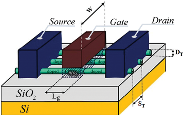
Figure 1: CNTFET 3D view
The geometric parameters ST, DT, NT and W are the inter-CNT pitch, CNT diameter, number of channels and the transistor gate width respectively. These parameters are important for performance optimization of CNTFET. The parameter DT and threshold voltage (Vth) of a single wall CNT are given by following equations [30].
where n and m are the chiral vectors, ac is the graphene lattice constant, Eg is the band gap energy and q is the electron charge. The CNTFET gate width is given by following equation [24]:
Thus, the width of CNTFET can be adjusted by selecting ST, DT and NT values to optimize the circuit performance.
The proposed GAI topology with its equivalent RLC circuit is shown in Fig. 2. It is based on gyrator-C topology. CNTFETs T1 and T4 form the NTE and CNTFETs T2, T3, T5 and T6 constitute the PTE [28]. The PTE utilizes CNTFETs T2 and T5 as an inverting voltage buffer (IVB) [24]. The varactor Cvar utilized in Fig. 2 is based on a single CNTFET, as shown in Fig. 3 [25]. The CNTFET based varactor drain and source are tied together and then connected to control voltage Vtune. The varactor capacitance Cvar can be controlled by varying Vtune. Fig. 4 demonstrate the small signal equivalent circuit of the GAI. In Fig. 4, each CNTFET is presented by gmi, gdsi and Cgsi which are the transconductance, output conductance and gate to source capacitance of the i-th transistor respectively. For simplicity, Cgd is neglected (since Cgd << Cgs).
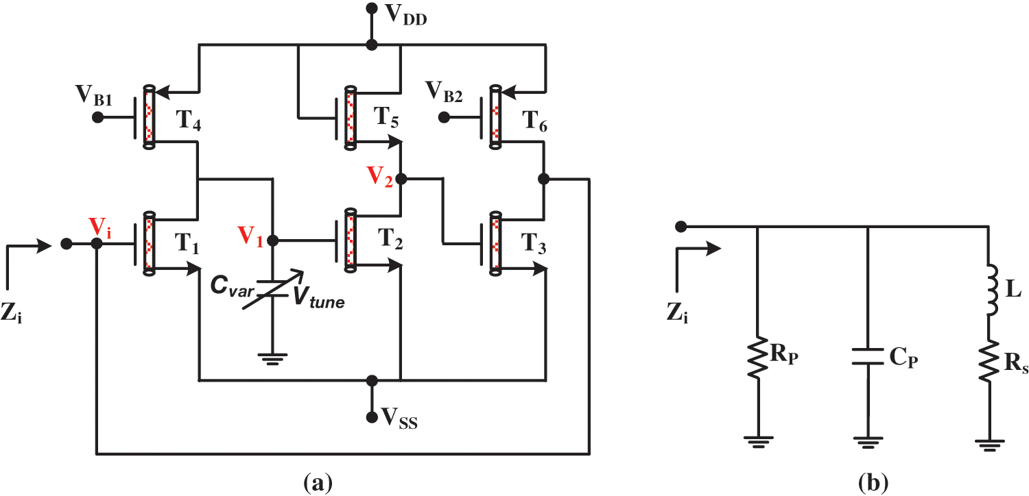
Figure 2: Active inductor (a) proposed circuit (b) equivalent RLC circuit
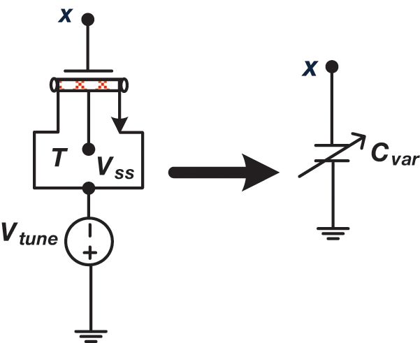
Figure 3: Varactor transistor level realization with its symbol
By using the small signal equivalent model of Fig. 4, the input admittance (Yi = 1/Zi = Ii/Vi) can be found as.
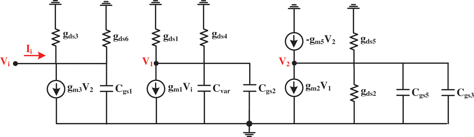
Figure 4: GAI small signal equivalent circuit
where the parameter α, β,
By considering gm5 >> gds2, gm5 >> gds5, gm5 >> gds1, gm5 >> gds4, Cvar >> Cgs3, and Cvar >> Cgs5, the equivalent RLC circuit model components of Fig. 2b can be derived as:
It can be seen from Eq. (13) that inductance of GAI can be controlled by adjusting the capacitance of CNTFET varactor. Thus, increasing the value of Vtune of CNTFET varactor, will increase the magnitude of inductance L. Moreover, the transconductance ratio of IVB (gm5/gm2), also plays a vital role in the improvement of inductance magnitude. The QF relation derived from the RLC equivalent circuit of Fig. 2 is given by:
The SRF of GAI which determine the circuit inductive behavior upper limit in frequency band can be written as:
By analyzing Eqs. (13) and (15), it is seen that a tradeoff exists between the GAI inductance magnitude and SRF. With higher transconductance of CNTFET T5, a significant increase in the inductance value can be achieved but the inductance bandwidth will shrink accordingly. The realized GAI utilizes few number of transistors in the main path of signal, which made it suitable for high frequency broadband applications. Moreover, the designed GAI is suitable for low voltage operation as it employs only two CNTFETs between its supply rails. In addition, it is suitable for integration due to absence of any external passive component.
The proposed GAI of Fig. 2 is designed and verified using HSPICE simulation tool with supply voltages VDD = 0.7 V and VSS = −0.7 V. All the transistors are modeled using Stanford CNTFET model with transistor parameters mentioned in Tab. 1. The diameter DT is set to 3 nm for GAI design. Moreover, with constant pitch ST = 10 nm, the major design factor of the CNTFET based GAI is the parameter NT. In this regard, the transconductance ratio gm5/gm2 is almost equal to NT5/NT2.
The proposed topology is simulated using CNTFET parameters of Tab. 1 along with NT1 = 5, NT2 = 5, NT3 = 5, NT4 = 5, NT5 = 30, NT6 = 5 and NT7 = 157. Initially the varactor tuning voltage Vtune is set to −0.60 V. Figs. 5a and 5b show the magnitude and phase response of GAI input impedance. From Figs. 5a and 5b, a high SRF equivalent to 101 GHz is observed. Fig. 5c shows the GAI inductance plot. The inductance ranges from nearly 47.8 nH to 287.4 nH and can be adjusted to a set value for a specific frequency range. The AI circuit behavior is dominantly inductive in the frequency band, ranging from approximately 0.1 GHz to 101 GHz. The peak inductance value is found at 96.6 GHz. This wide inductive bandwidth makes the proposed GAI an attractive choice for broadband high frequency applications. Fig. 5d shows the GAI QF plot. The maximum QF obtained is equivalent to 9125 at 16.6 GHz. This high QF is another advantage of the proposed work. The power dissipation is 0.337 mW. The realized GAI dissipates very small power, even at very high frequency of operation. The equivalent input referred noise for the circuit is 21.5 nV/√Hz, which is adequately a low value.
Figure 5: GAI frequency response (a) Zin magnitude (b) Zin phase (c) inductance (d) QF
The main criterion for selecting an AI for analog system design is its ability to tune to different resonant frequencies. As depicted by Eq. (13), the GAI inductance can be controlled by varying varactor capacitance Cvar. To demonstrate the proposed GAI tunability feature, different tuning voltages Vtune are applied to the varactor. Fig. 6 shows the magnitude response of GAI input impedance, at different values of Vtune. It can be seen that the input impedance frequency band can be tuned to different frequencies by altering Vtune. The SRF are found as 101.2 GHz, 131.8 GHz, 160.3 GHz, 245.5 GHz, 319.9 GHz for Vtune equal to −0.60 V, −0.38 V, −0.35 V, −0.30 V, −0.15 V respectively. By varying the Vtune from −0.60 V to −0.15 V the GAI input impedance magnitude decreases from 351.7 kΩ to 34.4 kΩ. This tunable input impedance over a large frequency band makes the proposed work suitable for multi GHz ASP applications.
Figure 6: Frequency response of Zin magnitude at different values of Vtune
Fig. 7 shows the frequency response of GAI inductance, at different values of Vtune. The maximum inductance is achieved at −0.60 V, where the inductance value varies in the range of 47.8 nH to 287.4 nH with a SRF of 101 GHz. The minimum inductance is achieved at −0.15 V, where the inductance value varies in the range of 4.4 nH to 9.6 nH with a SRF of 319.9 GHz. It can be seen that a tradeoff exists between the inductance magnitude and inductive bandwidth/SRF. Fig. 8a shows the variation of GAI inductance vs. varactor tuning voltage Vtune at a fixed frequency of 40 GHz. Fig. 8b demonstrates the variation of SRF versus Vtune. As discussed earlier, a trade-off exists between the inductive bandwidth/SRF and inductance magnitude, which is more obvious from Fig. 8.
Figure 7: Frequency response of GAI inductance at different values of Vtune
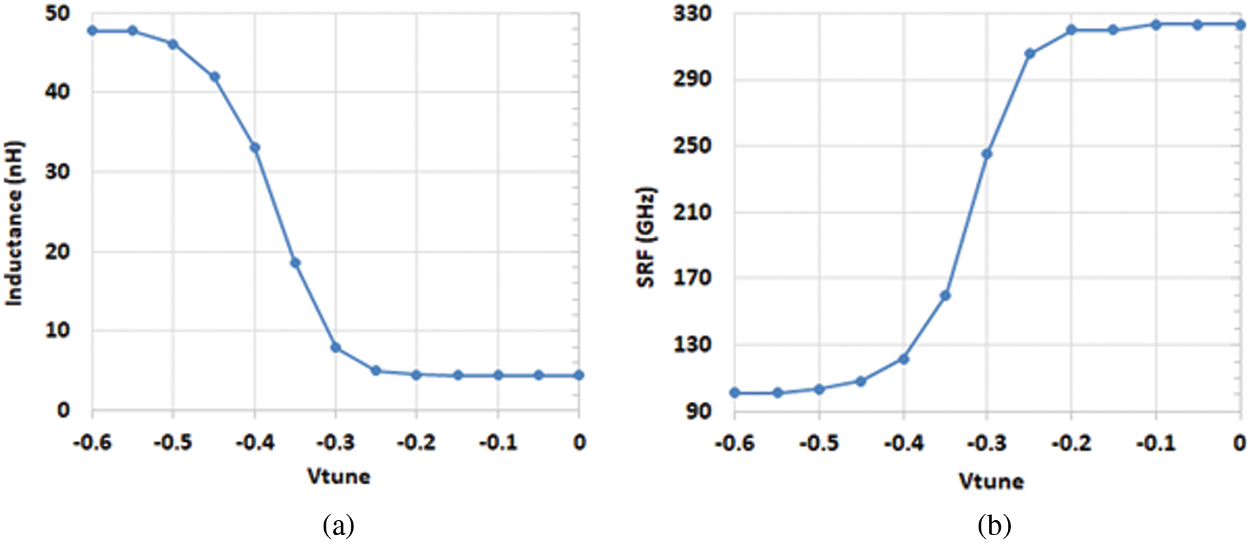
Figure 8: GAI (a) inductance versus Vtune (b) SRF versus Vtune
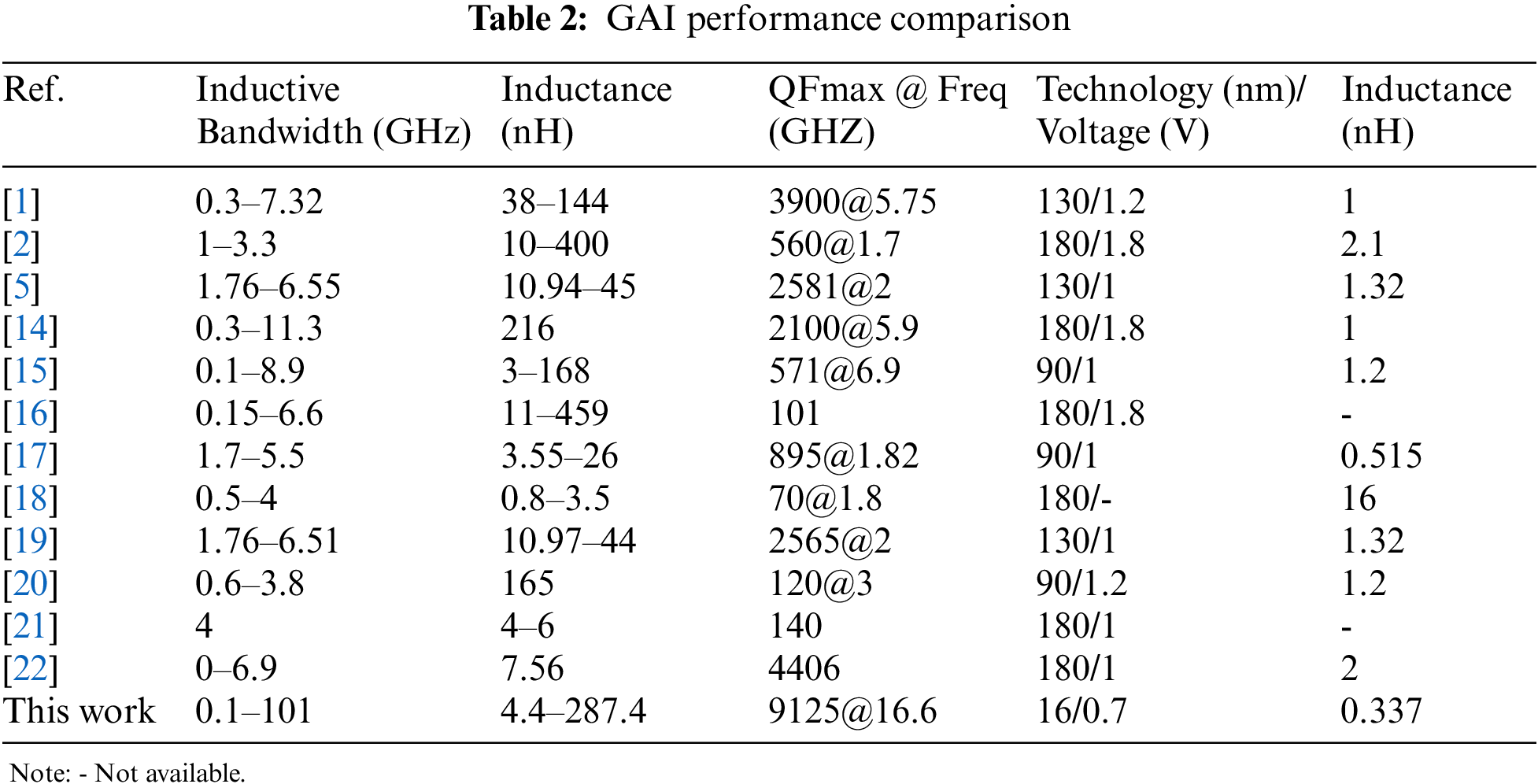
Tab. 2 summarizes a comparison of the realized GAI circuit with some other gyrator-C based AI topologies in the technical literature [1–2,5,14–22]. Except for the proposed topology, which is in CNTFET, the other GAI topologies are based on CMOS technology. For comparison, only GAI circuits suitable for multi-GHz ASP applications are included in Tab. 2. Limited works on CNTFET based GAI topology are available in the technical literature [27], however its frequency of operation is limited to MHz range. The GAI performance is compared for the characteristic’s parameters inductive bandwidth, maximum inductance, maximum QF and power dissipation. Comparison results demonstrate that the realized GAI has maximum inductive bandwidth, highest QF, minimum power consumption, and large inductance. The inductive bandwidth of the proposed work is almost 9 times greater than [14]. The QF of the proposed work is almost 2 times greater than [22]. In comparison to [17], the proposed GAI shows 34% reduction in power dissipation.
In this section, the application of the proposed CNTFET GAI is demonstrated. The proposed GAI is utilized in the dual negative feedback common gate (DNFCG) LNA topology [31]. For matching-network, LNA topologies usually utilize on chip passive spiral inductors. From Fig. 9a, it can be seen that spiral inductor Lbiase is utilized by DNFCG LNA topology for matching. However, this inductor suffers from many drawbacks like low SRF, low QF, fixed and low inductance magnitude, larger chip area and incompatibility with standard CNTFET/CMOS technology. It is then most preferable to utilize AI instead of bulky spiral inductor, for reducing cost and size of LNAs.
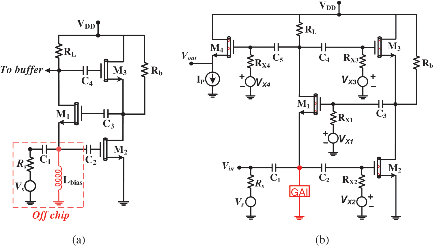
Figure 9: (a) DNFCG LNA [31] (b) GAI based DNFCG LNA
Fig. 9b shows the complete GAI based DNFCG LNA, where passive inductor Lbiase of Fig. 9a is replaced with the proposed GAI circuit. The common gate impedance matching transistor M1, amplifies the input and provides the main forward signal path. The common source transistor M2 along with resistor Rb forms the inverting gain block between M1 source and gate terminals and thus help in boosting the transconductance of M1. Resistor Rb sets the loop gain and supplies the difference in bias current between the source follower transistor M3 and M2. The source follower transistor M4 works as a buffer. The coupling capacitors C1, C2, C3, C4, C5 and bias resistors Rx1, Rx2, Rx3, Rx4 form the bias-network for the respective transistors. For proper operation of GAI based LNA, the zero frequency-ωz and the pole frequency-ωp of the utilized GAI, should be equal to the lowest and highest operating frequency, respectively.
The input impedance of Fig. 9 can be derived as:
where Cp is the total parasitic capacitance at the input due to transistor M1 and M2. The input matching-network is thus a parallel resonance, where GAI can be used to cancel the capacitive effects at the input-terminal. Thus, the parasitic Cp is absorbed into the LC-network and the imaginary part of Zin is insignificant within the intended bandwidth [3,31]. The voltage gain A can be calculated as.
By assuming gm3 << gm2 and gm3Rb(gm1RL + 1) <<1, Eq. (17) can be reduced to:
The total NF is given by following relation.
where Hmi are the CNTFET coefficients with magnitude less than one [30]. The LNA circuit with gain much greater than unity will reduce the noise impact of Rb and transistors M1, M2, M3, M4 on the NF. Tab. 3 shows the important design parameters for DNFCG LNA. It is to be noted that the NT2 of Common source transistor M2 is set to sufficiently greater than NT3 to fulfill the primary assumptions [gm3Rb(gm1RL + 1)] <<1 and gm3 << gm2. For GAI the CNTFET parameters of Tab. 1 are used along with NT7 = 157, NTi = 10, where NT7 is the number of tubes of the CNTFET varactor T7 and NTi is the number of tubes utilized by all other CNTFETs.
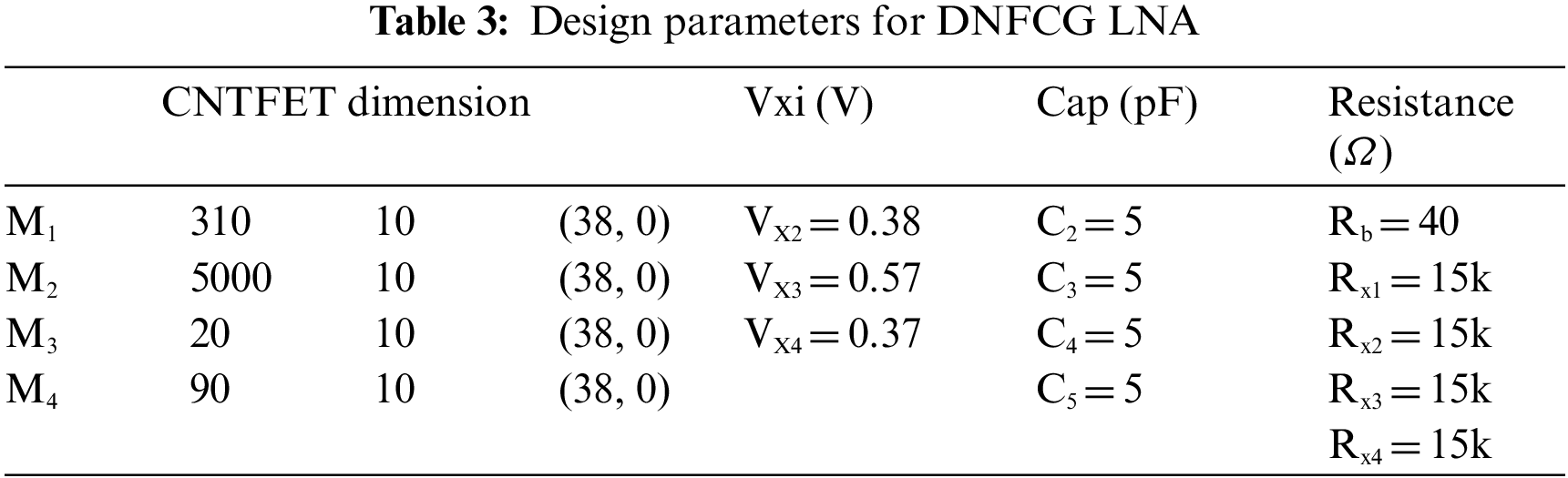
Fig. 10 shows the forward-gain (S21) and NF. It can be seen that the simulated gain is equivalent to 15.9 dB over the frequency range of 17.5 GHz to 57 GHz and drops by just 0.9 dB over the entire bandwidth. One of the important design considerations of broadband LNA is to keep the NF magnitude lower than 3 dB for frequency range of interest. It can be seen that over the entire bandwidth (17.5 GHz to 57 GHz), the NF magnitude is less than 3 db.
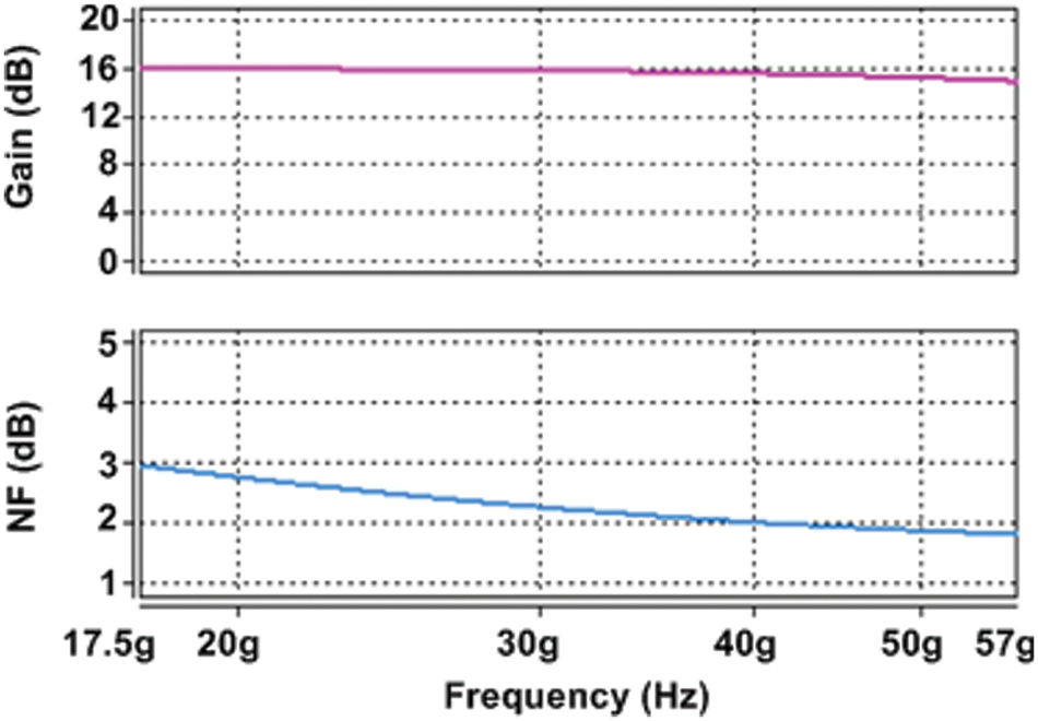
Figure 10: GAI based LNA gain and NF versus frequency
Fig. 11 demonstrates the S11, S12 and S22 simulation results for the realized GAI based LNA. Magnitude of S11 ranges from −16.8 dB to −11.4 dB over the bandwidth (17.5 GHz to 57 GHz). The power dissipation of GAI based LNA is 6.961 mW. In summary, the realized GAI based LNA provides very high frequency bandwidth (17.5 GHz to 57 GHz), low NF (<3 dB), occupy less space due to absence of any spiral inductor and consumes only 6.961 mW.
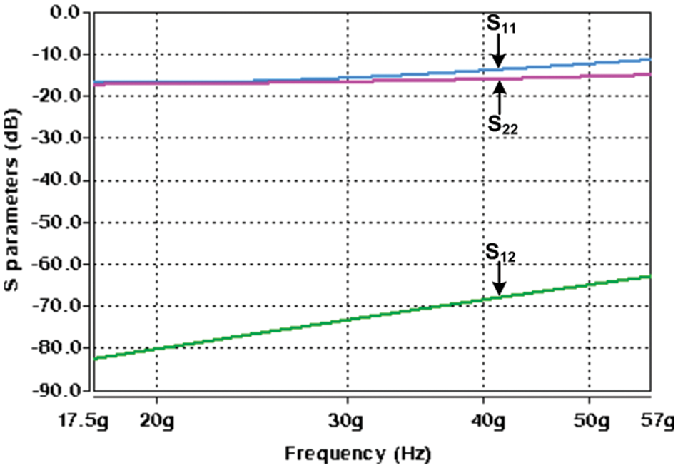
Figure 11: S11, S12 and S22 versus frequency
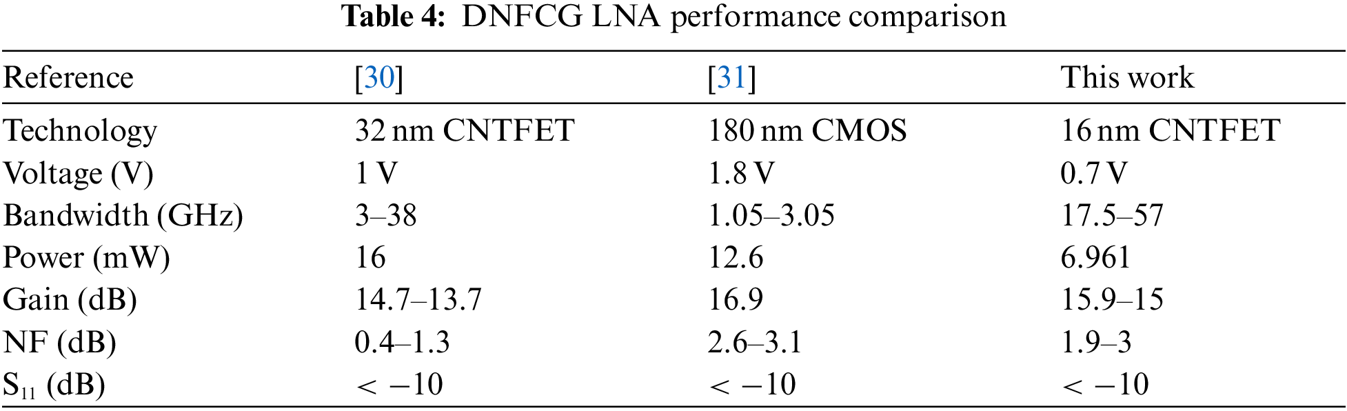
Tab. 4 demonstrates the comparison of proposed CNTFET GAI based DNFCG LNA with other DNFCG LNA topologies. It can be seen that GAI based LNA design offers larger bandwidth and lower power dissipation. It is also important to mention that the tunability feature of GAI is useful for compensating the undesirable parameter effects due to process, voltage, temperature variations. Moreover, it can easily help to adopt specification of other broadband high frequency ASP applications. Due to wide inductive bandwidth, high QF, low power dissipation and large tunable inductance, the proposed GAI circuit can be utilized as a potential candidate for 5G/6G communication ASP modules.
In this work, a CNTFET based GAI is presented. The proposed GAI circuit is free from external passive components and thus it is suitable for integrated circuit implementation. The realized AI is based on gyrator-C topology and employs only a few CNTFETs in the main path of signal which made it suitable for multi GHz broadband ASP applications. Simulation results demonstrate that the realized circuit consumes small power and provides high inductance, high QF, and large inductive bandwidth. These advantages make the proposed GAI an attractive candidate for low power, low voltage and high frequency broadband applications. Application of GAI is demonstrated in the design of broadband CNTFET based DNFCG LNA. Using the realized GAI in the input matching-network reduces the chip area. The realized GAI based LNA provides high gain, high frequency bandwidth, low NF and low power dissipation. The GAI and LNA circuit simulation outcomes based on CNTFET Stanford model using 16 nm technology node confirm the theoretical predictions.
Funding Statement: The authors would like to thank the Deanship of Scientific Research at Umm Al-Qura University for supporting this work by Grant Code: (22UQU4320299DSR01).
Conflicts of Interest: The authors declare that they have no conflicts of interest to report regarding the present study.
1. H. U. Uyanik and N. Tarim, “Compact low voltage high-Q CMOS active inductor suitable for RF applications,” Analog Integrated Circuits and Signal Processing, vol. 51, no. 3, pp. 191–194, 2007. [Google Scholar]
2. H. B. Kia and A. K. A’ain, “A wide tuning range voltage controlled oscillator with a high tunable active inductor,” Wireless Personal Communication, vol. 79, no. 1, pp. 31–41, 2014. [Google Scholar]
3. A. Saberkari, S. Kazemi, V. Shirmohammadli and M. C. Yagoub, “Gm-boosted flat gain UWB low noise amplifier with active inductor-based input matching network,” Integration, vol. 52, pp. 323–333, 2016, https://doi.org/10.1016/j.vlsi.2015.06.002. [Google Scholar]
4. W. Jaikla, S. Bunrueangsak, F. Khateb, T. Kulej, P. Suwanjan et al., “Inductance simulators and their application to the 4th order elliptic lowpass ladder filter using CMOS VD-DIBAs,” Electronics, vol. 10, no. 6, pp. 684, 2021. [Google Scholar]
5. A. B. Hammadi, M. Mhiri, F. Haddad, S. Saad and K. Besbes, “An enhanced design of multi-band RF band pass filter based on tunable high-Q active inductor for nano-satellite applications,” Journal Circuits System and Computers, vol. 26, no. 4, pp. 1750055, 2017. [Google Scholar]
6. D. Agrawal and S. Maheshwari, “Electronically tunable grounded immittance simulators using an EX-CCCII,” International Journal of Electronics, vol. 107, no. 10, pp. 1625–1648, 2020. [Google Scholar]
7. A. Abaci and E. Yuce, “Single DDCC based new immittance function simulators employing only grounded passive elements and their applications,” Microelectronics Journal, vol. 83, pp. 94–103, 2019. [Google Scholar]
8. M. Dogan and E. Yuce, “CFOA based a new grounded inductor simulator and its applications,” Microelectronics Journal, vol. 90, pp. 297–305, 2019. [Google Scholar]
9. J. K. Pathak, A. K. Singh and R. Senani, “New canonic lossy inductor using a single CDBA and its application,” International Journal of Electronics, vol. 103, no. 1, pp. 1–13, 2016. [Google Scholar]
10. W. Tangsrirat. “Synthetic grounded lossy inductance simulators using single VDIBA,” IETE Journal of Research, vol. 63, no. 1, pp. 134–141, 2017, https://doi.org/10.1080/03772063.2016.1221746. [Google Scholar]
11. A. Yesil, E. Yuce and S. Minaei, “Inverting voltage buffer based lossless grounded inductor simulators,” AEU-International Journal of Electronics and Communications, vol. 83, pp. 131–137, 2018. [Google Scholar]
12. N. Kumar, J. Vista and A. Ranjan, “A tuneable active inductor employing DXCCTA: Grounded and floating operation,” Microelectronics Journal, vol. 90, pp. 1–11, 2019. [Google Scholar]
13. H. Tarunkumar, S. Shantikumar and A. Ranjan, “An active inductor employing a new four terminal floating nullor transconductance amplifier (FTFNTA),” International Journal of Electronics, vol. 107, no. 5, pp. 683–702, 2020. [Google Scholar]
14. H. G. Momen, M. Yazgi, R. Kopru and A. N. Saatlo, “Low-loss active inductor with independently adjustable self-resonance frequency and quality factor parameters,” Integration, vol. 58, pp. 22–26, 2017. [Google Scholar]
15. H. G. Momen, M. Yazgi and R. Kopru, “A low loss, low voltage and high Q active inductor with multi-regulated cascade stage for RF applications,” in Proc. of IEEE Int. Conf. on Electronics, Circuits, and Systems (ICECS), Cairo, Egypt, pp. 149–152, 2015. [Google Scholar]
16. J. Manjula and S. Malarvizhi, “Active inductor based tunable multiband RF front end design for UWB applications,” Analog Integrated Circuits and Signal Processing, vol. 95, no. 2, pp. 195–207, 2018, https://doi.org/10.1007/s10470-018-1168-7. [Google Scholar]
17. S. Saad, M. Mhiri, A. B. Hammadi and K. Besbes, “A new low-power, high-Q, wide tunable CMOS active inductor for RF applications,” IETE Journal of Research, vol. 62, no. 2, pp. 265–273, 2016. [Google Scholar]
18. R. Bhattacharya, A. Basu and S. K. Koul, “A highly linear CMOS active inductor and its application in filters and power dividers,” IEEE Microwave and Wireless Components Letters, vol. 25, no. 11, pp. 715–717, 2015. [Google Scholar]
19. M. Mhiri, A. B. Hammadi, F. Haddad, S. Saad and K. Besbes, “Power and noise optimization techniques of RF active inductor using multi-finger gate transistors,” BioNanoScience, vol. 8, pp. 264–271, 2018, https://doi.org/10.1007/s12668-017-0483-2. [Google Scholar]
20. S. V. Krishnamurthy, K. El-Sankary and E. El-Masry, “Noise-cancelling CMOS active inductor and its application in RF band-pass filter design,” International Journal of Microwave Science and Technology, vol. 2010, pp. 1–8, 2010, https://doi.org/10.1155/2010/980957. [Google Scholar]
21. M. Nair, Y. Zheng and Y. Lian, “1 V, 0.18 μm-area and power efficient UWB LNA utilising active inductors,” Electronics Letters, vol. 44, no. 19, pp. 1127–1129, 2008. [Google Scholar]
22. A. Saberkari, S. Ziabakhsh, H. Martinez and E. Alarcón, “Active inductor-based tunable impedance matching network for RF power amplifier application,” Integration, vol. 52, pp. 301–308, 2016, https://doi.org/10.1016/j.vlsi.2015.07.013. [Google Scholar]
23. S. Jogad, S. A. Loan, N. Afzal and A. G. Alharbi, “CNTFET based class AB current conveyor II: Design, analysis and waveform generator applications,” International Journal of Numerical Modelling: Electronic Networks, Devices and Fields, vol. 34, no. 1, pp. 1–15, 2021, https://doi.org/10.1002/jnm.2783. [Google Scholar]
24. M. I. Masud, A. K. A’ain, I. A. Khan and N. Shaikh-Husin, “A CNTFET-C first order all pass filter,” Analog Integrated Circuits and Signal Processing, vol. 100, no. 2, pp. 257–268, 2019. [Google Scholar]
25. M. Masud, A. A’ain, I. Khan and N. Husin, “Design of voltage mode electronically tunable first order all pass filter in ± 0.7 V 16 nm CNFET technology,” Electronics, vol. 8, no. 1, pp. 1–19, 2019 https://doi.org/10.3390/electronics8010095. [Google Scholar]
26. M. Nizamuddin, S. A. Loan, A. R. Alamoud and S. A. Abbassi, “Design, simulation and comparative analysis of CNT based cascode operational transconductance amplifiers,” Nanotechnology, vol. 26, no. 39, pp. 1–13, 2015, https://doi.org/10.1088/0957-4484/26/39/395201. [Google Scholar]
27. S. Jogad, H. I. Alkhammash, N. Afzal and S. A. Loan, “CNTFET-based active grounded inductor using positive and negative current conveyors and applications,” International Journal of Numerical Modelling: Electronic Networks, Devices and Fields, vol. 34, no. 5, pp. 1–22, 2021, https://doi.org/10.1002/jnm.2895. [Google Scholar]
28. M. I. Masud, A. K. A’ain, I. A. Khan and N. Shaikh-Husin, “CNTFET based voltage mode MISO active only biquadratic filter for multi-GHz frequency applications,” Circuits, Systems, and Signal Processing, vol. 40, no. 10, pp. 4721–4740, 2021, https://doi.org/10.1007/s00034-021-01699-5. [Google Scholar]
29. J. Deng and P. Wong, “A compact SPICE model for carbon-nanotube field-effect transistors including nonidealities and its application—Part II: Full device model and circuit performance benchmarking,” IEEE Transactions on Electron Devices, vol. 54, no. 12, pp. 3195–3205, 2007. [Google Scholar]
30. A. Saberkari, O. Khorgami, J. Bagheri, M. Madec, S. M. Hosseini-Golgoo et al., “Design of broadband CNFET LNA based on extracted I–V closed-form equation,” IEEE Transaction on Nanotechnology, vol. 17, no. 4, pp. 731–42, 2018. [Google Scholar]
31. J. Kim, S. Hoyos and J. Silva-Martinez, “Wideband common-gate CMOS LNA employing dual negative feedback with simultaneous noise, gain, and bandwidth optimization,” IEEE Transactions on Microwave Theory and Techniques, vol. 58, no. 9, pp. 2340–2351, 2010. [Google Scholar]
 | This work is licensed under a Creative Commons Attribution 4.0 International License, which permits unrestricted use, distribution, and reproduction in any medium, provided the original work is properly cited. |