DOI:10.32604/cmc.2022.028152
| Computers, Materials & Continua DOI:10.32604/cmc.2022.028152 | |
| Article |
FPGA Implementation of Elliptic-Curve Diffie Hellman Protocol
1Department of Aeronautical Engineering, Estonian Aviation Academy, Tartu, 61707, Estonia
2Department of Mathematics, College of Science, King Khalid University, Abha, 61413, Saudi Arabia
3Department of Electrical Engineering, Bahria University, Islamabad, 44000, Pakistan
4Department of Computer Engineering, Umm Al-Qura University, Makkah, 21955, Saudi Arabia
*Corresponding Author: Sikandar Zulqarnain Khan. Email: sikandar.khan@eava.ee
Received: 03 February 2022; Accepted: 06 March 2022
Abstract: This paper presents an efficient crypto processor architecture for key agreement using ECDH (Elliptic-curve Diffie Hellman) protocol over
Keywords: Elliptic curve cryptography; point multiplication; key-agreement; diffie hellman; area optimized; architecture; FPGA
In recent years, demand for the secure transmission of reliable information over any network is increasing dramatically. Various applications such as healthcare [1], automotive [2,3], aviation [4,5] smart cards [6,7], Internet of Things (IoT) [8–12], and several others require the secure exchange of sensitive information on insecure public channels. The cryptographic algorithms (both symmetric and asymmetric) are available in the literature to provide several security services like a public key exchange, signature generation/verification, authentication and encryption/decryption. Elliptic-curve cryptography (ECC) is a form of asymmetric cryptography, which provides an equivalent security level with a smaller key size in respect to other public-key cryptosystems such as RSA (Rivest-Shamir-Adleman) [13,14]. Moreover, many organizations such as IEEE (Institute of Electrical and Electronics Engineering), NIST (National Institute of Standards and Technology), ANSI (American National Standards Institute) and SEC (Standards for Efficient Cryptography) accepted ECC as standardization.
The security strength of ECC relies on solving the discrete logarithms problem [15]. It comprises four layers of a model [13]. The highest layer is the protocol that defines a set of rules to perform encryption/decryption, signature generation/verification and public key exchange. The Elliptic-curve point multiplication (ECPM) is the most critical operation. Its computation depends on the execution of point addition (PA) and double (PD) operations. Arithmetic operations (such as addition, multiplication, square and inversion) are needed to perform point addition and double computations.
There are different settings in the literature to implement ECC protocols. These settings indicate choices for (i) two different basis (polynomial and Gaussian normal) for the representation of the initial & final point and (ii) availability for two different coordinate systems (affine and projective). The polynomial basis is considered in this paper as it is more beneficial to acquire faster modular multiplications while a Gaussian normal basis is valuable where frequent squares are needed to compute [13,16]. Moreover, a projective coordinate system is selected because it requires minimum inversion operations when compared to an affine coordinate system [15].
Several hardware architectures are published in the state-of-the-art to accelerate the performance of ECC operations [16–24]. Mostly the hardware implementations are considered for the optimizations of point multiplication (PM) operation in terms of various parameters such as frequency, area, power and throughput [16–21].
In [16], low-cost and high-speed PM architectures are described for Binary Edward Curves (BEC). Low cost means lower hardware resource utilization. The use of a pipelined digit serial multiplier results in low area utilization. The high-speed is attained with the employment of three pipelined multipliers. Over
In [19], a high-speed and low-latency ECC processor implementation over
In [21], a high-performance hardware architecture of ECPM over
There are very few hardware designs where key-agreement using Elliptic-curve Diffie Hellman is considered for the optimizations on FPGA [22–24]. A hardware/software implementation of an ECDH protocol is described in [22]. The objective was to reduce the hardware resources and processing power for area-constrained applications. The implementation of their architecture was realized on a Virtex-5 FPGA device with the integration of a MicroBlaze softcore processor. A high-level synthesis (HLS) method is used in [23] to offload the ECDH operations on FPGA for the area and power reductions. Recently in [24], for wireless sensor nodes, a low-cost ECC hardware accelerator architecture is presented on FPGA. Their accelerator architecture was validated using a hardware/software codesign of the ECDH scheme (integrated into the MicroZed FPGA board). The ECDH protocol is operated in 4.1 ms for one shared key generation.
The related implementations, reported in [16–24], shows that the several modern applications such as healthcare [1], automobile [2,3], smart cards [6,7] and IoT [8–10] demand the key agreement architectures. Although, some limited designs are available [22–24], we believe further improvements in area and power can be achieved with use of different settings and strategies. Consequently, the aim of this work is to provide the FPGA implementation of ECDH protocol with different settings and optimization strategies to achieve low area and power values.
1.2 Contributions and Settings
Our contributions and employed strategies to reduce area and power values are as follows:
• Elliptic-curve PM design (DESIGN-I): With the attention of flexible input/output interfaces, we have presented a low-area crypto processor architecture for Elliptic-curve PM computation over
• Key-agreement architecture (DESIGN-II): Generation of a shared key (or) key agreement between two different users/parties using the integration of DESIGN-I with two additional routing multiplexers and an efficient controller.
• Dedicated controllers: For various control activities, we have used two dedicated finite state machine (FSM) based controllers.
• Employed strategies to achieve low area and power: To achieve the low area and power values, a schoolbook multiplication method is used in the proposed crypto processor architectures (DESIGN-I and DESIGN-II). Moreover, similar hardware resources of squarer and multiplier units are used to compute the essential inversion operation. To further reduce the hardware resources, we set a design goal from balanced to area reduction during the logic synthesis in the Vivado IDE tool.
1.3 Critical Findings and Significance of This Work
The RTL (register transfer level) implementations of proposed crypto processor designs (DESIGN-I and DESIGN-II) are implemented in a Verilog (HDL). The results are reported on Xilinx Virtex-7 (xc7vx690t-3ffg1930) FPGA device. For DESIGN-I, the utilized Slices, LUTs (look-up-tables) and FFs (flip flops) over
The structure of this paper is organized as: Section 2 presents the essential information for the computation of the ECDH scheme and the PM operation, respectively. The proposed crypto processor architecture for generating a public key (DESIGN-I) and shared secret (DESIGN-II) is provided in Section 3. The implementation results are presented in Section 4. Finally, Section 5 concludes the paper.
The mathematical structure of the ECDH protocol is described in Section 2.1. Moreover, the sequence of instructions for the computation of Elliptic-curve PM and the corresponding point addition and double formulas are provided in Section 2.2.
A complete layout of the ECDH protocol for key agreement (or shared key generation) between two distinct users is illustrated in Fig. 1.
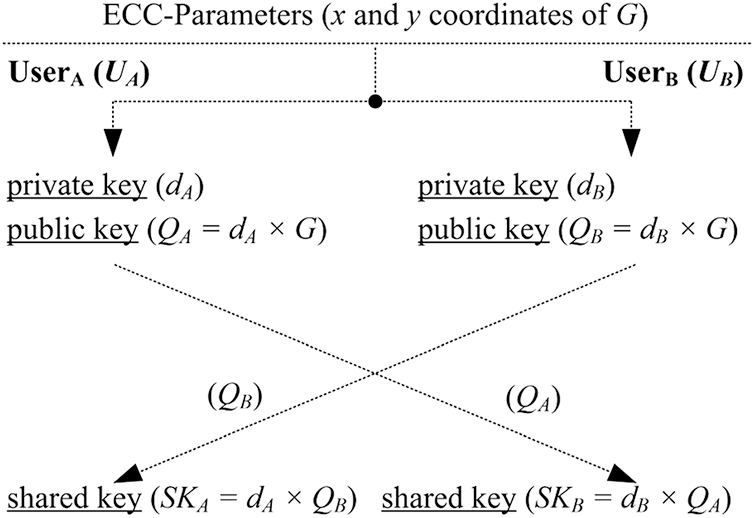
Figure 1: Layout of the ECDH protocol for key-agreement
As shown in Fig. 1, we have two distinct users, i.e.,
2.2 Elliptic-curve Point Multiplication
The PM operation is the computation of
In Eq. (1), G is the initial point on the curve, Q is the resultant point and d is a scalar multiplier (or a private key of the corresponding user). There are several algorithms in the literature such as Double and Add, Montgomery ladder, Lopez Dahab, and many more to operate the ECPM operation in ECC. A comprehensive comparison over various ECPM algorithms as hardware accelerators on FPGA and ASIC (application-specific integrated circuits) platforms is shown in [25]. Consequently, we have used the following Montgomery (Algorithm 1) algorithm because (inherently) it counters simple power analysis (SPA) attacks. It is important to note that we are implementing only the SPA attacks at the algorithmic level without realizing on a design level.
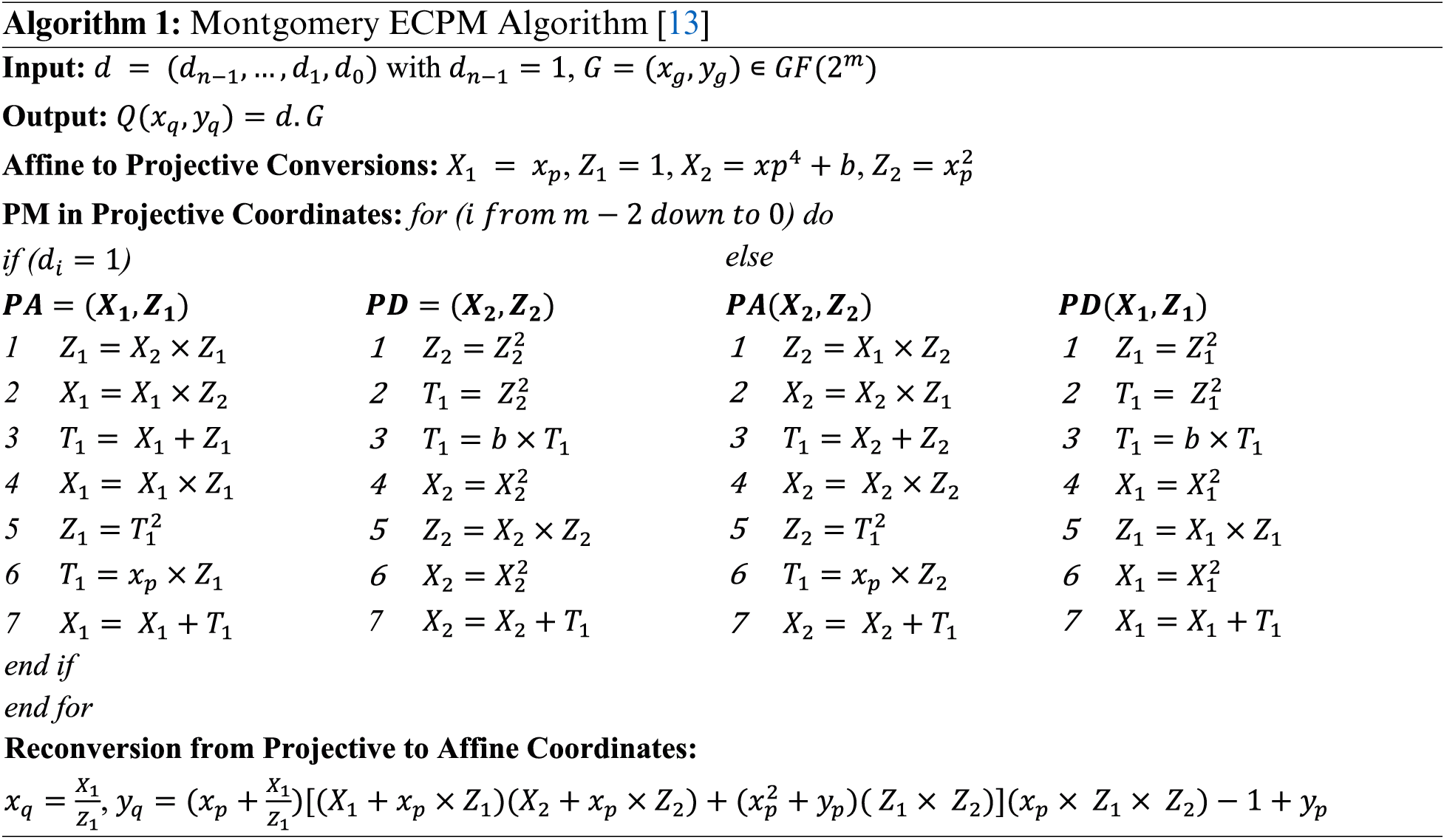
The inputs to Algorithm 1 are initial point G and a scalar multiplier d. A sequence
3 Proposed Key-Agreement Architecture
The proposed crypto processor architecture for ECDH is shown in Fig. 2. It consists of three blocks, i.e., (i) an ECDH controller, (ii) two routing multiplexers (
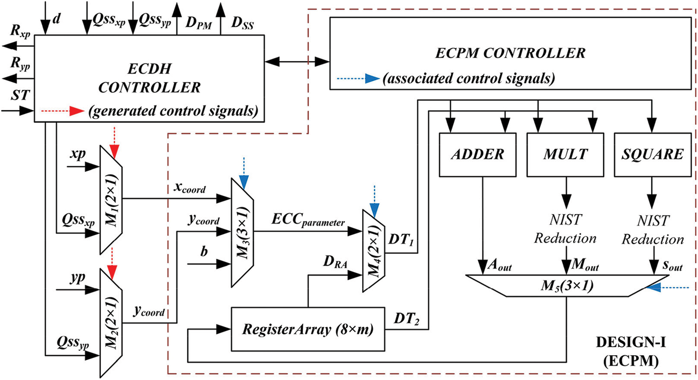
Figure 2: Proposed crypto processor architecture (DESIGN-II) for key-agreement of ECDH protocol
The ECDH controller is responsible for generating control signals for the routing multiplexers
The ECDH controller is implemented by adopting a finite state machine (FSM) model. It contains three states, i.e., IDLE, PKG and SKG. As the name implies, IDLE is the initial state of the crypto processor that determines none of the operations is under computation. The PKG shows that the crypto processor is processing a public key. Finally, the SKG means that the processor architecture is computing a shared key. A two-bit input signal “
3.2 Routing Multiplexers (
The purpose of
The ECPM unit consists of (i) an array of registers, (ii) three routing multiplexers, (iii) adder, squarer, multiplier, polynomial reduction & inversion units and (iv) an ECPM controller. The description of these units are given in the next subsequent sections:
The register array in the proposed crypto processor architecture is an
3.3.2 Three Routing Multiplexers (
The three routing multiplexers in the proposed architecture include
3.3.3 Adder, Squarer, Multiplier, Reduction and Inversion Units
The arithmetic operators, i.e., addition (ADDER), squaring (SQUARE) and multiplication (MULT), perform the PM operation of the ECPM unit. The implementation of a polynomial addition in
The efficiency of a polynomial multiplier specifies the performance of an ECC-based crypto processor architecture. Based on the available literature, there are four possibilities to implement a multiplier circuit. These possibilities are (i) bit-serial, (ii) digit-serial, (iii) bit-parallel and (iv) digit-parallel. Each aforementioned architectural choice has certain differences. When we consider only the computational cost in terms of clock cycles, the bit-serial multipliers require m cycles. On the other hand, one clock cycle is needed to implement the bit/digit parallel multiplication approaches. The digit-serial multipliers demand
The size of resultant polynomials generated after MULT and SQUARE units are
As shown in Algorithm 1, the reconversion from projective to affine requires two polynomial inversion computations. There are several inversion methods in the literature to perform the multiplicative inverse of the polynomial(s). Therefore, the Itoh Tsujii algorithm is extensively employed in the state-of-the-art because it needs multiplications and square operations for computation [13,17,18]. In this paper, we have (also) utilized the implementation resources of our employed MULT and SQUARE units to perform multiplicative inverse over polynomials using the Itoh Tsujii algorithm. Over
The FSM-based ECPM controller is responsible to perform the PM operation of Eq. (1). It generates the control signals to implement the Algorithm 1. The generated control signals for the routing multiplexers and register array are shown with blue color dotted lines in Fig. 2. The details of the ECPM controller is as follows:
• The proposed crypto processor will remain in state 0 (IDLE state).
• It starts the computation once it receives the
• Under different conditions, when the
3.4 Total Clock Cycles (TCC) Calculation for DESIGN-I and DESIGN-II
For the proposed DESIGN-I, Eq. (2) is used to calculate the total clock cycles. Similarly, the total cycles for DESIGN-II are calculated using Eq. (3).
In Eq. (2), 6 determines the clock cycles for the affine to projective conversion. The
As shown in Fig. 1, the ECDH scheme consists of dual PM computation (one for a public key generation and another for shared key). Therefore, Eq. (3) confirms that our DESIGN-II needs 163902 + 163902 (327804) clock cycles for one shared key generation between two distinct users (as we mentioned
4 Implementation Results and Comparisons
The details for the implementation results and comparison to state-of-the-art is given in Section 4.1 and Section 4.2, respectively.
Our DESIGN-I and DESIGN-II over
4.1.1 Area Utilization of Building Blocks of DESIGN-I and DESIGN-II
The area breakdown for building blocks in DESIGN-I and DESIGN-II are shown in Tab. 1. Column one provides the name of the building-blocks of our proposed design. From columns two to four, the area utilization is presented in terms of FPGA LUTs, Slices and FFs (flip-flops).
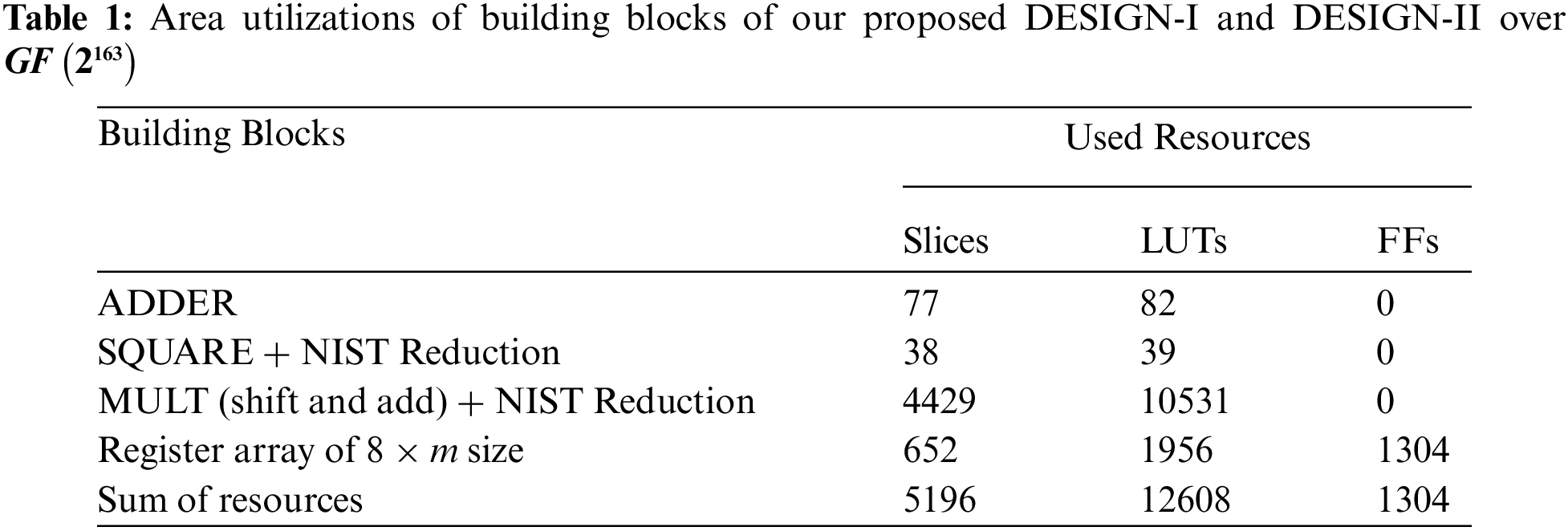
As shown in Tab. 1, the critical building blocks of DESIGN-I and DESIGN-II over Virtex-7 FPGA utilizes 77, 38, 4429 and 652 FPGA Slices for ADDER, SQUARE (including NIST Reduction), MULT (including NIST Reduction) and register array. Similarly, for identical building blocks, the LUTs utilization is 82, 39, 10531 and 1956. The sum of resources for building blocks is 5196 (Slices), 12608 (LUTs) and 1304 (FFs). Tab. 1 reveals that the MULT unit (even with simple shift and add architecture) utilizes more hardware resources as compared to other building blocks. Moreover, the implementation results show that the modular square operation being much simpler in the
Concerning the sum of resources of building blocks of our DESIGN-I and DESIGN-II, apart from the routing multiplexers, the reported Slices (5196) and LUTs (12608) values in Tab. 1 are still enough in large. Many area-constrained applications such as smart cards, IoT, automotive and several others demand lower hardware resources. In this regard, we have set design goals from balanced to area reduction in the Vivado IDE tool to minimize the hardware resources of our DESIGN-I and DESIGN-II implementations. Therefore, a description of the results is provided in the following section.
4.1.2 Implementation Results for DESIGN-I and DESIGN-II
The detailed implementation results of our proposed DESIGN-I and DESIGN-II are shown in Tab. 2. Column one provides the reference design. The area information in Slices, LUTS and FFs is given in columns two, three and four. Columns five and six provide the total clock cycles and operational clock frequency (in
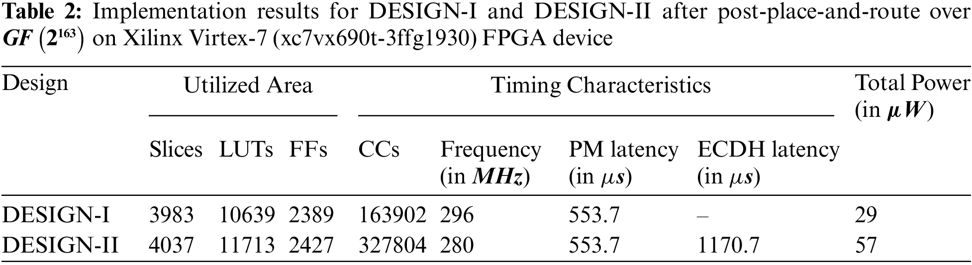
As shown in Tab. 2, the utilized hardware resources of DESIGN-I are 3983 (Slices), 10639 (LUTs) and 2389 (FFs). Similarly, the utilized resources of DESIGN-II are 4037 (Slices), 11713 (LUTs) and 2427 (FFs). The achieved clock frequency for DESIGN-I and DESIGN-II are 296
4.1.3 Area Comparison of DESIGN-I and DESIGN-II with the Sum of Slices and LUTs of Building Blocks
The total sum of Slices and LUTs of building blocks is 1.30 (ratio of 5196 with 3983) and 1.18 (ratio of 12608 with 10639) times higher than the Slices and LUTs of our DESIGN-I. Similarly, when the area resources of DESIGN-II are considered for comparison, the total sum of Slices and LUTs of building blocks is 1.28 (ratio of 5196 with 4037) and 1.07 (ratio of 12608 with 11713) times higher. This indicates that the use of different optimization strategies for synthesis of DESIGN-I and DESIGN-II results in lower resources. The reason is that we set the area optimization as synthesis goal in a Vivado IDE tool.
4.1.4 Comparison Between DESIGN-I and DESIGN-II
As far as the utilized area is concerned, DESIGN-I takes only the 3983, 10639 and 2389 Slices, LUTs and FFs. The reported FPGA area values in terms of Slices, LUTs and FFs for DESIGN-II are 4037, 11713 and 2427 that are comparatively 1.01 (ratio of 4037 with 3983), 1.10 (ratio of 11713 with 10639) and 1.01 (ratio of 2427 with 2389) times higher than our DESIGN-I. The reason for higher hardware resources in DESIGN-II is the use of two additional routing multiplexers (
4.2 Comparison with State-of-the-Art
The comparison with the most compatible state-of-the-art architectures, published in [13,16–19,22,24], is given in Tab. 3. The column one in Tab. 3 provides the reference design. The implemented PM algorithms and key-agreement protocols are presented in column two. The implementation device for logic synthesis is provided in column three. Column four presents the utilized FPGA slices. Finally, the last two columns (five and six) provide the clock frequency (in
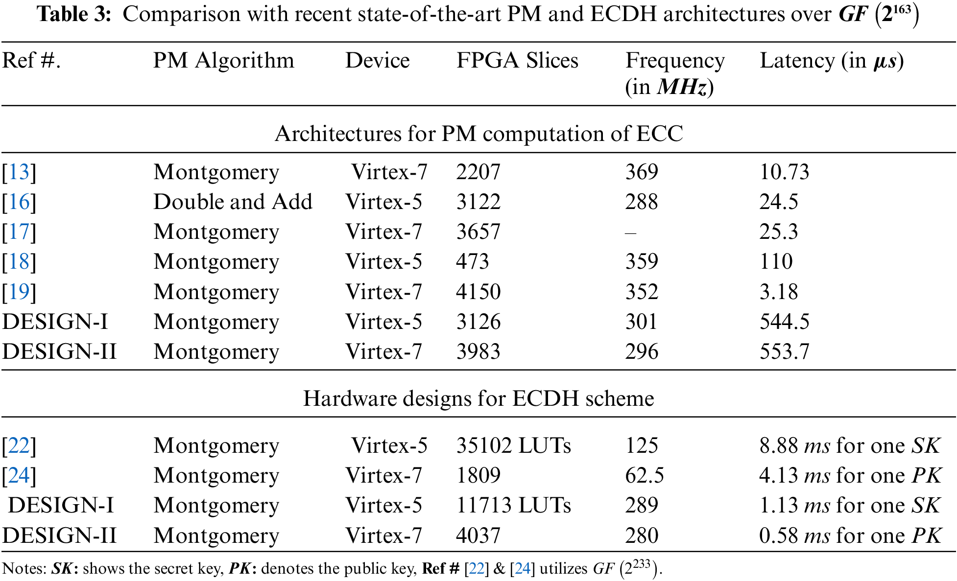
4.2.1 Comparison of our DESIGN-I with [16] and [19]
As compared to the dedicated PM architecture of [16] on Virtex-5 FPGA, our DESIGN-I utilizes 1.09 (3126 over 3122) times lower FPGA Slices. Moreover, in terms of clock frequency, our DESIGN-I is 1.04 (ratio of 301 over 288) times faster than [16]. On the other hand, the time required for one PM computation or public key generation in [16] is 22.2 (ratio of 544.5 over 24.5) times lower than our DESIGN-I. There is always a tradeoff between area and performance (latency) parameters. On Virtex-7 FPGA, a high-speed and latency optimized architecture of [19] for PM computation utilizes 4150 FPGA Slices which is comparatively 1.04 (ratio of 4150 over 3983) times higher than our DESIGN-I. Moreover, their architecture results in higher clock frequency (352
4.2.2 Design Tradeoffs Between [13,17,18] and our DESIGN-I
As shown in Tab. 3, the dedicated PM architectures (reported in [13,17,18]) over Virtex-5 and Virtex-7 FPGA devices show that there is always a tradeoff between several design parameters when implementing the cryptographic algorithms as a hardware accelerator. In the text that follows, a tradeoff by providing the comparison of dedicated PM designs (published in [13,17,18]) with our notion of a flexible crypto processor (DESIGN-I) is described. As reported earlier in this paper, flexibility determines the selection of ECC parameters according to the user’s needs (readers can turn to multiplexer
On Virtex-7 FPGA, a 2-stage pipelined PM architecture of [13] utilizes 1.80 (ratio of 3983 over 2207) times lower Slices as compared to our DESIGN-I. The reason for the utilization of lower hardware resources is the use of only one multiplier architecture for both square and polynomial multiplication computations. The square operations are computed by providing similar inputs to the multiplier unit. Additionally, the use of a singular NIST reduction unit also leads to a decrease in hardware resources. Comparatively, we are using a separate MULT and SQUARE unit to operate polynomial multiplications and squaring operations, respectively. In addition, we have two NIST reduction units connected one after each MULT and SQUARE unit in our designs. These architectural differences result in an increase in hardware resources in our work. Due to pipelining in [13], the achieved clock frequency is a bit higher than our crypto processor design. Furthermore, the time to operate one PM computation is lower than our DESIGN-I. In [17], 3657 FPGA Slices is used on Virtex-7 FPGA for the PM computation over
As compared to the PM architecture of [18] on Virtex-5 FPGA, our DESIGN-I consumes 6.6 (ratio of 3126 to 473) times higher FPGA Slices. The reason is the employment of two NIST reduction units, one after in each SQUARE and MULT unit in our architecture. Moreover, a segmented digit serial multiplier architecture is used in [18] while in our design, a shift and add multiplication method is used for polynomial multiplication. Similar to the area (FPGA slices), the dedicated PM architecture of [18] achieves higher clock frequency and requires lower computational time as compared to our DESIGN-I. One of the reasons for this is to consider flexibility when selecting different curve parameters as inputs to our DESIGN-I using routing multiplexers
Remarks: We are not asserting that our DESIGN-I outperforms (in terms of hardware area) in all state-of-the-art PM implementations. There is always a tradeoff when considering several design parameters concurrently for optimizations. Therefore, based on the comparisons presented above, we have noted that the hardware accelerators of ECC for only optimized for PM computation can result in little unfair measurements when scaling the same PM architecture to any ECC protocol (such as ECDH in this work). Therefore, a hardware architecture with the considerations of all four layers could be more beneficial.
4.2.3 Comparison of our DESIGN-II (ECDH) with [22] and [24]
The accelerator architectures of [22,24] for ECDH scheme are presented over
This paper has presented a key-agreement architecture for the ECDH scheme over
Acknowledgement: We extend our gratitude to the Estonian Aviation Academy, Tartu, Estonia for supporting and funding this research work.
Funding Statement: We acknowledge the support of Deanship of Scientific Research at King Khalid University for funding this work under grant number R.G.P.1/399/42.
Conflicts of Interest: The authors declare that they have no conflicts of interest to report regarding the present study.
1. K. Tamilarasi and A. Jawahar, “Medical data security for healthcare applications using hybrid lightweight encryption and swarm optimization algorithm,” Wireless Personal Communication, vol. 114, no. 3, pp. 1865–1886, 2020. [Google Scholar]
2. S. Tangade, S. S. Manvi and P. Lorenz, “Trust management scheme based on hybrid cryptography for secure communications in vanets,” IEEE Transactions on Vehicular Technology, vol. 69, no. 5, pp. 5232–5243, 2020. [Google Scholar]
3. P. S. Murvay and B. Groza, “Efficient physical layer key agreement for flexray networks,” IEEE Transactions on Vehicular Technology, vol. 69, no. 9, pp. 9767–9780, 2020. [Google Scholar]
4. H. Yang, Q. Zhou, M. Yao, R. Lu, H. Li et al., “A practical and compatible cryptographic solution to ADS-B security,” IEEE Internet of Things Journal, vol. 6, no. 2, pp. 3322–3334, 2019. [Google Scholar]
5. G. Andrei, T. Polishchuk and M. Wernberg. “Controller–pilot data link communication security,” Sensors, vol. 18, no. 5, pp. 1636, 2018. [Google Scholar]
6. Y. Eslami, A. Sheikholeslami, P. G. Gulak, S. Masui and K. Mukaida, “An area-efficient universal cryptography processor for smart cards,” IEEE Transactions on Very Large Scale Integration (VLSI) Systems, vol. 14, no. 1, pp. 43–56, 2006. [Google Scholar]
7. R. A. Nelson, “Authentication Techniques for Smart Cards,” United States, 1994. [Online]. Available: https://www.osti.gov/servlets/purl/10141490. [Google Scholar]
8. R. Vinoth, L. J. Deborah, P. Vijayakumar and N. Kumar, “Secure multifactor authenticated key agreement scheme for industrial IoT,” IEEE Internet of Things Journal, vol. 8, no. 5, pp. 3801–3811, 2021. [Google Scholar]
9. J. Srinivas, A. K. Das, M. Wazid and N. Kumar, “Anonymous lightweight chaotic map-based authenticated key agreement protocol for industrial internet of things,” IEEE Transactions on Dependable and Secure Computing, vol. 17, no. 6, pp. 1133–1146, 2020. [Google Scholar]
10. K. Sahu, S. Sharma and D. Puthal, “Lightweight multi-party authentication and key agreement protocol in IoT-based e-healthcare service,” ACM Transactions on Multimedia Computing, Communications, and Applications, vol. 17, no. 2s, pp. 1–20. 2021. [Google Scholar]
11. S. M. Z. Khan, Y. L. Moullec and M. M. Alam, “An NB-IoT based edge-of-things framework for energy-efficient image transfer,” Sensors, vol. 21, no. 17, pp. 5929, 2021. [Google Scholar]
12. S. M. Z. Khan, M. M. Alam, Y. L. Moullec, A. Kuusik, S. Pärand et al., “An empirical modeling for the baseline energy consumption of an NB-IoT radio transceiver,” IEEE Internet of Things Journal, vol. 8, no. 19, pp. 14756–14772, 2021. [Google Scholar]
13. M. Imran, M. Rashid, A. R. Jafri and M. Kashif, “Throughput/area optimised pipelined architecture for elliptic curve crypto processor,” IET Computers & Digital Techniques, vol. 13, no. 5, pp. 361–368, 2019. [Google Scholar]
14. M. M. Islam, M. S. Hossain, M. Shahjalal, M. K. Hasan and Y. M. Jang, “Area-time efficient hardware implementation of modular multiplication for elliptic curve cryptography,” IEEE Access, vol. 8, pp. 73898–73906, 2020. [Google Scholar]
15. D. Hankerson, A. J. Menezes and S. Vanstone, “Guide to Elliptic Curve Cryptography,” Henderson, NV, USA: Springer, pp. 1–311, 2004. [Online]. Available: https://link.springer.com/book/10.1007/b97644. [Google Scholar]
16. B. Rashidi, “Low-cost and fast hardware implementations of point multiplication on binary edwards curves,” in Electrical Engineering (ICEEIranian Conf. on, Mashhad, Iran, pp. 17–22, 2018. [Google Scholar]
17. M. Imran, M. Rashid and I. Shafi, “Lopez dahab based elliptic crypto processor (ECP) over GF(2163) for low-area applications on FPGA,” in 2018 Int. Conf. on Engineering and Emerging Technologies (ICEET), Lahore, Pakistan, pp. 1–6, 2018. [Google Scholar]
18. Z. U. A. Khan and M. Benaissa, “Low area ECC implementation on FPGA,” in 2013 IEEE 20th Int. Conf. on Electronics, Circuits, and Systems (ICECS), Abu Dhabi, United Arab Emirates, pp. 581–584, 2013. [Google Scholar]
19. Z. U. A. Khan and M. Benaissa, “High-speed and low-latency ECC processor implementation over
20. J. Li, W. Wang, J. Zhang, Y. Luo and S. Ren, “Innovative dual-binary-field architecture for point multiplication of elliptic curve cryptography,” IEEE Access, vol. 9, pp. 12405–12419, 2021. [Google Scholar]
21. S. Liu, L. Ju, X. Cai, Z. Jia and Z. Zhang, “High performance FPGA implementation of elliptic curve cryptography over binary fields,” in 2014 IEEE 13th Int. Conf. on Trust, Security and Privacy in Computing and Communications, Beijing, China, pp. 148–155, 2014. [Google Scholar]
22. A. P. Fournaris, I. Zafeirakis, C. Koulamas, N. Sklavos and O. Koufopavlou, “Designing efficient elliptic curve diffie-hellman accelerators for embedded systems,” in 2015 IEEE Int. Symp. on Circuits and Systems (ISCAS), Lisbon, Portugal, pp. 2025–2028, 2015. [Google Scholar]
23. D. Ionita and E. Simion, “FPGA offloading for diffie-hellman key exchange using elliptic curves,” Cryptology ePrint Archive, Report 2021/065, 2021. [Online]. Available: https://ia.cr/2021/065. [Google Scholar]
24. M. Morales-Sandoval, L. A. R. Flores, R. Cumplido, J. J. Garcia-Hernandez, C. Feregrino et al., “A compact FPGA-based accelerator for curve-based cryptography in wireless sensor networks,” Journal of Sensors, vol. 2021, pp. 13, 2021. [Google Scholar]
25. M. Rashid, M. Imran, A. R. Jafri and T. F. Al-Somani, “Flexible architectures for cryptographic algorithms: A systematic literature review,” Journal of Circuits Systems and Computers, vol. 28, no. 3, pp. 35, 2019. [Google Scholar]
26. NIST. “Recommended Elliptic Curves for Federal Government use,” 1999. [Online]. Available: https://csrc.nist.gov/csrc/media/publications/fips/186/2/archive/2000-01-27/documents/fips186-2.pdf. [Google Scholar]
27. P. Zode, R. B. Deshmukh and A. Samad, “Fast architecture of modular inversion using Itoh-Tsujii algorithm,” in VLSI Design and Test, Singapore: Springer, pp. 48–55, 2017. [Online]. Available: https://www.springerprofessional.de/fast-architecture-of-modular-inversion-using-itoh-tsujii-algorit/15326436. [Google Scholar]
28. XILINX, “7 Series Product Selection Guide,” [Online]. Available: https://www.xilinx.com/products/silicon-devices/fpga/virtex-7.html. [Google Scholar]
 | This work is licensed under a Creative Commons Attribution 4.0 International License, which permits unrestricted use, distribution, and reproduction in any medium, provided the original work is properly cited. |