DOI:10.32604/cmc.2022.030193
| Computers, Materials & Continua DOI:10.32604/cmc.2022.030193 | |
| Article |
Design of a Novel THz Modulator for B5G Communication
Department of Electrical Engineering, Faculty of Engineering, The Hashemite University, Zarqa, 13133, Jordan
*Corresponding Author: Omar A. Saraereh. Email: eloas2@hu.edu.jo
Received: 21 March 2022; Accepted: 21 April 2022
Abstract: Wireless data traffic has expanded at a rate that reminds us of Moore’s prediction for integrated circuits in recent years, necessitating ongoing attempts to supply wireless systems with ever-larger data rates in the near future, despite the under-deployment of 5G networks. Terahertz (THz) communication has been considered a viable response to communication blackout due to the rapid development of THz technology and sensors. THz communication has a high frequency, which allows for better penetration. It is a fast expanding and evolving industry, driven by an increase in wireless traffic volume and data transfer speeds. A THz modulator based on a hybrid metasurface was devised and built in this work. The device’s modulation capabilities were modelled and proved experimentally. The electrolyte is an ion-gel medium implanted between graphene and metasurface, and the active material is graphene. On the metasurface, the interaction between the THz wave and graphene is improved. Additionally, an external bias voltage was employed to actively regulate the THz waves by tuning the electrical conductivity of graphene. The results show that with a minimal bias voltage, the device can achieve a modulation depth of up to 73% at the resonant frequency. Furthermore, during the modulation process, the resonance frequency remains almost constant. As a result, the proposed gadget offers a unique tool for substantial THz amplitude modulation at low voltages.
Keywords: Terahertz communication; modulator; metasurface; graphene
Terahertz waves refer to electromagnetic waves with a frequency range between 0.1 and 10 THz, which are located between infrared and millimeter waves in the electromagnetic spectrum. The reason why terahertz waves can attract the attention of researchers is that their special spectral position and spectral characteristics make them useful in the fields of national economy and national defense construction such as material structure exploration and identification, security inspection, biomedical imaging, radar and ultra-wideband communication It has broad application prospects [1]. However, due to the high-efficiency emission sources operating in the terahertz band in the past, detectors and functional devices are few or expensive, the terahertz technology is still far from practical application. Now, great progress has been made in the research of terahertz emission sources and detectors, and various terahertz technologies have been gradually proposed, including photoconductive antennas, optical rectification, Semiconductor surface emission, air plasma four-wave mixing and metal thin film spin current and other technologies [2,3]. In contrast, functional devices for controlling terahertz waves are still lacking. Therefore, the development of compact, high-performance, high-design freedom, and high-efficiency functional devices in the terahertz band is an urgent problem to be solved, which is of great significance for promoting the development of terahertz science and technology. The emergence of metamaterials and metasurfaces provides an effective means to solve this problem.
Metamaterials refer to novel materials composed of subwavelength artificial microstructures, which can efficiently and freely manipulate the propagation of electromagnetic waves. Due to the randomness of the design of the microstructure and arrangement of metamaterials, metamaterials can achieve many functions that cannot be achieved by natural materials, such as negative refractive index, stealth, super imaging, etc., refreshing people’s understanding of electromagnetic wave manipulation [4]. These metamaterials are all three-dimensional structures, which are difficult to process and suffer from high losses in practical applications. In contrast, research on metasurfaces has attracted more attention. Metasurface refers to a two-dimensional metamaterial composed of subwavelength artificial microstructures arranged in an array at the interface. It can not only control the transmission of electromagnetic waves, but also control other parameters of electromagnetic waves, such as amplitude, phase, polarization, frequency, and wavefront, etc. [5]. Compared with three-dimensional metamaterials, the processing of metasurfaces is simpler, and because the length of the interaction with electromagnetic waves is drastically reduced and the loss is lower, it is more suitable for the fabrication of devices. Like metamaterials, research on metasurfaces has also arisen in the microwave and infrared bands, and has now almost extended to the entire electromagnetic spectrum [6]. For the terahertz band where functional devices are lacking, the emergence of metasurfaces undoubtedly opens up a new path for them. At present, in the terahertz band, many functional devices based on metasurfaces have been reported, such as filters [7,8], absorbers [9], modulators [10], polarization controllers [11], wavefront control [12], and so on. However, it can be noticed that most of these devices are passive, and it is expected that more active and controllable terahertz functional devices can be realized on this basis. For this reason, the emerging two-dimensional material, graphene, has attracted extensive attention of researchers.
As a typical representative of two-dimensional materials, graphene has been widely studied in many fields such as physics, chemistry, energy and materials due to its unique mechanical, thermal and electromagnetic properties [13]. Graphene is a two-dimensional planar material composed of a single layer of carbon atoms arranged in a honeycomb shape, and its thickness is about 0.3 nm. The ideal graphene has a tapered band structure with no bandgap and high carrier mobility at room temperature [14,15], which provides the possibility for the rapid operation of optoelectronic devices. Different from other materials, the electrical conductivity of graphene is jointly determined by interband transitions and intraband transitions [16]. In the visible light band, the photoconductivity of graphene is almost unchanged, and the absorption rate of visible light is only 2.3%, which is an ideal transparent electrode material [17]. In the terahertz band, the conductivity of graphene depends on the in-band transition. By moving the position of the Fermi level by voltage, chemical doping, etc., the size of its conductivity can be changed, and then its interaction with terahertz waves can be changed. strength. Based on the remarkable tunability of graphene’s electrical conductivity in the terahertz band, researchers have proposed many terahertz master devices using graphene as an active material. Example: Transferring graphene onto silicon-based silicon dioxide creates a terahertz amplitude modulator can achieve 15% modulation of terahertz wave under 50 V external bias voltage [18]. By etching graphene into periodic rectangular or L-shaped shapes, ultrathin, broadband, and tunable polarization-controlling devices operating at terahertz frequencies have been realized [19]. In addition, graphene-based terahertz absorbers have also been proposed [20−22].
As an active controllable material, graphene has shown great application prospects in the development of terahertz functional devices, but its thickness (nanoscale) limits the strength of its interaction with terahertz waves. Within a given range of graphene conductivity fluctuations, the stronger the plane electric field where graphene is located, the more sensitive the terahertz wave transmission is to the graphene conductivity. By combining graphene with a metasurface, the strength of the interaction between graphene and terahertz waves can be enhanced to a certain extent, that is, its ability to control terahertz waves is enhanced, thereby promoting the development of terahertz master devices. Reference [23] directly transferred graphene to a silicon substrate, and then combined it with a metasurface to achieve 60% modulation of terahertz waves at a relatively small voltage by using a method of optoelectronic hybrid modulation. Reference [24] designed an ultrathin broadband terahertz metamaterial absorber based on patterned graphene, which achieved more than 80% absorption of terahertz waves, and the absorption bandwidth reached 1.422 THz. Reference [25] proposed an electronically controlled terahertz polarization device composed of a chiral metasurface and graphene, which realized the polarization of right-handed circularly polarized light without changing the left-handed circularly polarized light. Reference [26] combined metal metasurfaces and graphene, and proposed a master terahertz metalens, which achieved a focal length from 10.46 to 12.24 mm under a bias voltage of 0~2 V.
The ionic gels formed by mixing polymers with ionic liquids have good electrical conductivity and large mechanical strength, and have received extensive attention in the study of electrically controlled graphene Fermi levels. In this paper, a terahertz amplitude modulation device is proposed based on artificial iongel and graphene metasurface. Unlike previously proposed terahertz modulation devices, this study embeds ion gels on metasurfaces and between graphenes, by applying an external bias, a nanometer-thick electric double layer is formed at the interface between graphene and ion gel, similar to a supercapacitor, which can greatly adjust the Fermi level of graphene, so a small voltage can significantly change the electrical conductivity of graphene to achieve the purpose of controlling terahertz waves. The experimental measurements show that the device can achieve a modulation depth of 64% under an external bias voltage of 3.0 V while keeping the resonant frequency almost unchanged. On this basis, the modulation depth can be further increased to 73% by increasing the number of graphene layers interacting with the metal structure to two layers. In addition, numerical simulations are carried out for devices composed of metal structures with different feature sizes, and the simulation results show that by adjusting the size of the metal structures, large-scale modulation of terahertz waves at different frequencies can be achieved. This low-voltage, large modulation depth THz AM device is of great significance to promote the development and practical application of THz technology.
2 System Modelling and Experimentations
Fig. 1a is a schematic diagram of the structure of the terahertz amplitude modulation device designed, which has a single layer of graphene, an ion gel and a metal metasurface in sequence on a quartz substrate. Among them, the metasurface is an “I”-shaped aperture structure, as shown in Fig. 1b. The structure size parameters are as follows:
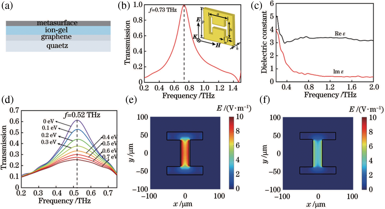
Figure 1: Proposed system evaluation. (a) sample structure, (b) spectrum and metasurface, (c)
where,
where
In addition, the modulation effects of the modulation devices composed of metasurfaces with different feature sizes (similar to the structure shown in Fig. 1b, the only difference is the value of the parameter a, where a is 100 and 140 μm, respectively) are evaluated. The simulation results are shown in Figs. 2a–2d. It can be seen that by changing the feature size of the metal structure, the operating frequency of the device can be adjusted in a wide range on the premise of maintaining the modulation depth. The resonant frequencies of these structures are located at 0.48 and 0.58 THz, respectively. Further, the electric field distributions of the two structures at their resonant frequencies are simulated, and their electric field distributions at 0 and 0.5 eV are shown in Figs. 2b–2c and Figs. 2e–2f, respectively. It can be seen that, as the Fermi level of graphene increases, the strength of the local electric field decreases continuously. It can be seen that by adjusting the parameters of the metasurface geometry, active modulation of the amplitude at different terahertz frequencies can be achieved. In order to further explain the modulation mechanism of the device, the electric field distribution on the surface of the metal structure at a frequency of 0.52 THz was simulated. The results when the Fermi level is 0 and 0.5 eV are shown in Figs. 1e–1f, respectively. It can be seen that the electric field is always localized at the center of the “I”-shaped pore structure, and as the Fermi level of graphene increases, the strength of the local electric field is significantly weakened, because the increase of the Fermi level will lead to graphite. The conductivity of the alkene layer increases, thereby enhancing the short-circuit effect on the resonance of the metal structure, weakening the strength of the local electric field, and thus reducing the transmittance of the device at the peak.
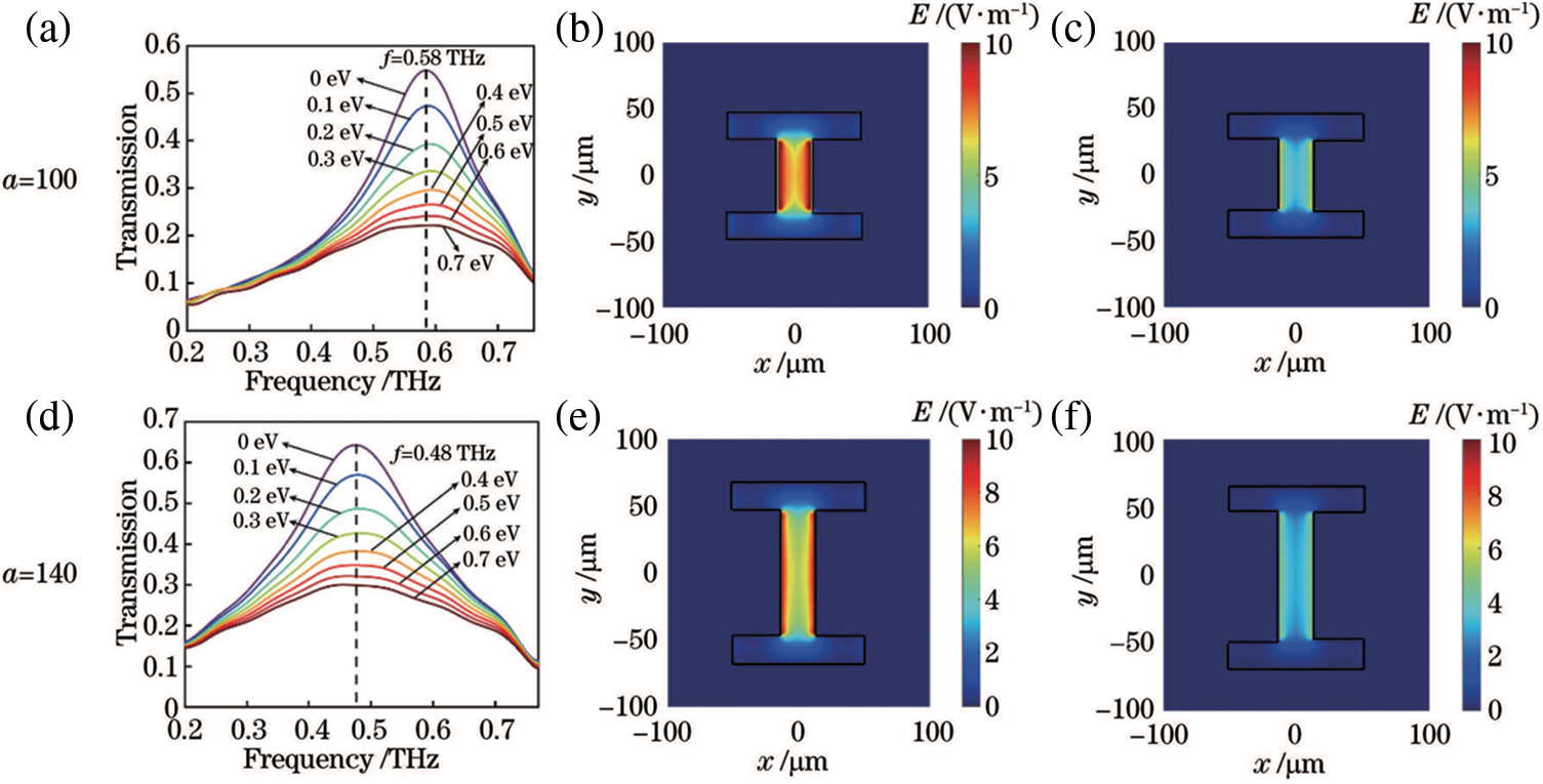
Figure 2: Simulation evaluation of various parameters. (a), (d) transmission spectra, (b), (e) field distribution for 0 eV, (c) (f) field distribution for 0.5 eV
The modulation effect of the device will be verified by experiments in the following. The structure of the experimental sample is shown in Fig. 3a, and its processing flow is as follows. First, an “I”-shaped aperture metasurface made of nickel was fabricated by traditional photolithography and chemical methods. Next, a single-layer graphene with a size of 1 cm × 1 cm was transferred to the surface of the quartz substrate by the commonly used wet transfer method [28−30], and a strip electrode in contact with the graphene was fabricated by silver glue, in which the graphite used in the experiment was used. The graphene was grown by chemical vapor deposition (CVD) method. Then, the ionogel spin-coating solution was uniformly spin-coated on the graphene surface using a spinner (at a speed of 3000 r/min), and then baked at 70°C for 24 h. The residual acetone solvent in the gel was removed, so far, a uniform ion gel film was formed on the graphene surface. After that, another strip electrode was fabricated on the upper surface of the ion gel using silver glue, and the fabricated metal structure was pasted on the ion gel, finally forming a composite structure. The spin coating solution was obtained by mixing polymer P (VDF-HFP), ionic liquid ([EMIM][TFSI]) and acetone in a mass ratio of 1:4:7 and stirring at 50°C for 2 h.
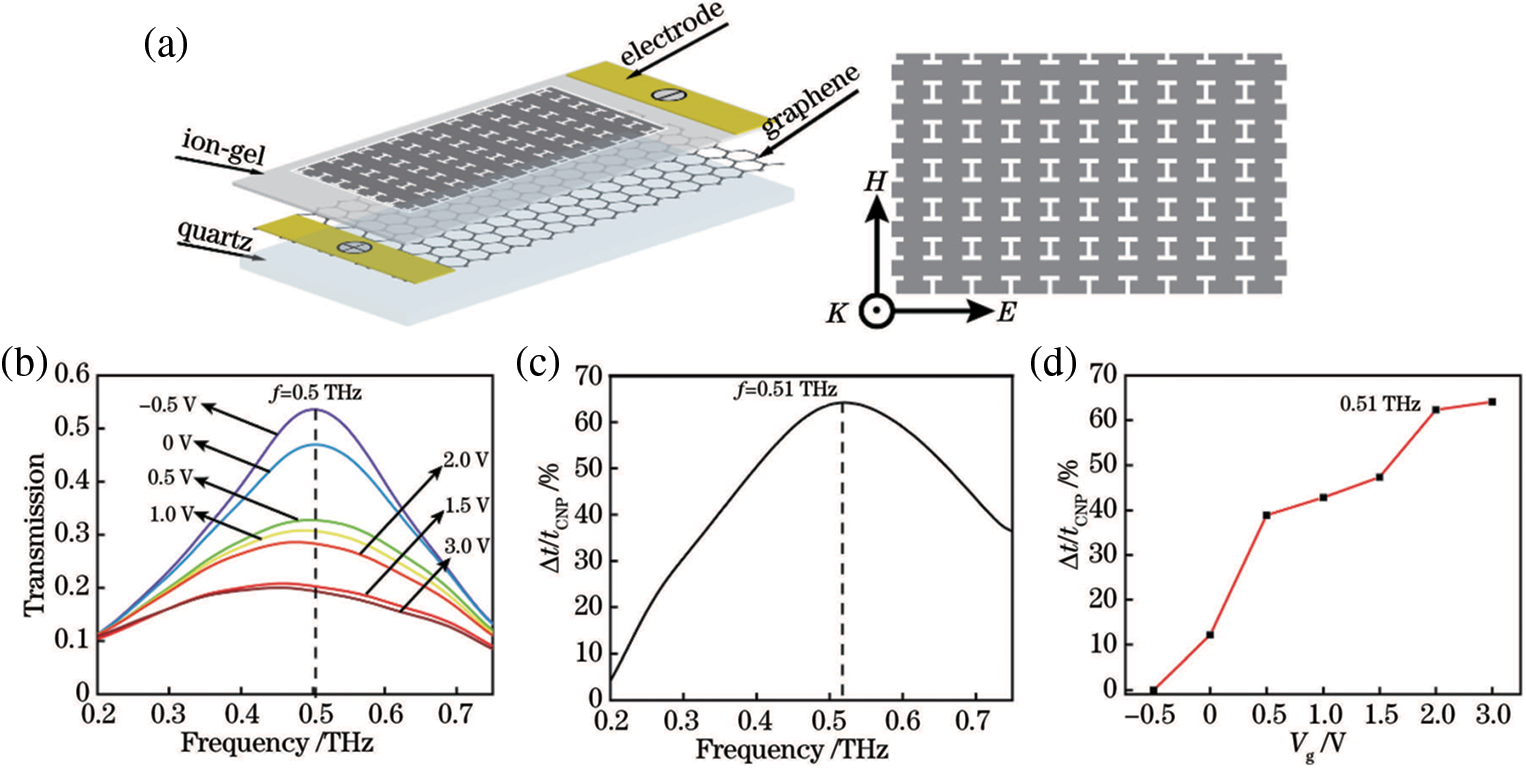
Figure 3: Proposed system. (a) architecture, (b) transmission spectra, (c) depth of modulation against frequency, (d) depth of modulation against external bias voltage
The Fermi level of graphene is closely related to the applied bias, that is,
In order to gain an in-depth understanding of the modulation mechanism, our group designed and fabricated a terahertz amplitude modulation device composed only of single-layer graphene and ion gel, the schematic diagram of which is shown in Fig. 4a. The device is the same as the sample with metal structure, the positive and negative electrodes are added on the surface of graphene and ion gel, respectively. Similarly, the transmittance of the sample was measured by the terahertz time-domain spectroscopy system. Fig. 4b is the transmittance spectrum of the sample under different applied bias voltages, and Fig. 4c is the sample under 3.0 V applied bias voltage. Compared with the THz AM device based on the metasurface/ion gel/graphene composite structure, the modulation depth of the THz AM device based on the graphene/ion gel structure is significantly reduced.

Figure 4: Illustrations of the proposed THz device. (a) structure, (b) transmission spectra, (c) depth of modulation against frequency
Based on the above experimental results, it can be seen that the terahertz amplitude modulation device based on the artificial metasurface/ion gel/graphene composite structure can achieve a large modulation of the terahertz wave at a relatively small voltage, and the modulation effect is a metallic structure. Under the applied bias voltage, positive and negative ions gather at the interface of ion gel and graphene, forming an electric double layer (EDL) structure with nanometer thickness, and the applied bias voltage is large. Part of it falls in the electric double layer, forming a very strong electric field, so only a small voltage is needed to achieve a large modulation of the Fermi level [33], and then the effect of modulation of terahertz waves can be achieved. In addition, after adding the metal resonant structure, since the thickness of the ion gel is only a few micrometers, the graphene is still in the electric field localized by the metal structure [34], which enhances the interaction between the metal structure and graphene, thus further improving the modulation depth of the device.
4 Two-Layer Graphene-Based THz Device
In order to further increase the modulation depth of the device, on the basis of the above modulation device, our group designed and fabricated an amplitude modulation device composed of two single-layer graphenes, the structure of which is shown in Fig. 5a. In this structure, two single-layer graphene layers are placed on both sides of the metal resonant structure, and the two graphene layers are used as the positive and negative electrodes of the device, respectively. In the presence of an external bias voltage, an electric double layer is formed at the upper and lower graphene and ion gel interfaces, resulting in the rise of the Fermi level of one layer of graphene and the decrease of the Fermi level of the other layer of graphene, which leads to this phenomenon. The conductivity of the two-layer graphene increases with the increase of the voltage at the same time, and the two-layer graphene has a short-circuit effect on the resonance of the metal structure, so this structure can further increase the modulation of the terahertz wave. Similarly, the transmission spectra of the samples under different bias voltages were measured by the terahertz time-domain spectroscopy system, and the results are shown in Fig. 5b. It should be noted that the reference at this time is the transmission spectrum of two non-contact quartz plates. It can be seen that the resonant frequency of this device still appears at 0.51 THz, and the transmittances under 0 V and 3.0 V bias voltages are 0.60 and 0.16, respectively. In order to visually see the modulation performance of the device, the modulation depth at different frequencies is calculated (the modulation depth at this time is defined) as:

Figure 5: Proposed THz bilayer graphene device. (a) architecture, (b) spectra vs f, (c) depth of modulation against frequency, (d) depth of modulation against bias voltage
The modulation speed of the sample shown in Fig. 5a is measured, and the measurement device is shown in Fig. 6a. Among them, VDI is used to generate continuous terahertz waves with a center frequency of 0.51 THz, and an off-axis parabolic mirror (OAPM) collimates and focuses the continuous terahertz waves generated by VDI on the sample. After the Gaolai cell is placed on the sample, it is used to detect the terahertz power transmitted through the sample;

Figure 6: Experimental evaluation of the proposed THz device. (a) setup for measurement, (b) result
The lock-in amplifier is connected to the Golay box to extract the variation of terahertz optical power. During the measurement, a square wave modulation voltage of 0~3V was applied to both ends of the sample electrode. Fig. 6b shows the change trend of the normalized optical power transmitted through the sample under the action of the square wave voltage of different frequencies. As the frequency of the voltage applied across the sample increases from 0 to 30 Hz, the optical power transmitted through the sample decreases continuously. Taking the point at 3 dB as the cut-off frequency of the device, it can be estimated that the modulation speed of the device is about 4.5 Hz, which can meet the needs of some practical applications.
This research article proposes a terahertz amplitude modulation device based on an artificial metasurface/ion gel/graphene composite structure. In this device, the ability of the metasurface to localize the surface electric field enhances the strength of the interaction between terahertz waves and graphene, and under an applied bias, the graphene-iongel interface forms an electric double layer with nanometer thickness, similar to For supercapacitors, the electrical conductivity of graphene can be greatly adjusted, on the one hand, its interaction with terahertz waves is changed, and on the other hand, the resonant ability of the metasurface is changed, and finally the effect of modulating the amplitude of terahertz waves is achieved. The design using double-layer graphene can achieve better modulation effect than single-layer graphene, which can achieve a modulation depth of 73% at the resonant frequency under an applied bias of 3.0 V, and the resonant frequency during the modulation process is 73% remained almost unchanged. In addition, the use of metasurfaces with different geometries or feature sizes can realize modulation functions at different frequencies. The active terahertz amplitude modulation device based on the metasurface/ion gel/graphene composite structure proposed by this research group can achieve a relatively large amplitude terahertz modulation under a small applied bias voltage, which is a promising candidate for emerging terahertz functional devices. development provides an effective way.
Acknowledgement: The author would like to thanks the editors and reviewers for their review and recommendations.
Funding Statement: The author received no specific funding for this study.
Conflicts of Interest: The author declare that he has no conflicts of interest to report regarding the present study.
1. A. Ashyap, S. Alamri, S. Dahlan, Z. Abidin, M. Abbasi et al., “Triple-band metamaterial inspired antenna for future terahertz (THz) applications,” Computers Materials & Continua, vol. 72, no. 1, pp. 1071–1087, 2022. [Google Scholar]
2. K. Kato, “Photonics-assisted terahertz-wave beam steering and its application in secured wireless communication,” Photonics Journal, vol. 9, no. 1, pp. 1–17, 2022. [Google Scholar]
3. T. Seifert, S. Jaiswal and U. Martens, “Efficient metallic spintronic emitters of ultrabroadband terahertz radiation,” Nature Photonics, vol. 10, no. 7, pp. 483–488, 2016. [Google Scholar]
4. R. Xu and Y. Lin, “Actively MEMS-based tunable metamaterials for advanced and emerging applications,” Electronics Journal, vol. 11, no. 2, pp. 1–18, 2022. [Google Scholar]
5. N. Yu and F. Capasso, “Flat optics with designer metasurfaces,” Nature Materials, vol. 13, no. 2, pp. 139–150, 2014. [Google Scholar]
6. S. Glybovski, S. Tretyakov and P. Belov, “Metasurfaces: From microwaves to visible,” Physics Reports Journal, vol. 634, no. 3, pp. 1–72, 2016. [Google Scholar]
7. Q. Li, X. Zhang and W. Cao, “An approach for mechanically tunable, dynamic terahertz bandstop filters,” Applied Physics A Journal, vol. 107, no. 2, pp. 285–291, 2012. [Google Scholar]
8. J. Yang and Y. Lin, “Design of tunable terahertz metamaterial sensor with single-and dual-resonance characteristics,” Nanomaterials Journal, vol. 11, no. 9, pp. 1–18, 2021. [Google Scholar]
9. X. Zhang, N. Xu and K. Qu, “Electromagnetically induced absorption in a three-resonator metasurface system,” Scientific Reports, vol. 5, no. 1, pp. 10737–10748, 2015. [Google Scholar]
10. Q. Li, Z. Tian and X. Zhang, “Active graphene-silicon hybrid diode for terahertz waves,” Nature Communications, vol. 6, no. 1, pp. 7082–7093, 2015. [Google Scholar]
11. L. Cong, N. Xu and W. Zhang, “Polarization control in terahertz metasurfaces with the lowest order rotational symmetry,” Advanced Optical Materials, vol. 3, no. 9, pp. 1176–1183, 2015. [Google Scholar]
12. H. Zhang, M. Kang and X. Zhang, “Coherent control of optical spin-to-orbital angular momentum conversion in metasurface,” Advanced Materials, vol. 29, no. 6, pp. 160–175, 2017. [Google Scholar]
13. D. Nurrohman and N. Chiu, “A review of graphene-based surface plasmon resonance and surface-enhanced raman scattering biosensors: Current status and future prospects,” Nanomaterials Journal, vol. 11, no. 1, pp. 1–19, 2021. [Google Scholar]
14. T. Kampfrath, L. Perfetti and F. Schapper, “Strongly coupled optical phonons in the ultrafast dynamics of the electronic energy and current relaxation in graphite,” Physical Review Letters, vol. 95, no. 18, pp. 187–199, 2005. [Google Scholar]
15. Z. Li, E. Henriksen and Z. Jiang, “Dirac charge dynamics in graphene by infrared spectroscopy,” Nature Physics, vol. 4, no. 7, pp. 532–535, 2008. [Google Scholar]
16. A. Kuzmenko, E. Heumen and F. Carbone, “Universal optical conductance of graphite,” Physical Review Letters, vol. 100, no. 11, pp. 117–129, 2008. [Google Scholar]
17. M. Ishigami, J. Chen and W. Chullen, “Atomic structure of graphene on SiO2,” Nano Letters, vol. 7, no. 6, pp. 1643–1648, 2007. [Google Scholar]
18. B. Sensale, R. Yan and M. Kelly, “Broadband graphene terahertz modulators enabled by intraband transitions,” Nature Communications, vol. 3, pp. 780–791, 2012. [Google Scholar]
19. T. Guo and C. Argyropoulos, “Broadband polarizers based on graphene metasurfaces,” Optics Letters, vol. 41, no. 23, pp. 5592–5595, 2016. [Google Scholar]
20. A. Andryieuski and A. Lavrinenko, “Graphene metamaterials based tunable terahertz absorber: effective surface conductivity approach,” Optics Express, vol. 21, no. 7, pp. 9144–9155, 2013. [Google Scholar]
21. M. Amin, M. Farhat and H. Bagci, “An ultra-broadband multilayered graphene absorber,” Optics Express, vol. 21, no. 24, pp. 29938–29948, 2013. [Google Scholar]
22. J. Min, M. Kim, K. Woong and X. Zhou, “Graphene based salisbury screen for terahertz absorber,” Applied Physics Letters, vol. 104, no. 8, pp. 871–885, 2014. [Google Scholar]
23. Q. Li, Z. Tian and X. Zhang, “Dual control of active graphene-silicon hybrid metamaterial devices,” Carbon Journal, vol. 90, no. 3, pp. 146–153, 2015. [Google Scholar]
24. J. Zhu, C. Wu and Y. Ren, “Broadband terahertz metamaterial absorber based on graphene resonators with perfect absorption,” Results in Physics, vol. 26, no. 3, pp. 1044–1053, 2021. [Google Scholar]
25. T. Kim, S. Oh, H. Kim, Z. Chen and L. Zhu, “Electrical access to critical coupling of circularly polarized waves in graphene chiral metamaterials,” Science Advances, vol. 3, no. 9, pp. 1232–1245, 2017. [Google Scholar]
26. W. Liu, B. Hu and Z. Huang, “Graphene-enabled electrically controlled terahertz meta-lens,” Photonics Research, vol. 6, no. 7, pp. 703–708, 2018. [Google Scholar]
27. J. Luxmoore, C. Gan, P. Liu and C. Wang, “Strong coupling in the far-infrared between graphene plasmons and the surface optical phonons of silicon dioxide,” ACS Photonics, vol. 1, no. 11, pp. 1151–1155, 2014. [Google Scholar]
28. V. Gusynin, S. Sharapov and J. Carbotte, “Magneto-optical conductivity in graphene,” Journal of Physics: Condensed Matter, vol. 19, no. 2, pp. 262–274, 2007. [Google Scholar]
29. P. Chen and A. Alu, “Atomically thin surface cloak using graphene monolayeres,” ACS Nano, vol. 5, no. 7, pp. 5855–5863, 2011. [Google Scholar]
30. G. Deokar, J. Avila and I. Razado, “Towards high quality CVD graphene growth and transfer,” Carbon Journal, vol. 89, no. 4, pp. 82–92, 2015. [Google Scholar]
31. M. Mumtaz, A. Mahmood, S. Khan, M. Zia, M. Ahmed et al., “Investigation of dielectic properties of polymers and their discrimination using terahertz time-domain spectroscopy with principle component analysis,” Applied Spectroscopy Journal, vol. 71, no. 3, pp. 456–462, 2016. [Google Scholar]
32. Y. Wu, C. Vorakiat and X. Qiu, “Graphene terahertz modulators by ionic liquid gating,” Advanced Materials, vol. 27, no. 11, pp. 1874–1879, 2015. [Google Scholar]
33. K. Lee, M. Kang and S. Zhang, “Cut and stick rubbery ion gels as high capacitance gate dielectrics,” Advanced Materials, vol. 24, no. 32, pp. 4457–4462, 2012. [Google Scholar]
34. R. Yan, S. Arezoomandan and B. Rodriguez, “Exceptional terahertz wave modulation in graphene enhanced by frequency selective surfaces,” ACS Photonics, vol. 3, no. 3, pp. 315–323, 2016. [Google Scholar]
 | This work is licensed under a Creative Commons Attribution 4.0 International License, which permits unrestricted use, distribution, and reproduction in any medium, provided the original work is properly cited. |