DOI:10.32604/cmc.2022.029889
| Computers, Materials & Continua DOI:10.32604/cmc.2022.029889 | |
| Article |
Multi-Mode Frequency Reconfigurable Conformal Antenna for Modern Electronic Systems
1Laboratory EEA & TI, Faculty of Science and Techniques (FSTM) Mohammedia, Hassan II University, Casablanca, Morocco
2Faculty of Aviation Sciences, Amman Arab University, Amman, 11953, Jordan
3Department of Electrical Engineering, Faculty of Engineering, Jouf University, Sakaka, 42421, Saudi Arabia
4Sustainable Energy Technologies Center, College of Engineering, King Saud University, P. O. Box 800, Riyadh, 11421, Saudia Arabia
5Electrical Engineering Department, College of Engineering, Taif University, P. O. Box 11099, Taif, 21944, Saudi Arabia
*Corresponding Author: Sherif S. M. Ghoneim. Email: s.ghoneim@tu.edu.sa
Received: 14 March 2022; Accepted: 09 May 2022
Abstract: The article presents a miniaturized monopole antenna dedicated to modern flexible electronic systems. The antenna combines three fundamental properties in a single structure. Firstly, it is characterized by a compact size compared to the state-of-the-art literature with an overall size of 18 × 18 × 0.254 mm3, secondly, the proposed antenna integrates the reconfigurability function of frequency, produced by means of a Positive-Intrinsic-Negative (PIN) diode introduced into the radiating element. Thus, the antenna is able to switch between different frequencies and different modes, making it suitable to meet the ever-changing demands of communication systems. third, the antenna is equipped by the property of flexibility. In fact, a conformability test is performed and has demonstrated the stability of the antenna performance under normal and bending conditions. Finally, in order to demonstrate the potential of the proposed antenna, a comparison between the simulated and measured results is made and turned out to be a strong agreement, making the antenna an excellent candidate for future miniaturized rigid and conformal devices.
Keywords: Monopole antenna; frequency reconfigurable; co-planar waveguide (CPW) fed; flexible electronics; compact size
Nowadays, the demand of the mobile communications market has increased due to the significant development of the wireless communications technologies. As an essential part of these systems, antenna design presents the most challenging part of the communication unit. This is because the antenna must adhere to the basic restrictions imposed by physics and meet precise requirements of miniature size, insignificant weight, low price with an attractive appearance. In addition, it must exhibit good radiation characteristics as well as a stable response regarding impedance matching. Therefore, novel, multifunctional, and improved antennas are needed to meet the ever-increasing demands of this rapidly growing market.
According to antenna literature, several types of antennas were used over the past 50 years in the wireless communications market. These types include monopoles [1], loop antennas [2], slot antennas [3], microstrip antennas [4] and other. Each of these types has particular advantages and drawbacks, making them more or less practical for a specific application [5]. However, since the characteristics of these basic antennas are fixed, their use is more or less limited to a specific use. For this reason, the introduction of the reconfiguration function will allow the antenna to adapt to the constantly changing demands of communication systems. Indeed, the use of reconfigurable antennas will help lowering the restrictions imposed in the case of conventional antennas. Moreover, it will improve the level of functionality of any system by using the same structure instead of multiple antennas [6]. Various research papers have discussed reconfigurable antennas for modern electronic systems. In [7], the frequency reconfiguration for a sub-6 GHz antenna is achieved using split-ring resonators incorporated in the radiating element. While PIN diodes are used in [8,9] to switch between frequencies and bands. Polarization reconfiguration is performed in [10] using metasurfaces for a leaky-wave antenna. Whereas a pattern reconfigurable antenna is realized by means of a Single Pole Three Throw (SP3T) reconfigurable switching network in [11]. In the same context, compound reconfigurations where several antenna parameters are modified simultaneously were studied. PIN diodes are used in [12] for frequency and pattern reconfiguration, while N-type Metal Oxide Semiconductor (NMOS) transistors are used in [13] as switches for ON/OFF states for both frequency and pattern reconfiguration.
The level of functionality of an antenna can also be improved by incorporating the flexibility feature. Actually, this technology can be used in a tremendous number of applications requiring internal antennas with space or volume constraints. They are used in wireless devices of everyday life (mobile phones, personal computers, child monitoring, etc.). But more particularly, they are used in biomedical applications (monitoring vital signs, regulating organ functions, patient tracking etc.) [14]. The flexible antenna is intended to be integrated into the human body; therefore, it must be highly dependable, physically flexible, and mechanically robust. Moreover, it must withstand important levels of bending, stretching, and rolling, while maintaining an extremely low profile, lightweight and practical radiation characteristics. A significant amount of research has been devoted to flexible antennas in this modern era. For instance, a CPW fed flexible antenna using PolyEthylene Terephthalate (PET) substrate for Internet of Things (IoT) applications is presented in [15]. The proposed antenna exhibits higher levels of efficiency; however, the antenna is quite bulky to be used for modern devices. Another interesting flexible antenna designed on a thin substrate has been discussed in [16]. The proposed design exhibits a high gain; however, its performances get affected by bending, making it less suitable for flexible devices.
Therefore, in order to meet the ever-changing demands of new communication systems, compact size antennas with reconfiguration and flexibility features have become a real necessity. In fact, designing an antenna with a compact size, capable of both modifying its properties individually (operating frequency, impedance bandwidth, radiation pattern and polarization), and making its intrinsic structure flexible will allow communication systems to adapt effectively to changing operating needs and environmental conditions. Several research papers have discussed reconfigurable flexible antennas for modern applications. In [17,18], flexible and frequency reconfigurable monopole antennas were discussed. The reconfigurability feature in the two structures is achieved using PIN diodes, and the characteristics of the antennas are enhanced using slot etching technique. Good radiation results were reported in both works; however, the antennas are larger in size, making them less suitable for miniature devices. Another flexible and reconfigurable antenna is presented in [19]. The proposed design is characterized by an important level of flexibility, demonstrated by subjecting it to an extreme bending and after washing. The antenna has reported good stability results as well as good Radio Frequency (RF) performance in several investigations, however, the antenna is bulky with an overall size of (59.8 mm × 59.8 mm × 5.46 mm). In the other hand. A flexible reconfigurable antenna with a compact size in presented in [20]. Flexibility in this paper is also achieved using PIN diodes. The antenna presents convenient RF performance; however, it presents low efficiency results (<50%).
Therefore, the aforementioned survey showed that designing a suitable antenna capable of keeping up with technological development is a real struggle. In fact, assembling the feature of compact size with reconfigurability and flexibility characteristics presents a challenge for antenna designers. Thence, in this paper, we are proposing a flexible yet simple structured antenna, characterized by a compact size and supplied with frequency reconfigurability feature. The frequency reconfiguration is carried out using PIN diodes implemented in the ground plane to switch between the ON and OFF modes. The proposed antenna exhibits good RF performance under rigidity and bending conditions. In addition, a good agreement between simulation and experimental results has been reported, making it a suitable candidate for modern flexible electronic systems. The article is organized as follows: Section 2 presents the design methodology; in Section 3 we present a comparison between simulation and experimental results as well as a comparison with related work for the same application. Finally, we conclude this work with a conclusion in Section 6.
Fig. 1 presents the schematic of the proposed flexible frequency reconfigurable antenna. The radiating element is designed on ROGERS 5880 substrate having an overall thickness of 0.254 mm. The reason for choosing this substrate is due to its uniform electrical properties over wide frequency rang. Moreover, due to the reduced thickness chosen, the antenna can be considered as a flexible antenna. The chosen substrate is characterized by a low dielectric constant (εr = 2.2) and low dielectric loss (δ = 0.002). CPW feeding technique is used for its advantages of optimizing the space around the radiating element, as well as for obtaining a wide bandwidth and a good impedance matching at the desired resonant frequency [21]. Therefore, a 50 Ω transmission feed line is connected to antenna, composed by a feed line of width “t”, and spaced by the coplanar waveguide by a gap “a”. The proposed antenna presents a total size of 18 × 18 × 0.254 mm3 and it consists of a middle hollow rectangle with a PIN diode integrated to achieve the reconfigurability feature. The remaining dimensions are labeled by numerical alphabets as follow:
AX = 18 mm; AY = 18 mm; H = 0.254 mm; PX = 16 mm; PY = 13 mm; SX = 7.5 mm; SY = 5.5 mm; CX = 2 mm; CY = 7.5 mm; D = 2 mm; G = 4 mm; t = 2 mm; a = 0.5 mm.
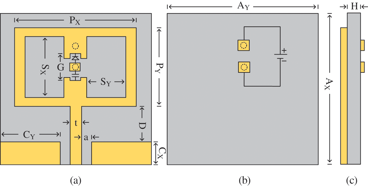
Figure 1: (a) Top, (b) Bottom and (c) Side view of geometrical configuration of the proposed antenna
Fig. 2 illustrates the design steps of the proposed antenna. A rectangular monopole antenna is first designed to operate at 5.5 GHz frequency. This antenna type is chosen for the promising results it provides in terms of bandwidth. This can be explained by analyzing the monopole antenna as being a microstrip antenna whose ground plane is located at infinity [22]. In this case, the layer opposite the radiating element with respect to the substrate is considered as a thick air layer
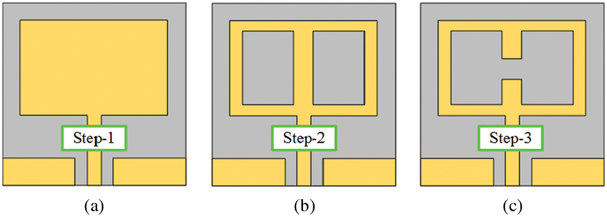
Figure 2: Various design steps generating the proposed antenna
The first step of designing the proposed antenna begins with the design of a rectangular shaped monopole antenna fed by a 50 Ω transmission line.
The length of the basic rectangular radiating element for a given frequency
This expression can be simplified using the formula below [25]:
where c refers to the speed of light in vacuum, which is
where
To calculate the effective dielectric constant
where
The expression for calculating an approximate value of the effective dielectric constant
Fig. 3 illustrates the design steps results of the antenna in terms of return loss. As can be seen, the monopole antenna reported a return loss coefficient of −28 dB at the resonance frequency 5.5 GHz. The bandwidth in this case ranges from 4.8 GHz to 6.5 GHz. i.e., 31% of fractional bandwidth. The second step of antenna design consists of truncating two symmetrical rectangles from the radiating patch as shown in Fig. 2b. The rectangles
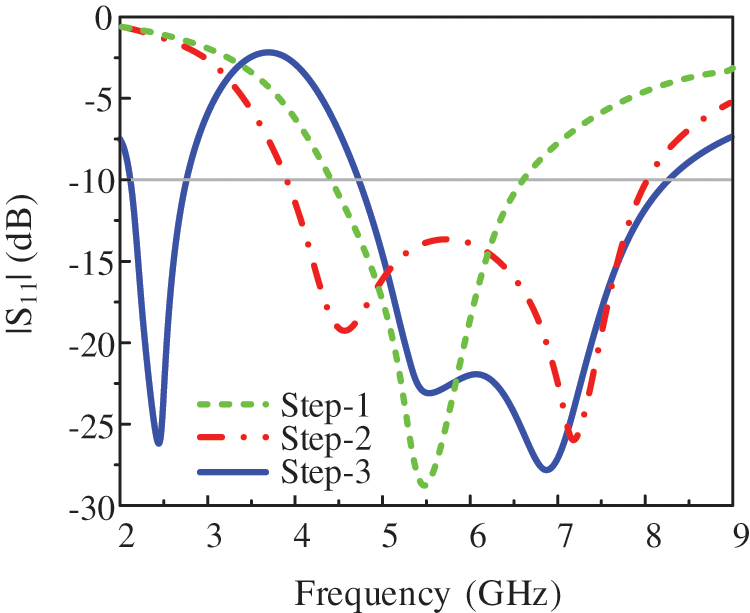
Figure 3: Scattering parameter |S11| (dB) comparison among antenna design steps
The final design step involves introducing a gap in the middle of the metallic strip regarding the Y-axis in order to introduce an RF PIN diode. Theoretically, introducing the gap in the middle of the metallic strip corresponds to the addition of a series capacitor to the total capacitance of the antenna, since the inductance and capacitance are inversely proportional to frequency according to the following formula:
where L and C represent respectively the inductance and capacitance of the antenna.
Therefore, adding a second capacitor in series decreases the capacitance of the resonant circuit, thereby causing the frequency to increase. This can be demonstrated by the return loss results of the third design step illustrated in Fig. 3. The cut off frequencies
PIN diode is used to achieve the reconfigurability feature. In fact, the electrical length of the radiator changes to allow the proper current flow when switching between diode states. Therefore, to design the equivalent model of the PIN diode, lumped Resistance-Inductor-Capacitor (RLC) elements are used. The resistance, capacitance and inductance values of the diode are found in [30]. A thorough parametric study is carried out to determine the optimal PIN diode position to achieve the desired results. In addition, a Direct Current (DC) block 100 pF capacitor is used to uncouple the upper from the lower part of the radiating element shaped as a hollow rectangle. Moreover, to achieve efficient results, via and padding are designed on the back side of the radiating element.
For a better understanding of the different antenna switching states, an equivalent model of the PIN diode (ON and OFF state) as well as a biasing circuit are illustrated in Fig. 4. The forward state of diode is modeled by a resistance of low value (4.7 Ω), in series with an inductance of value 0.15 nH to allow the passage of the current, thus connecting the upper part with the lower part of the radiating element. While the reverse state of the diode is modeled by a resistor of a high value (7 KΩ) connected in parallel with a capacitor (C = 0.017 pF), then connected in series with an inductor having a value of L = 0.15 nH. The high resistance and capacitance values impede the flow of the current in the reverse bias. In addition, the biasing circuit of the diode consists of a DC source (0 V) for OFF state and (3 V) for ON state, mounted in series with 1 KΩ resistor for direct current control, then connected to an inductor (L = 68 nH) to block the alternative currents [31].
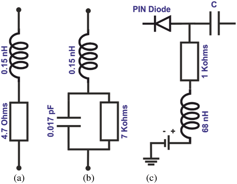
Figure 4: Equivalent model of the diode (a) On state (b) OFF state (c) Biasing circuit of the diode
Fig. 5 depict the return loss results of both ON and OFF states. As we can notice. The antenna operates as a UWB antenna, with two resonance frequencies (4.2 and 7.5 GHz) having respective reflection loss coefficients of −25 and −20 dB. The bandwidth reported in the forward bias case ranges from 3.5 to 8 GHz, which corresponds to a fractional bandwidth of 107% with respect to the first resonance frequency. In another hand, the proposed antenna exhibits multiband behavior in the reverse bias. The disconnection between the upper and lower parts of the radiating elements shifted the operational bandwidth to higher frequencies due to the capacitive nature of the introduced slot. The resonant frequencies in the OFF state shifted from f1 = 4.2 GHz and f2 = 7.5 GHz to f1 = 5.5 GHz and f2 = 6.8 GHz. The respective return loss results are: −23 and −28 dB. Moreover, a new resonant frequency appeared in a lower band at 2.45 GHz characterized by a narrow bandwidth with a respective return loss of −26 dB.
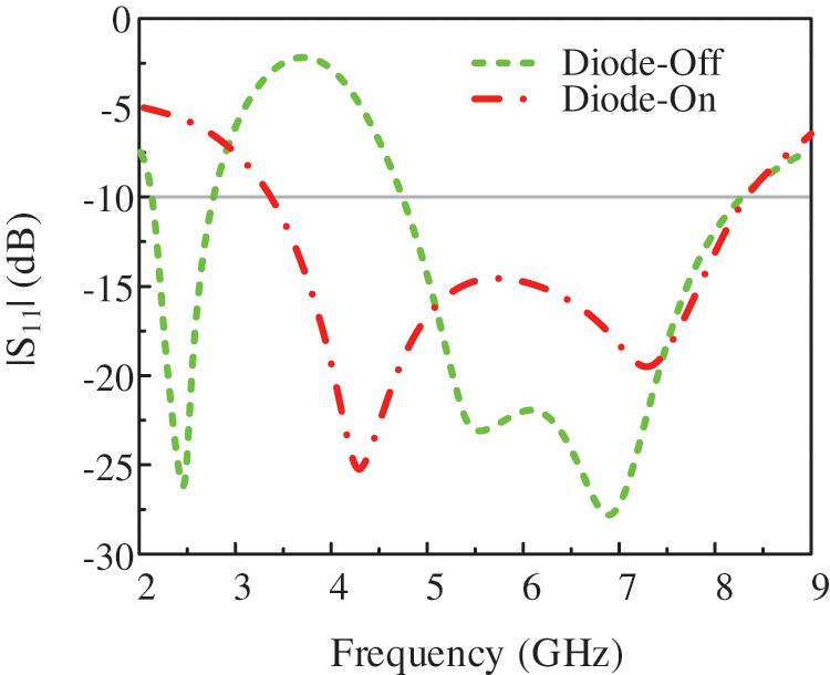
Figure 5: Return loss of the switch diode modes
Providing an equivalent circuit model of an antenna offer useful insight about the performance and design of the antenna, in addition, it enables easy insertion of active elements into the antenna structure. In general, passive antennas are modeled by Foster canonical forms. Magnetic antennas such as loop or quad antennas are modeled by the second canonical foster form, while electric antennas such as dipoles and monopoles are modeled by the first canonical form as shown in Fig. 6 [32]. Monopole antennas are considered passive lossless networks that operate as an open circuit at the DC input signal and are constructed using lumped inductors and capacitors as depicted in Fig. 6a [33].
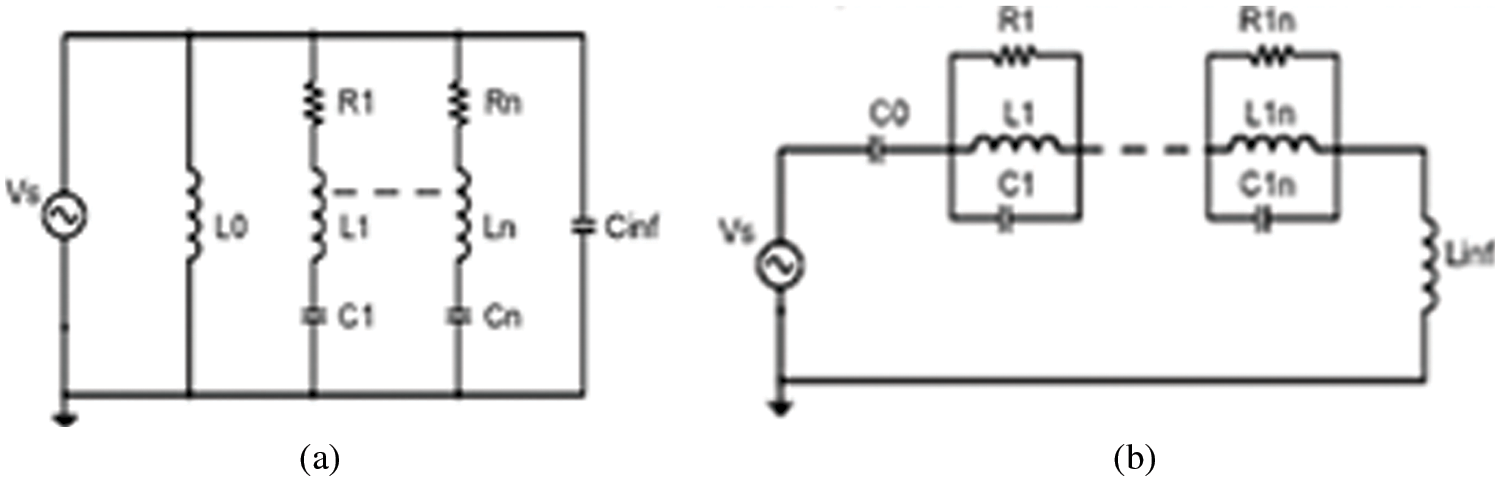
Figure 6: Foster canonical forms (a) Magnetic antennas (b) Electric antennas
Slots introduced into the radiating element perturb the distribution of the current in the antenna; therefore, additional capacitance and inductance are added. Thus, it can be assumed that the slots behave like an Inductor-Capacitor (LC) resonator circuit which is coupled to the antenna. In fact, when an RF signal is transmitted through the introduced slot, a strong coupling arises between the transmission line and the slot around the frequency where the slot resonates. Therefore, to obtain an efficient design for a specific application while considering the unique design variables, an equivalent circuit model is required. In fact, the inductance and capacitance values depend on the size and shape of the slot according to mathematical equations presented in [34]. A general approach is used to represent slots and Defected Ground Structure (DGS) introduced into the antenna. Indeed, it represents larger rectangles by the effective series inductance L, while the narrow slots are represented by a capacitor C in parallel with the inductor L. However, the LC model does not consider neither radiation nor dielectric/conductor losses; therefore, an equivalent loss resistance is added for more accuracy. Thus, the equivalent model of the proposed antenna is illustrated in Fig. 7.
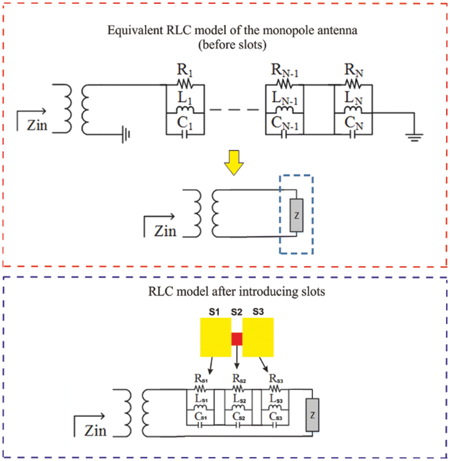
Figure 7: RLC equivalent model of the proposed antenna
3.1 Simulation and Measurement Setup
The proposed antenna is designed and simulated using 3-Dimensional (3D) electromagnetic simulation software HFSS (High Frequency Structure Simulator), used to estimate the electromagnetic behavior of complex designs with indisputable accuracy. This simulator uses the finite element method (FEM) which is adequate for volumetric configurations. In this method, the analyzed structure is fractioned into small units called finite elements depending on the structure to be analyzed. It meshes over the entire volume of solution and resolves the electric field throughout that volume. This method enables the design of complex structures and irregular shapes with a prominent level of accuracy and close agreement with the measured results. To design a high frequency structure “driven” by a source such as monopole antennas, “Driven Modal solution” is used. This solution provide S-matrix results expressed in terms of the incident and reflected powers of waveguide mode. After designing a 3D structure of the proposed antenna, we applied a boundary condition which is a background applied to the region surrounding the geometric model in order to define the behavior of the field across discontinuous boundaries. Afterwards, we designed a SubMiniature version A (SMA) connector to reduce the connector’s impact on antenna performance. To do so, we used wave port excitation which is used for external feedings [35].
Parameter’s optimization is essential to determine the best design variation among a model’s variations. In this design, we used a parametric analysis to perform an automatic optimization of a set of variables instead of a fixed position or size [17]. In order to demonstrate the potential of the proposed antenna, a prototype of the simulated design is fabricated and subjected to experimental measurements. A 50 Ω commercially available SMA connector is used to excite the antenna. For the frequency switching function, we used Skyworks RF PIN diode model SMP-1345 (SC-79). For the PIN-diode biased voltage, we have introduced conducting via on the back of the substrate to connect the diode to the ground. Moreover, a 3 V battery is used in the diode biasing circuit. Fig. 8 shows the prototype of the proposed flexible reconfigurable antenna. For S parameters measurements, a Vector Network Analyzer (VNA) is used. The measurement is carried out by transmitting a signal to the antenna and measuring its response using the VNA. While the far-field measurements were carried out in a shielded RF anechoic chamber. For gain and radiation pattern measurement, we used horn antenna (SGH-Series) as a transmitter, characterized by a typical gain of 24 dBi, in addition, we used gain amplifier to establish an effective transmission of the RF signal, thus, achieving correct results [36].
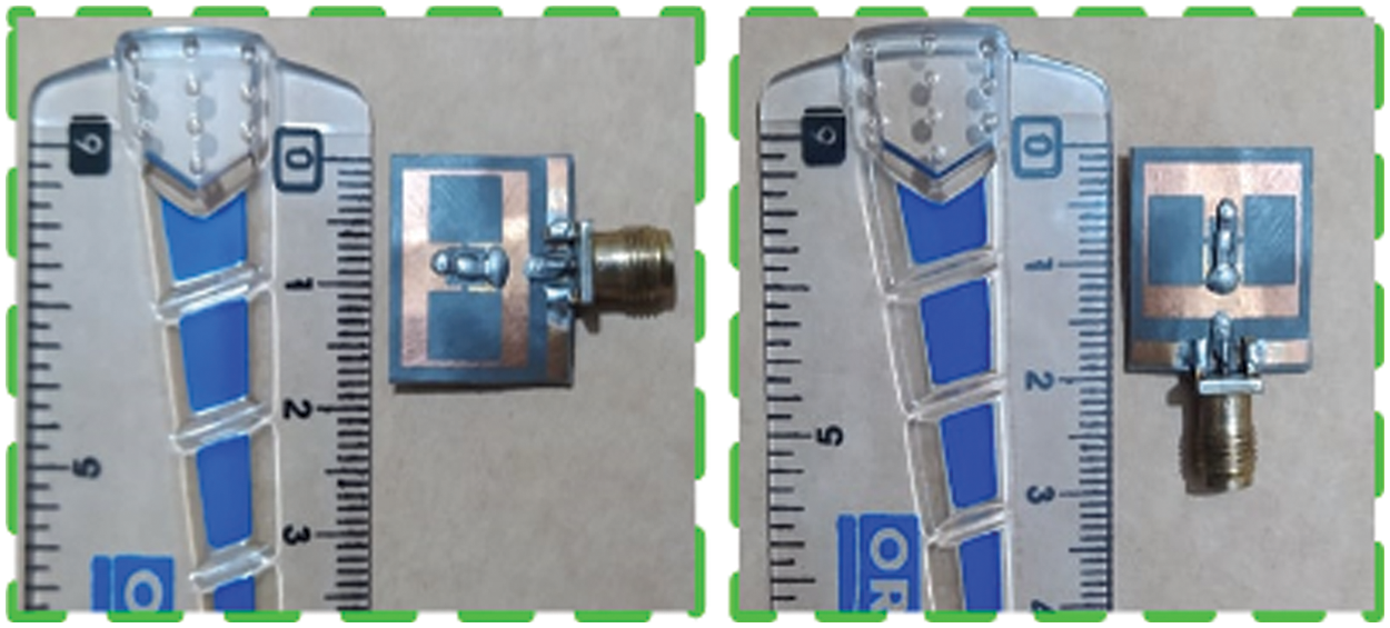
Figure 8: Prototype of the proposed antenna
Fig. 9 illustrates the simulated and measured return loss results of the proposed antenna in forward and reverse bias. As can be noticed, in ON mode, the antenna resonates at two frequencies of 4.2 and 7.2 GHz, with respective return loss coefficients of −26 and −20 dB. The antenna in this case exhibits a UWB behavior with a bandwidth ranging from 3.4 to 8.4 GHz. i.e., 119% of FBW. The measured results show an impedance bandwidth ranging from 3.2 to 8.4 GHz at the same resonant frequencies, with respective S11 values of −27 and −24 dB, which demonstrate the good agreement between simulated and measured results. From the same figure, we can notice that antenna in OFF mode shows a dual band behavior. Indeed, the antenna has a narrow band at lower frequency (2.5 GHz) and a wide band at resonant frequencies (5.5 and 6.8 GHz), with respective values of return loss of −23, −23 and −26 dB. The upper band in this case extends from 4.75 to 8.4 GHz. or 66% of FBW. The same results are reported from the measured plots, showing a small difference in the return loss values, which show the values: −28, −26 and −30 dB, respectively. It is important to note that switching into OFF mode allows the mitigation of the sub-band ranging from 3.2 to 4.75 GHz, which is widely used for many applications and standards, including 5G mid band (3.3–4.2 GHz), Wi-MAX (3.4–3.6 GHz), WLAN IEEE 802.11y-2008 (3.65-3.7 GHz) etc.
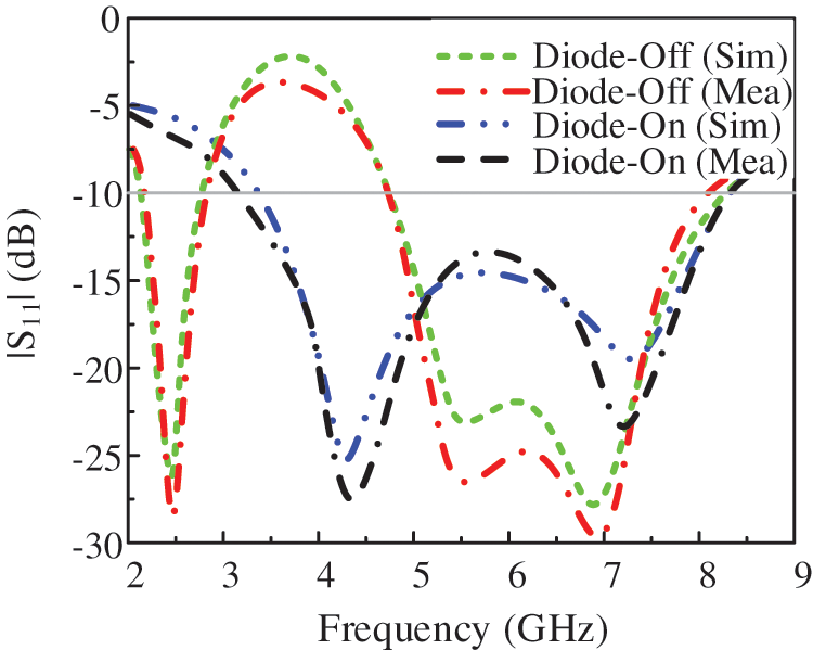
Figure 9: Return loss results of the proposed antenna
In order to validate the potential of a flexible antenna, a conformability test is obviously required. Therefore, we subjected the manufactured prototype to a series of bends along several radii as shown in Fig. 10. To do this, the antenna is wrapped around a cylindrical foam for measurement purposes. Indeed, the radius of the cylinder is chosen, considering that the edges of the antenna must not touch each other. Fig. 11 shows a comparison between the measured results of the conformability test submitted to the antenna. Fig. 11a shows the results of the antenna while the PIN is in the forward bias in both X and Y axes. As can be seen, the antenna exhibits stable bandwidth both under rigid and curved conditions while maintaining adequate return loss results under normal and both curvature conditions (in X-axis and Y-axis). Likewise, it can be deduced from Fig. 11b that the antenna exhibits identical results both under normal and curved conditions when the PIN diode is switched to the OFF state. In fact, the antenna has the same operational bandwidth as well as the same return loss results. However, a negligible yet acceptable variation in the higher resonance frequency is observed. Therefore, the conformability test performed on the proposed antenna demonstrated extraordinarily strong agreement, proving that the antenna is suitable for conformal and non-conformal scenarios.
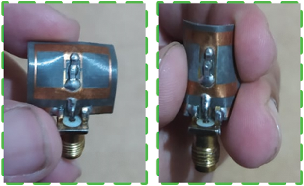
Figure 10: Antenna bending according to X and Y axis
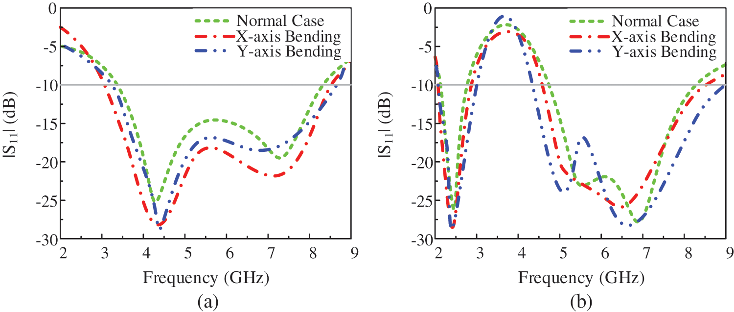
Figure 11: Measured results of conformal antenna (a) ON state (b) OFF state
In order to successfully measure antenna characteristics, near-field measurement is suitable for higher frequencies, while far-field measurement is suitable for low-frequency applications. Thus, in order to validate the potential of the proposed antenna, a study of the radiation pattern of the antenna when the diode is in the OFF state is conducted. Indeed, the performances of the antenna when the antenna exhibits UWB behavior (ON state) do not provide interesting results. Therefore, we will content ourselves with the results of the radiation pattern when the diode is held in the OFF state.
As illustrated in Fig. 12, the antenna exhibits similar behavior in both resonant frequencies (2.45 and 5.8 GHz). In fact, the antenna has an omnidirectional radiation pattern in the H-plan (θ = 90°), while it exhibits a bidirectional pattern in the E-plan (θ = 0°). One can also notice that there is a good agreement between the simulation results and the measurement results since the two curves of the latter coincide perfectly.
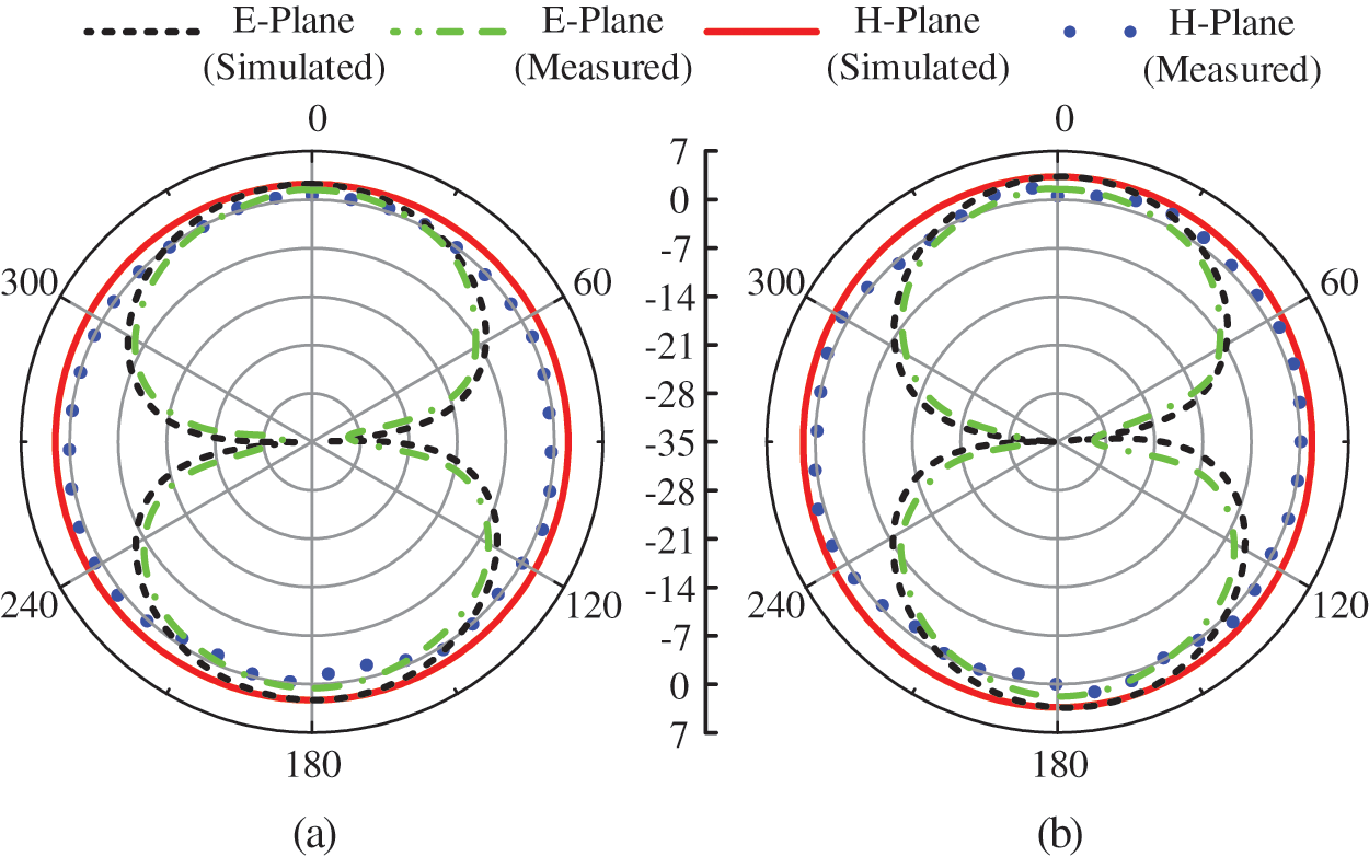
Figure 12: Comparison among simulated and measured radiation efficiency of the antenna (a) 2.45 GHz (b) 5.8 GHz [when diode is in OFF state]
As we mentioned above, the proposed antenna exhibits UWB and dual-band behavior when the PIN diode is in ON and OFF state, respectively. Thus, to analyze the behavior of the antenna in these two modes of operation (ON and OFF), it will be necessary to visualize the gain and the efficiency according to the frequencies. As shown in Fig. 13a, when the diode is kept in the ON state, the antenna exhibits a gain value greater than 3 dB over the entire UWB operating band [3.4–8.4 GHz], peaking at 3.9 at 6 and 7 GHz, then begins to decrease to 3 dB at the upper end of the operating bandwidth. Moreover, we can notice a good agreement between the simulated and measured results, as their curves vary with the same pace over the whole operating band. Regarding the efficiency results, the antenna has a minimum efficiency value at the beginning and end of the operating interval with a minimum value of 90%. Thereafter, the antenna efficiency increases to a maximum value of 94% over a frequency range between 4.8 and 7.5 GHz.
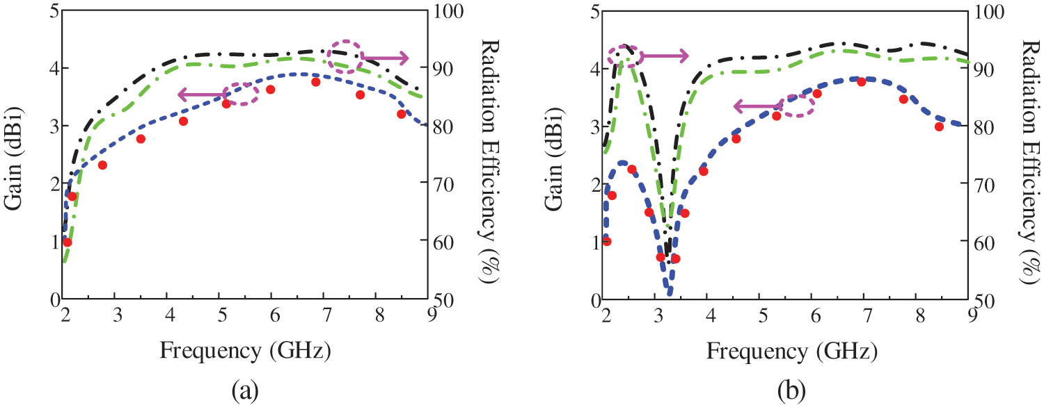
Figure 13: Simulated and measured gain and radiation efficiency of the antenna (a) ON state (b) OFF state
On the other hand, when the diode is switched in the OFF state, it exhibits dual-band behavior. In fact, switching to OFF mode makes it possible to attenuate the sub-band ranging from 3.2 to 4 GHz as illustrated in Fig. 9. Therefore, analyzing the gain results shown in Fig. 13b, we can notice that the antenna exhibits minimum gain on the attenuated frequency band with minimum gain value of 0.2 dB at 3.3 GHz, proving that the antenna successfully attenuates the sub-band [3.2–4 GHz]. Regarding the upper band from 4.75 to 8.4 GHz, the antenna displays a minimum gain value of 3.2 dB in the two extreme frequencies of the passband, then it increases to reach the highest gain value (3.9 dB) over a frequency range of 6.4 to 7.4 GHz. we can also notice that the graphs of simulated and measured results present the same values, proving the validity of the results found.
Finally, the analysis of the plots of the calculated and measured efficiency when the antenna is switched to the OFF state shows that the efficiency of the antenna decreases drastically in the attenuated sub-band. Otherwise, in the other frequencies of the operational band, the antenna has efficiencies of the order of 94%, which proves the potential of the proposed antenna.
3.6 Comparison with Related Work
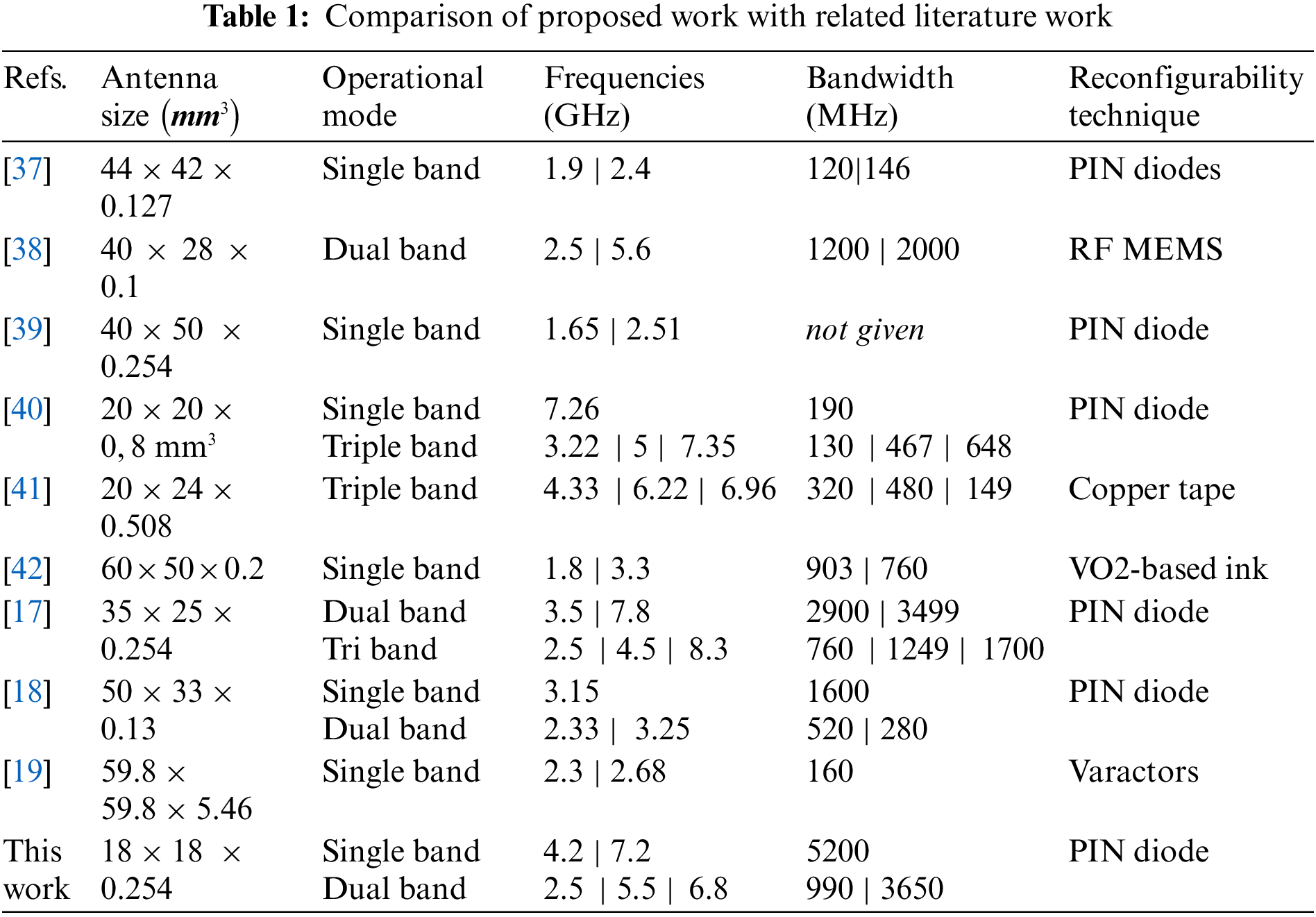
Tab. 1 presents a comparison between the proposed reconfigurable flexible antenna with state-of-the-art antennas, dedicated to the same applications. The presented work overtops the other candidate antennas in terms of size. As can be noticed, our proposed antenna is characterized by an important level of compactness with an overall size of (18 × 18 × 0.254 mm3), which makes it very suitable for miniaturized and flexible devices. Additionally, the antenna is able to switch between UWB and dual-band modes of operation using a single PIN diode, reducing the level of complexity. Moreover, the proposed antenna exhibits the same behavior under both rigid and flexible conditions, making it a potential candidate for modern miniaturized and flexible devices.
A frequency-tunable monopole antenna with a flexibility feature is described in this article. The proposed antenna is characterized by an unusually compact size compared to the wavelength of the antenna. Additionally, the antenna is able to switch between UWB and dual-band behavior using a single PIN diode, which significantly reduces the level of antenna complexity. Indeed, maintaining the PIN diode in the ON state connects the upper part and the lower part of the radiating element by allowing the current to flow, while switching the diode to the OFF state modifies the current distribution, which has the effect of modifying the behavior of the antenna. The introduction of the PIN diode in the radiating element allows switching between several frequencies on demand which are used in the majority of applications and standards, including the 5G mid-band (3.3–4.2 GHz), Wi-MAX (3.4–3.6 GHz), WLAN IEEE 802.11y-2008 (3.65–3.7 GHz) etc. Additionally, the antenna exhibits outstanding intrinsic performance and conformability results, in both simulated and measured results, which demonstrate the antenna’s potential for modern flexible electronic systems
Acknowledgement: The authors would like to acknowledge the financial support received from Taif University Researchers Supporting Project Number TURSP-2020/34, Taif University, Taif, Saudi Arabia, and support from Antenna and Wireless Propagation Group (https://sites.google.com/view/awpgrp).
Funding Statement: This work is supported by Taif University Researchers Supporting Project Number TURSP-2020/34, Taif University, Taif, Saudi Arabia. Also, this work is supported by Antenna and Wireless Propagation Group (https://sites.google.com/view/awpgrp).
Conflicts of Interest: The authors declare that they have no conflicts of interest to report regarding the present study.
1. S. S. Al-Bawri, H. H. Goh, M. S. Islam, H. Y. Wong, M. F. Jamlos et al., “Compact ultra-wideband monopole antenna loaded with metamaterial,” Sensors, vol. 20, no. 3, pp. 796, 2020. [Google Scholar]
2. J. Yeo and J. I. Lee, “Miniaturized wideband loop antenna using a multiple half-circular-ring-based loop structure and horizontal slits for terrestrial DTV and UHD TV applications,” Sensors, vol. 21, no. 9, pp. 2916, 2021. [Google Scholar]
3. K. S. Kim, I. J. Hwang, B. K. Ahn, H. Y. Cho and J. W. Yu, “Gain-enhanced cavity-backed cross slot antenna with truncated ground walls,” IEEE Transactions on Antennas and Propagation, vol. 68, no. 6, pp. 4293–4301, 2020. [Google Scholar]
4. Y. Q. Guo, Y. M. Pan, S. Y. Zheng and K. Lu, “A singly-fed dual-band microstrip antenna for microwave and millimeter-wave applications in 5G wireless communication,” IEEE Transactions on Vehicular Technology, vol. 70, no. 6, pp. 5419–5430, 2021. [Google Scholar]
5. R. L. Haupt and M. Lanagan, “Reconfigurable antennas,” IEEE Antennas and Propagation Magazine, vol. 55, no. 1, pp. 49–61, 2013. [Google Scholar]
6. E. Motovilova and S. Y. Huang, “A review on reconfigurable liquid dielectric antennas,” Materials, vol. 13, no. 8, pp. 1863, 2020. [Google Scholar]
7. A. Zaidi, W. A. Awan, N. Hussain and A. Baghdad, “A wide and tri-band flexible antennas with independently controllable notch bands for sub-6-GHz communication system,” Radioengineering, vol. 29, no. 1, pp. 44–51, 2020. [Google Scholar]
8. A. Ghaffar, W. A. Awan, N. Hussain and X. J. Li, “A compact octa-band frequency reconfigurable antenna for wireless applications,” Mathematics, vol. 9, no. 13, pp. 1557, 2021. [Google Scholar]
9. W. A. Awan, S. I. Naqvi, W. A. E. Ali, N. Hussain, A. Iqbal et al., “Design and realization of a frequency reconfigurable antenna with wide, dual, and single-band operations for compact sized wireless applications,” Electronics, vol. 10, no. 11, pp. 1321, 2021. [Google Scholar]
10. M. Alharbi, M. A. Alyahya, S. Ramalingam, A. Y. Modi, C. A. Balanis et al., “Metasurfaces for reconfiguration of multi-polarization antennas and van atta reflector arrays,” Electronics, vol. 9, no. 8, pp. 1262, 2020. [Google Scholar]
11. T. Prakash, R. K. Chaudhary and R. K. Gangwar, “Pattern-reconfigurable antenna in azimuth plane using SP3T reconfigurable switching network,” IET Microwaves, Antennas & Propagation, vol. 15, no. 1, pp. 62–68, 2021. [Google Scholar]
12. M. K. Shereen and M. I. Khattak, “A hybrid reconfigurability structure for a novel 5G monopole antenna for future mobile communication,” Frequenz, vol. 75, no. 3, pp. 71–82, 2021. [Google Scholar]
13. M. K. Shereen, M. I. Khattak and M. Al-Hasan, “A frequency and radiation pattern combo-reconfigurable novel antenna for 5G applications and beyond,” Electronics, vol. 9, no. 9, pp. 1372, 2020. [Google Scholar]
14. S. G. Kirtania, A. W. Elger, M. Hasan, A. Wisniewska, K. Sekhar et al., “Flexible antennas: A review,” Micromachines, vol. 11, no. 9, pp. 847, 2020. [Google Scholar]
15. S. G. Kirtania, B. A. Younes, A. R. Hossain, T. Karacolak and P. K. Sekhar, “CPW-fed flexible ultra-wideband antenna for IoT applications,” Micromachines, vol. 12, no. 4, pp. 453, 2021. [Google Scholar]
16. A. Hassan, S. Ali, G. Hassan, J. Bae and C. H. Lee, “Inkjet-printed antenna on thin PET substrate for dual band Wi-fi communications,” Microsystem Technologies, vol. 23, no. 8, pp. 3701–3709, 2017. [Google Scholar]
17. N. Hussain, W. A. Awan, S. I. Naqvi, A. Ghaffar, A. Zaidi et al., “A compact flexible frequency reconfigurable antenna for heterogeneous applications,” IEEE Access, vol. 8, pp. 173298–173307, 2020. [Google Scholar]
18. K. Saraswat and A. R. Harish, “Flexible dual-band dual-polarised CPW-fed monopole antenna with discrete-frequency reconfigurability.” IET Microwaves, Antennas & Propagation, vol. 13, no. 12, pp. 2053–2060, 2019. [Google Scholar]
19. R. B. V. B. Simorangkir, Y. Yang, K. P. Esselle and B. A. Zeb, “A method to realize robust flexible electronically tunable antennas using polymer-embedded conductive fabric,” IEEE Transactions on Antennas and Propagation, vol. 66, no. 1, pp. 50–58, 2017. [Google Scholar]
20. H. F. Abutarboush and A. Shamim, “A reconfigurable inkjet-printed antenna on paper substrate for wireless applications,” IEEE Antennas and Wireless Propagation Letters, vol. 17, no. 9, pp. 1648–1651, 2018. [Google Scholar]
21. L. Aguni, A. E. Yassini, S. Chabaa, S. Ibnyaich and A. Zeroual, “Design of a symmetric CPW-fed patch antenna for WLAN/WIMAX applications using ANN,” Wireless Personal Communications, vol. 115, no. 1, pp. 439–456, 2020. [Google Scholar]
22. K. P. Ray, “Design aspects of printed monopole antennas for ultra-wide band applications,” International Journal of Antennas and Propagation, vol. 2008, Article ID 713858, 2008. [Google Scholar]
23. H. M. Lee and W. S. Choi, “Effect of partial ground plane removal on the radiation characteristics of a microstrip antenna,” Wireless Engineering Technology, vol. 4, no. 1, 2013. [Google Scholar]
24. C. A. Balanis, Antenna Theory: Analysis and Design, United State of America, John Wiley & Sons, 2015. [Google Scholar]
25. A. Hassanien, W. Swelam and M. H. A. E. Azeem, “16 × 8 wideband microstrip planar array antenna for E-band millimeter-wave 5G high speed WLAN and broadband internet applications,” in IEEE Int. Symp. on Antennas and Propagation & USNC/URSI National Radio Science Meeting, Spokane, Washington, United States, pp. 2613–2614, 2017. [Google Scholar]
26. A. M. Lozano, C. B. Angulo, H. G. Martínez, R. G. Mazón, G. T. Penalva et al., “Uwb-printed rectangular-based monopole antenna for biological tissue analysis,” Electronics, vol. 10, no. 3, pp. 304, 2021. [Google Scholar]
27. V. V. Thakare and P. K. Singhal, “Bandwidth analysis by introducing slots in microstrip antenna design using ANN,” Progress in Electromagnetics Research M, vol. 9, pp. 107–122, 2009. [Google Scholar]
28. S. Rekha and M. Nesasudha, “Bandwidth improvement of a rear end slot antenna on a substrate integrated waveguide cavity,” IOP Conference Series: Materials Science and Engineering, vol. 247, no. 1, pp. 12003, 2017. [Google Scholar]
29. S. I. H. Shah, S. Bashir, A. Altaf and S. D. H. Shah, “Compact multiband microstrip patch antenna using defected ground structure (DGS),” in XIXth Int. Seminar/Workshop on Direct and Inverse Problems of Electromagnetic and Acoustic Wave Theory (DIPED), Tbilisi, Georgia, Azerbaijan, pp. 96–99, 2014. [Google Scholar]
30. Skyworks|Home. [Online]. Available: https://www.skyworksinc.com/ (accessed on 29 September 2021). 2021. [Google Scholar]
31. A. Iqbal, A. Smida, N. K. Mallat, R. Ghayoula, I. Elfergani et al., “Frequency and pattern reconfigurable antenna for emerging wireless communication systems,” Electronics, vol. 8, no. 4, pp. 407, 2019. [Google Scholar]
32. S. Palud, F. Colombel, M. Himdi and C. L. Meins, “Circuit modeling of a small broadband conical antenna,” IEEE Antennas and Wireless Propagation Letters, vol. 8, pp. 96–99, 2009. [Google Scholar]
33. A. Pandey, Practical Microstrip and Printed Antenna Design, United State of America, Artech House, 2019. [Google Scholar]
34. D. Guha and Y. M. M. Antar, in Microstrip and Printed Antennas: New Trends, Techniques and Applications, United State of America, John Wiley & Sons, 2011. [Google Scholar]
35. Ansys|Engineering Simulation Software. [Online]. Available: https://www.ansys.com/ (last assessed on 1 March 2021). 2021. [Google Scholar]
36. W. A. Awan, A. Zaidi, M. Hussain, N. Hussain and I. Syed, “The design of a wideband antenna with notching characteristics for small devices using a genetic algorithm,” Mathematics, vol. 9, no. 17, pp. 2113, 2021. [Google Scholar]
37. Z. Zhu, P. Wang, S. You and P. Gao, “A flexible frequency and pattern reconfigurable antenna for wireless systems,” Progress in Electromagnetics Research Letters, vol. 76, pp. 63–70, 2018. [Google Scholar]
38. B. P. Nadh, B. T. P. Madhav, M. S. Kumar, T. A. Kumar, M. V. Rao et al., “MEMS-Based reconfigurable and flexible antenna for body-centric wearable applications,” Journal of Electromagnetic Waves and Applications, vol. 36, pp. 1–15, 2022. [Google Scholar]
39. A. Ghaffar, X. J. Li, W. A. Awan, A. H. Naqvi, N. Hussain et al., “A flexible and pattern reconfigurable antenna with small dimensions and simple layout for wireless communication systems operating over 1.65–2.51 GHz,” Electronics, vol. 10, no. 5, pp. 601, 2021. [Google Scholar]
40. B. R. S. Reddy, N. K. Darimireddy, C. W. Park and A. Chehri, “Performance of reconfigurable antenna fabricated on flexible and nonflexible materials for band switching applications,” Energies, vol. 14, no. 9, pp. 2553, 2021. [Google Scholar]
41. A. Ahmad, F. Arshad, S. I. Naqvi, Y. Amin, H. Tenhunen et al., “Flexible and compact spiral-shaped frequency reconfigurable antenna for wireless applications,” IETE Journal of Research, vol. 66, no. 1, pp. 22–29, 2020. [Google Scholar]
42. S. Yang, M. Vaseem and A. Shamim, “Fully inkjet-printed VO2-based radio-frequency switches for flexible reconfigurable components,” Advanced Materials Technologies, vol. 4, no. 1, pp. 1800276, 2019. [Google Scholar]
 | This work is licensed under a Creative Commons Attribution 4.0 International License, which permits unrestricted use, distribution, and reproduction in any medium, provided the original work is properly cited. |