| Computers, Materials & Continua DOI:10.32604/cmc.2022.027975 | |
| Article |
Design of Multi-Valued Logic Circuit Using Carbon Nano Tube Field Transistors
1Department of Electronics and Communication Engineering, Koneru Lakshmaiah Education Foundation, Aziz Nagar, Hyderabad, 500075, Telangana, India
2Department of Electronics and Communication Engineering, RGM College of Engineering and Technology, Nandyal, 518501, Andhra Pradesh, India
3Department of Electrical and Electronics Engineering, Koneru Lakshmaiah Education Foundation, Vaddeswaram, Guntur, 522502, Andhra Pradesh, India
*Corresponding Author: L. Koteswara Rao. Email: lkraoklh@gmail.com
Received: 30 January 2022; Accepted: 05 May 2022
Abstract: The design of a three-input logic circuit using carbon nanotube field effect transistors (CNTFETs) is presented. Ternary logic must be an exact replacement for dual logic since it performs straightforwardly in digital devices, which is why this design is so popular, and it also reduces chip area, both of which are examples of circuit overheads. The proposed module we have investigated is a triple-logic-based one, based on advanced technology CNTFETs and an emphasis on minimizing delay times at various values, as well as comparisons of the design working with various load capacitances. Comparing the proposed design with the existing design, the delay times was reduced from 66.32 to 16.41 ps, i.e., a 75.26% reduction. However, the power dissipation was not optimized, and increased by 1.44% compared to the existing adder. The number of transistors was also reduced, and the product of power and delay (P*D) achieved a value of 0.0498053 fJ. An improvement at 1 V was also achieved. A load capacitance (fF) was measured at different values, and the average delay measured for different values of capacitance had a maximum of 83.60 ps and a minimum of 22.54 ps, with a range of 61.06 ps. The power dissipations ranged from a minimum of 3.38 µW to a maximum of 6.49 µW. Based on these results, the use of this CNTFET half-adder design in multiple Boolean circuits will be a useful addition to circuit design.
Keywords: Carbon nanotube field effect transistor (CNTFET); multivalued logic (MVL); ternary adder; Hewlett simulation program with integrated circuit emphasis (HSPICE); chirality (nm); adder
The analysis of digital circuits is accomplished using dual-valued logic, i.e., 0 and 1, T and F in Boolean arithmetic. Multivalued logic (MVL) can be matched with the classical arithmetical modification of finite variables [1]. In the general development of new binary circuit chips, 70% of the area is devoted to interconnections, 20% to insulation, and only 10% to transistors. With these considerations in mind, we have devised a new approach to reducing power dissipation and interface complexity, i.e., ternary (multivalued) or three-input logic, which has different possible future uses compared to dual logic for implementing digital systems, and it can also be a solution for reducing power dissipation [2,3]. For example, by adopting three-input logic, this arrangement provides flexibility and simplicity in the digital mode of operation and reduces the various problems associated with circuit connections and the area of the chip itself [4]. Extensive research into the implementation of three-input logic circuits has been conducted [5–7]. By using an efficient MVL implementation, the area of the chip and power dissipation can be reduced by 50% or more, and also in MVL circuits, as each wire can transmit more information than when using binary logic, the number of interconnections required to implement logical functions is reduced, and, hence, the complexity of the chip is reduced [8]. There are two different variants of MVL circuits in existence that use metal oxide semiconductor (MOS) technology and current-and voltage-mode type circuits [9]. In multi-threshold complementary metal oxide semiconductor (CMOS) circuits, voltage-mode MVL circuits play a more important role [10,11].
Carbon nanotubes (CNTs) are huge cylindrical molecules made up of a hexagonal arrangement of hybridized carbon atoms that can be made by rolling up a single sheet of graphene single-walled carbon nanotubes (SWCNTs).
CNTs have received more specific attention in the field of electronics because of their structure and excellent physical properties [12–14]. Numerous recent studies have explored carbon nanotube field effect transistors (CNTFETs) in basic gate arrangements, giving importance to their working and performance compared with MOS technology [15–17]. The CNTFET circuit implementation also includes dual-logic gates [18], three-input logic gates, MVL [19], and binary memory cells [20]. The use of carbon nanotubes for MVL has received much attention since the threshold voltage of CNTFETs may be maintained with selected CNTFET chiral vectors [21–23]. In MVL, we have three different stages in which more specific parameters of a circuit can be specified [24]. Different adders, multipliers, and memory circuits, as well as logic circuits, are developed in order to achieve less delay and reduced power consumption. By controlling the diameter of the CNT, the electronic switch threshold voltage of CNTs can be solved. Therefore, a multi-threshold design is used in the process, in combination with CNTs of various diameters (and, therefore, “chirality”) in the CNTFETs [25–27]. As our design employs three-valued logic exactly similarly to this, we have another type of approach: in the digital world, there are digital photographs and movies, and illegal users can readily modify, reproduce, and share 3-D meshes [28]. One concept uses three-input logic to a binary decoder, which minimizes the amount of computing power needed to create a three-input logic adder. This adder circuit provides different parameters, such as delay, power, the product of power delay, and also, we can see the minimum transistor count used compared to a recent reported study [29]. A modified three-input logic design approach is proposed in this paper, and a large quantity of simulation data are presented. Using arithmetic circuit designs developed by the new CNTFET-based gates, the Hewlett simulation program with integrated circuit emphasis (HSPICE) results reveal desirable improvements in various aspects, such as speed and power consumption [30,31].
The paper is arranged as follows: Section 2 discusses carbon-based nano-type field effect transistors (FETs) and their suitability for three-input logic; Section 3 describes three-input logic itself; Section 4 describes the proposed three-input logic half adder; and, finally, Section 5 discusses the conclusions drawn from the results of our study.
2 Carbon-based Nano-type FET and Its Suitability for Three-input Logic
“Simple and efficient design, reduced memory and inner connectivity, reduced on-chip area, serial and parallel transfer of data, increased potential for maximizing speed, decreased activity of switching, and applications of types of mathematical and Boolean functions on a single chip are all general uses of MVL” [32]. Our study focused on ternary logic, that is, an MVL with three states: zero (0), one (1), and two (2), which represent low, medium, and high ternary values, respectively. CNTFETs use semiconducting single-walled CNTs in particular in the manufacture of electronic devices. A CNT consists of one cylinder and is called a single-walled CNT, a design that is a preferred alternative used in the manufacture of current metal oxide semiconductor field effect transistors (MOSFETs). The arrangement of atom angles along the tube identifies an SWCNT as either a conductor or a semiconductor. This is preferred as the chirality vector, which represents a pair (n, m). According to a popular theory, the indexes indicate whether a CNT is a semiconducting material or metallic (n, m). The nanotube is metallic if n = m or n − m = 3i, where i is an integer; the tube is semiconducting otherwise. The diameter of a CNT is expressed by Eq. (1) [33]:
The carbon atom distance of each and every nearby atom is given as a0 = 0.142 nm. A schematic diagram of a CNTFET is shown in Fig. 1. The CNTFET has four connection options, just like a regular silicon device. The channel area is given as undoped semiconducting nanotubes under the gate, and connecting to the “heavily impure” CNT segments between the gate area and the drain/source allows for a low series resistance when it is in the ON state. The transistor is electrostatically turned “on” or “off” as the potential of the gate increases. The CNTFET’s I–V characteristics are the same as those of the MOSFET. To switch a transistor ON, the voltage required is called the threshold voltage. The intrinsic threshold voltage of the CNT channel is averaged to the first order, and the function for its diameter is given by Eq. (2):
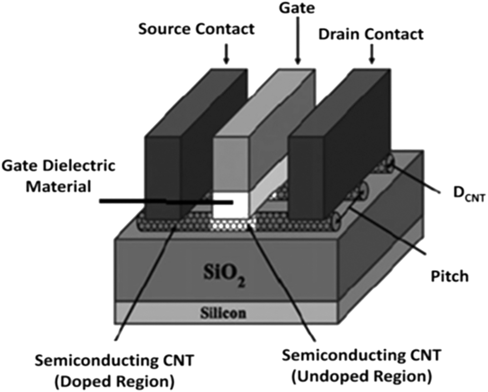
Figure 1: Schematic representation of a CNTFET using multiple carbon-type nanotubes in the channel [6]
We have a0 = 2.49 Å for the carbon-to-carbon distance and V = 3.033 eV for the carbon bond energy, where D is the diameter of the CNT and e is the unit electron charge in tight bonding.
Three input logic CNTFETs were employed in this application. Fig. 2 gives the I–V graph of a CNTFET with various chiral vectors. As a result, the characteristics of a CNTFET are similar to those of MOSFET. The graph shows the I–V characteristics for different values of chiral vectors, such as (19,0), (15,0), (13,0), and (10,0).
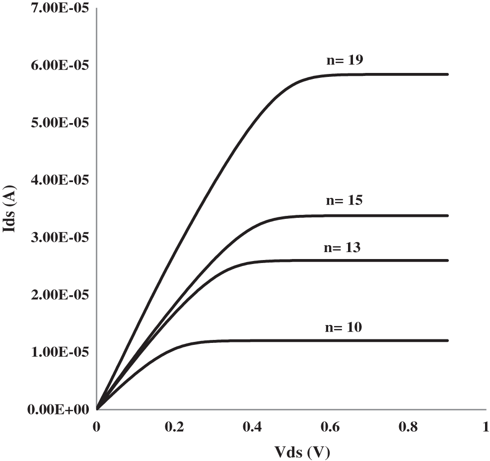
Figure 2: HSPICE simulation of Stanford’s small model generated CNT characteristics [33]
3 Review of Three-input Logic Adder
The fundamentals of ternary logic and how it is represented in terms of voltage levels may be represented by a few input logic gates that can be used to create adder circuits. The various ternary half-adder (THA) design implementations are evaluated and discussed below. Some design options use ternary logic gates (decoder-encoder), a combination of ternary and binary logic, multiplexers, transmission gates, and other techniques [34]. The most recent initiative represents an adder circuit with voltage levels 0, VDD/2, and VDD, used to represent the logic states zero (0), one (1), and two (2), respectively. A three-input logic adder based on Lin et al. [35] was constructed and is described as a simulated adder module. In their design, they replaced part of a three-input logic family with a dual-logic family, as shown in Fig. 3. This replacement reduced the switch (transistors) count and hence gave improved results.
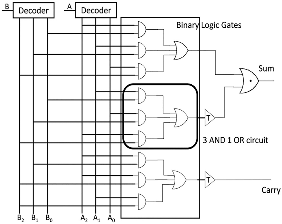
Figure 3: Dual-logic gates replace a part of the three-input logic in a three-input half adder [35]
4 Proposed Three-input Logic Half Adder
In the proposed design, a simple approach is considered for designing an efficient adder, and this approach is based on two-output/three-input logic to a binary decoder circuit. In an adder, the generation of sum and carry reduces the circuit’s complexity.
In the proposed design, A and B are the decoders, and if we allow a single input to a decoder, it will have multiple outputs. In that respect, A and B, which are inputs for the decoder, and the sum and carry circuits, are the operational circuits through which the sum and carry outputs are received. The proposed design for the decoder is rearranged by connecting 1-input and 2-output three-input logic to the dual-input logic decoder. These binary-decoded outputs are used for calculating the values (Sum1, Sum2) and the middle (Cm) in the dual-logic circuit. Lastly, using the selected encoder circuits, the dual-logic intermediate sums and carry are modulated back to the three-input logic. The circuitry of the proposed module is shown in Fig. 4.
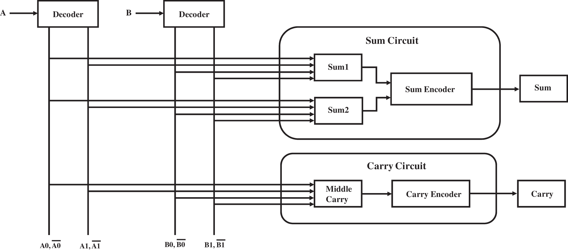
Figure 4: Schematic model of the proposed half adder
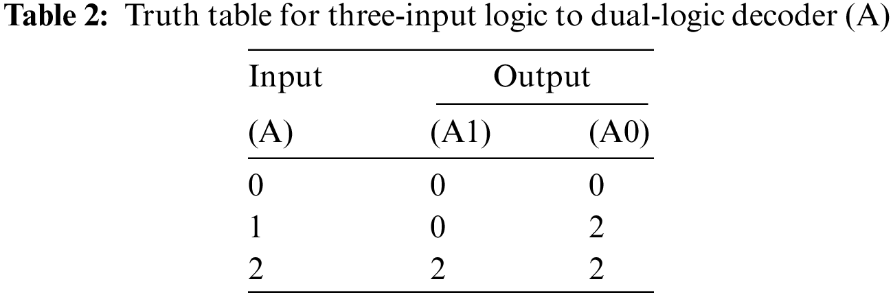
From Tab. 2 above, for a single input, we can see dual outputs; there are inputs such as A(0,1,2), and from this, outputs such as A1(0,0,2) and A0(0,2,2).
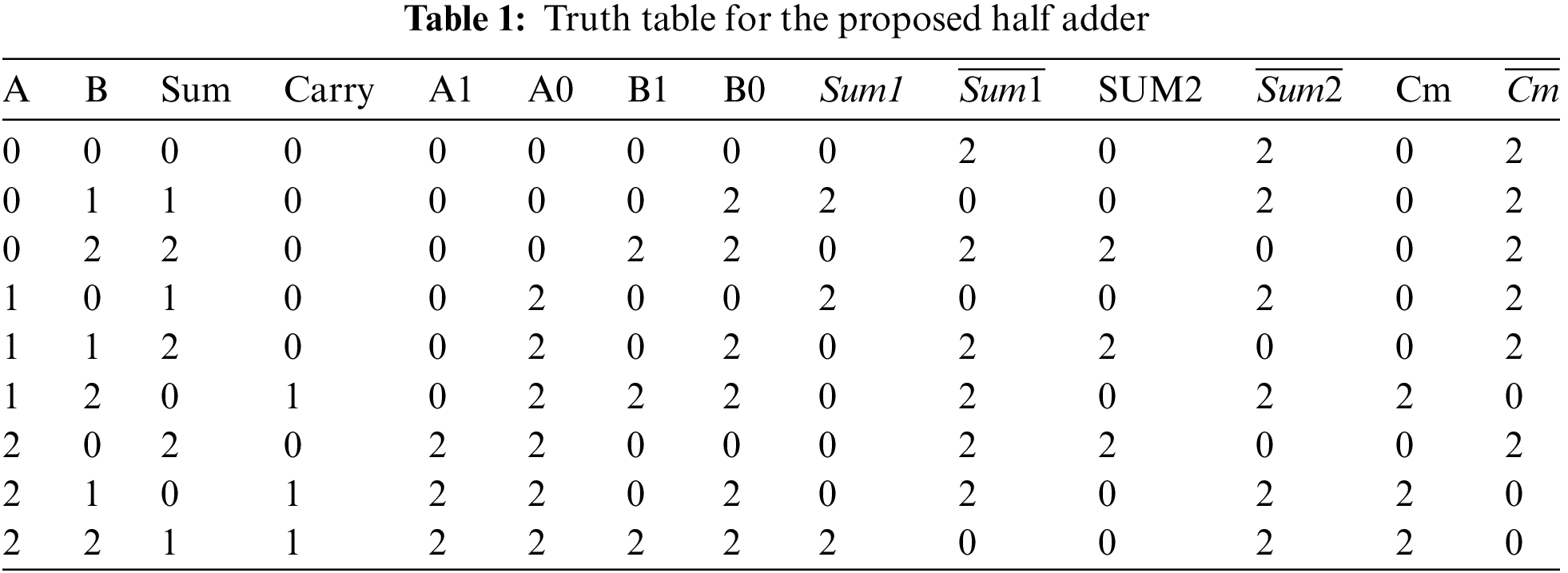
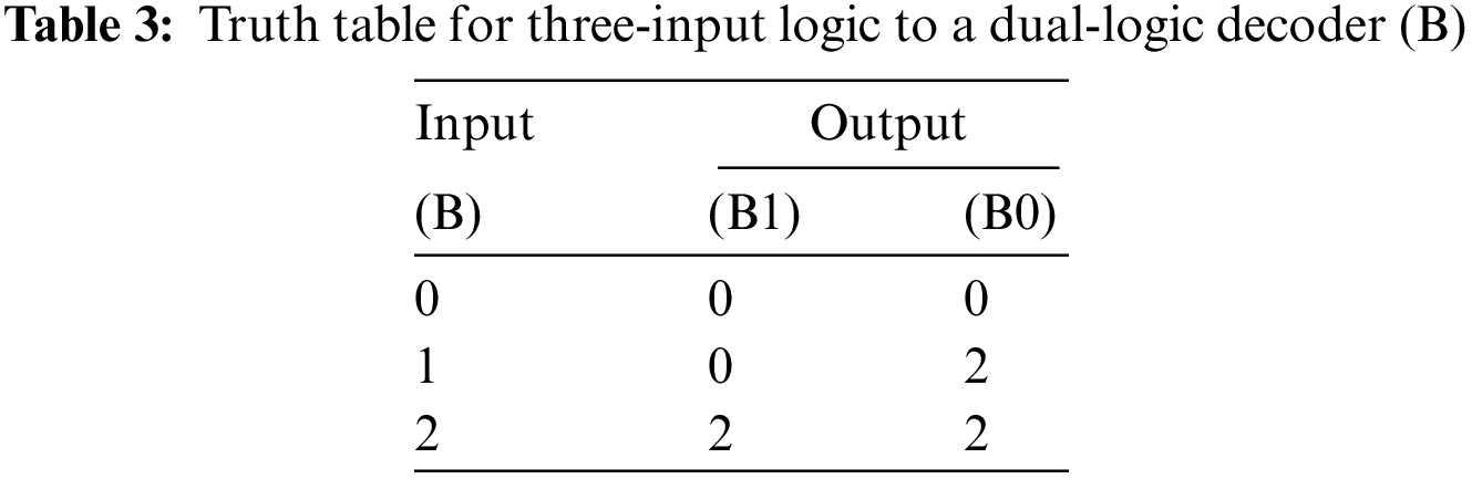
For single inputs, dual outputs can be seen in Tab. 3; there are inputs such as B(0,1,2) and outputs such as B1(0,0,2) and B0(0,2,2).
4.2 Three-Input Logic to Dual-input Decoder
If we go with a three-input logic circuit, the signals analyzed under the three modes, low, medium, and high, can be taken as 0, 1, and 2, respectively. A0 and A1 are the decoder circuit outputs for the three-input signal A (Tab. 2). Fig. 5a gives A0 and A1, and their bars are produced by switch-level decoder circuits. For the design of CNTFETs, we took into account the CNTs of three chiral vector variants: (19, 0), (13, 0), and (10, 0). The diameters of the three CNTs were obtained from Eq. (1) as 1.487, 1.018, and 0.783 nm, respectively. Next, using Eq. (2), the CNTFET threshold voltages were found to be 0.293, 0.428, and 0.557 V, respectively. Approximate switching of transistors can be seen, and the remaining outputs were obtained by different types of CNTs. T′2 and T′5 are TRUE for a complex input value of A of 1 (0.5 V), whereas T′1 and T′6 are FALSE. As a result, the values for A0′ are FALSE (0 V) and for A1′ are TRUE (1 V). It can be seen that transistors T3, T8, and T4, T7 are TRUE and FALSE, respectively, and that the values for A0 are high (1 V) and for A1 are low (0 V). The outputs were obtained for input values of 0 and 2. The same operation is applicable to the input block three-input logic circuit to the binary decoder circuit in Fig. 5b.
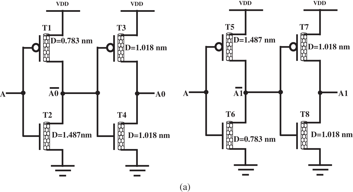
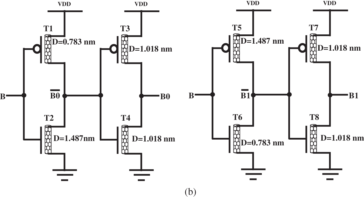
Figure 5: (a) A-input block three-input logic to binary decoder circuit; (b) B-input block three-input logic to binary decoder circuit
Tab. 1 lists the truth table for a previously studied adder, as well as dual-decoded signals A1, A0 and B1, B0, sums (Sum1, Sum2), and a carry signal (Cm) in between. It can be seen from the simulation mode and the results that Sum is 1 only for the three inputs A1, A0, B1 and B0, namely, (2, 2, 2, 2), (0, 2, 0, 0), and (0, 0, 0, 2). Similarly, for those exact input/output combinations, the Sum1 column in Tab. 1 has the result 2.
The sum is just 2 for the combinations A1, A0 and B1, B0, namely, (0, 0, 2, 2), (0, 2, 0, 2), and (2, 2, 0, 0). The same is underlined in Tab. 1’s Sum2 column, which has an output value of 2 for those particular input combinations. Sum1 and Sum2 have the following Boolean expressions:
By using Sum1 and Sum2, we have two circuit possibilities, which are given in Figs. 6a and 6b, respectively.
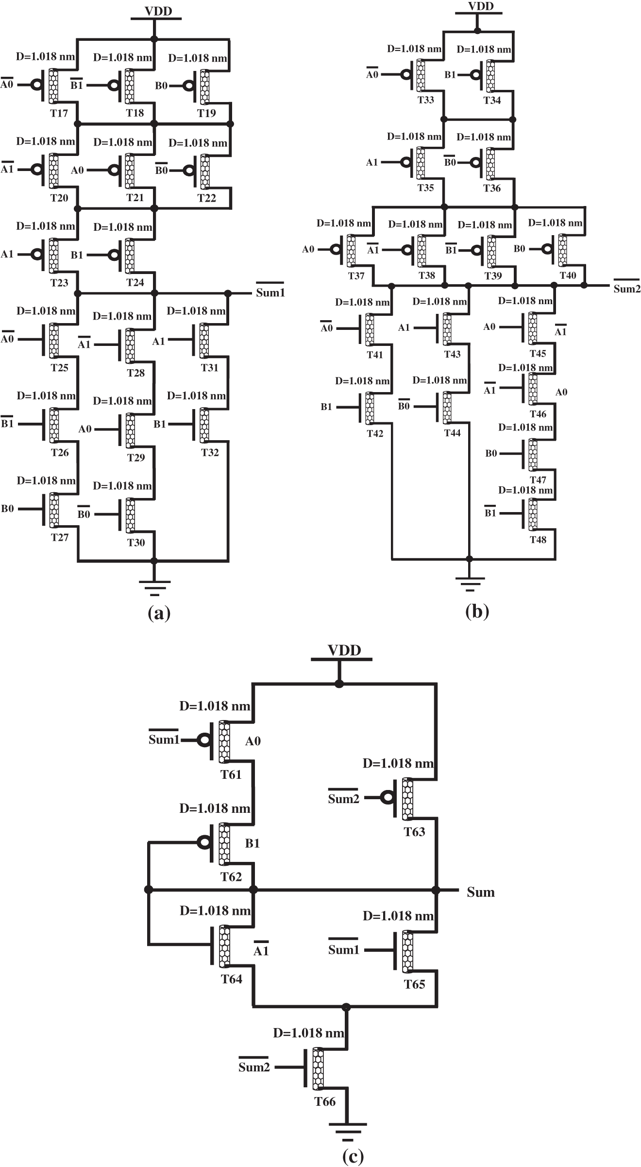
Figure 6: (a) Sum circuit Sum1; (b) sum circuit Sum2; (c) encoder
The results obtained from these dual circuits form a dual input to the three-input encoders, through which the three-input logic output can be observed. The circuit for the encoder in shown in Fig. 6c, and the types of transistor operations are determined by the values of
As listed in Tab. 1, carry is 1 for three of B1, B0 A1, A0, i.e., (2, 2, 0, 2), (0, 2, 2, 2), and (2, 2, 2, 2), respectively. The Cm middle carry can be found from Tab. 1, 13th column. Fig. 7 shows the circuit of carry generator unit. The logical expression for the
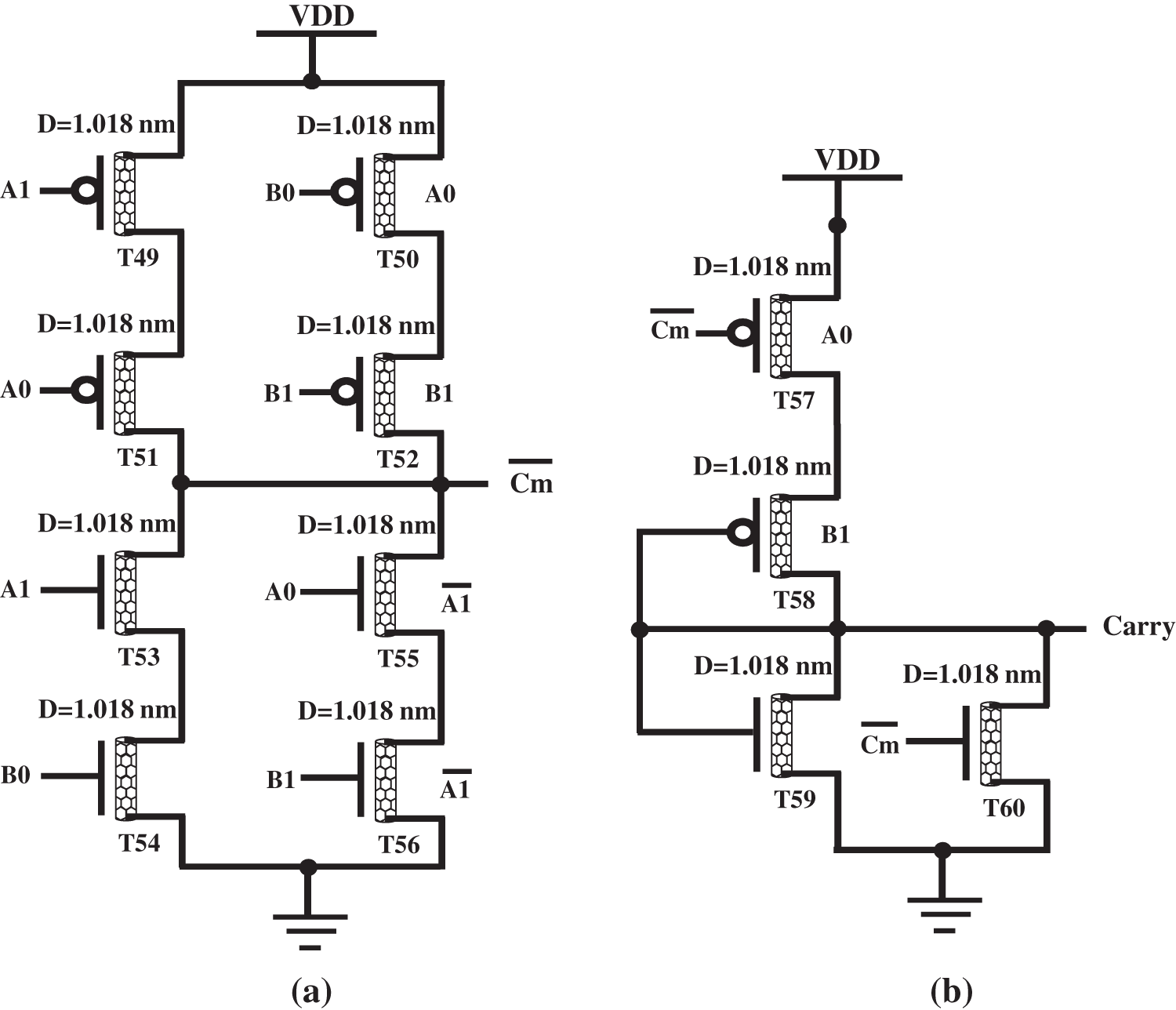
Figure 7: Carry generator circuit: (a)
From the waveform, it can clearly be seen that, for inputs (AB) = (00), Sum and Carry are (00), and for input A(0.5) and input B(0.5), Sum is 2 and Carry is 0, and the process follows for the different combinations of the waveform. According to Tab. 1, the above waveform is generated for ternary logic values such as (0,0.5,1), and the simulations were carried out using the HSPICE tool. The waveform of new decoder-based half-adder circuit is shown in Fig. 8.
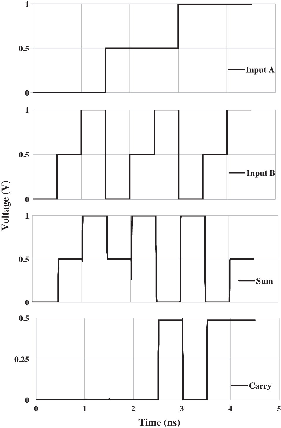
Figure 8: Waveform of the new decoder-based half-adder circuit
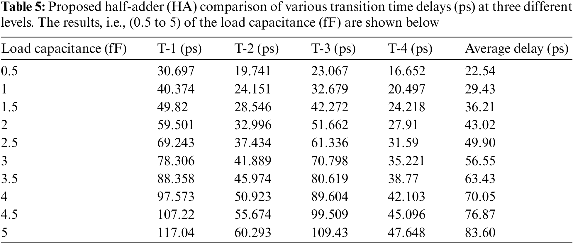
Fig. 9 shows the variation of average delay, measured in picoseconds (ps), with load capacitance, measured in femtofarads (fF). From Fig. 9, it can easily be seen that if the load capacitance is maximized, the average delay is also maximized.
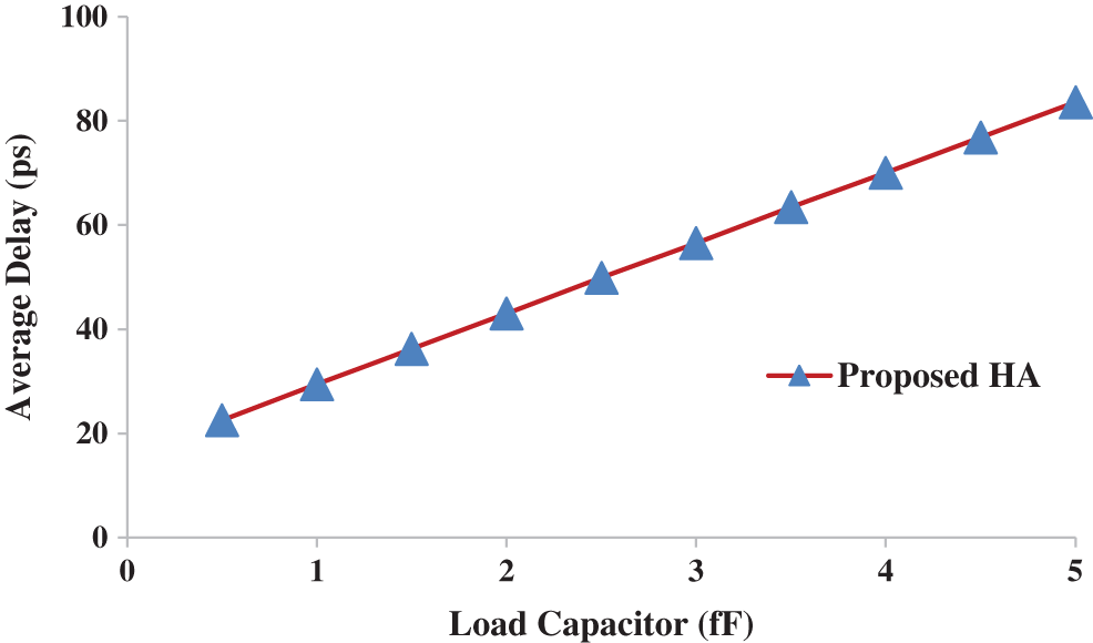
Figure 9: Load capacitance (fF) vs. average delay (ps)
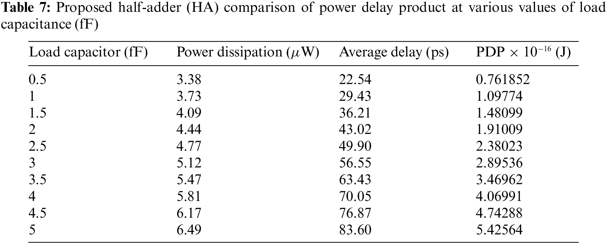
Fig. 10 shows the variation of power dissipation, measured in microwatts (µW), with load capacitance, measured in femtofarads (fF). From Fig. 10, it can easily be seen that if the load capacitance is maximized, the power dissipation is also maximized. The PDP values for various load capacitors is also analyzed and shown in Fig. 11. It is noticed that the PDP value is increased for higher load capacitor value.
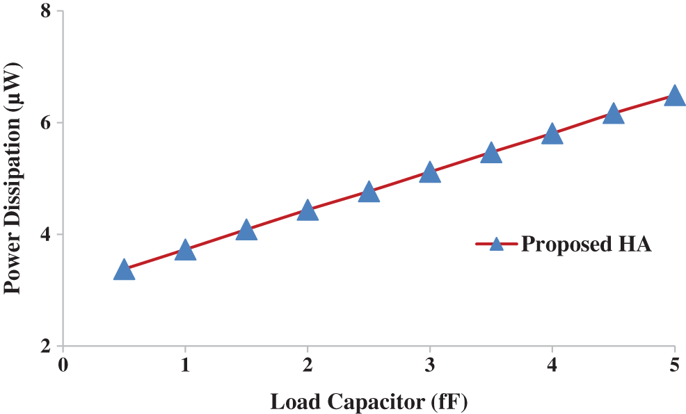
Figure 10: Load capacitance (fF) vs. power dissipation (µW)
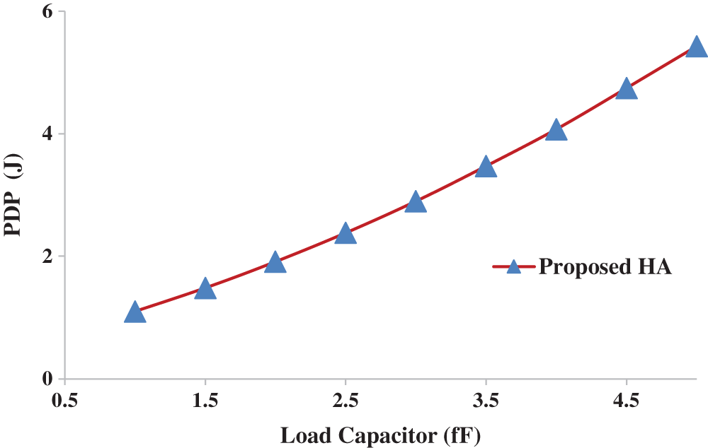
Figure 11: Load capacitance (fF) vs. power delay product × 10−16 (J)
Note: Power delay product is the product of power times delay.
Tab. 4 below shows that the performance of transistor count, voltage applied, delay, power, and power delay product (PDP) of the model design were all satisfactory. Furthermore, the comparison of various transition time delays, power dissipation and PDP for various load capacitor are given in Tabs. 5–7, respectively.
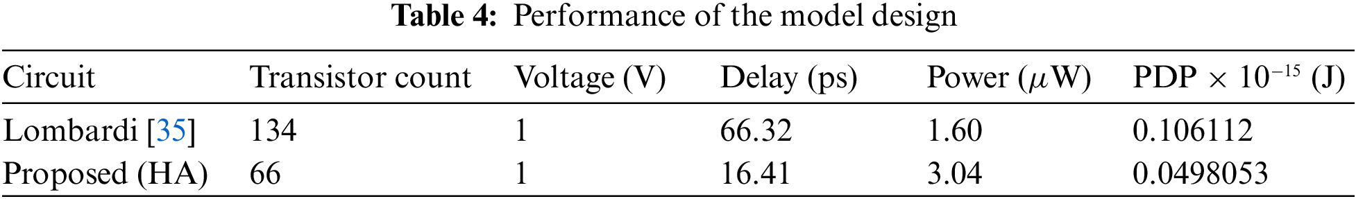

A novel three-input logic-based adder using CNTFETs is described in this paper. The major function of the adder is the lowering of the CNTFET threshold voltage, and a novel two-valued diameter (n, m) CNTFET-based three-input structure was designed for this purpose. Using the CNTFET paradigm, HSPICE was used to implement the proposed and previously stated designs, and was also used for the simulations [36]. Herein, the proposed design when compared to the existing design reduced the delay from 66.32 to 16.41 ps, i.e., a 75.26% reduction in delay; however, the power dissipation was not optimized, and was increased by 1.44% compared to the existing adder. The number of transistors was reduced and the product of power and delay (P*D) achieved a value of 0.0498053 fJ. An improvement at 1V was achieved, and we obtained a load capacitance (fF) measured at different values and an average delay with a maximum of 83.60 ps and a minimum of 22.54 ps, with a range of 61.06 ps. We also obtained different measurements of power dissipation, from a minimum of 3.38 µW to a maximum of 6.49 µW, measuring the power for different values of load capacitance, which represented the analyzed values of the proposed method. Based on these results, we can say that the use of this CNTFET half-adder design in multiple Boolean circuits is possible, and this adder design has been successfully used for the design and execution of complex circuits employed in CNTFET devices. The main limitation of this adder is that it uses more power than the existing model.
Funding Statement: The authors received no specific funding for this study.
Conflicts of Interest: The authors declare that they have no conflicts of interest to report regarding the present study.
References
1. M. Khaleqi Qaleh Jooq and M. Hossein Moaiyeri, “Ultra-compact ternary logic gates based on negative capacitance carbon nano tube FETs,” IEEE Transactions on Circuits and Systems I: Express Briefs, vol. 68, no. 6, pp. 2162–2166, 2021. [Google Scholar]
2. S. Heo, S. Kim, K. Kim, H. Lee, S. Kim et al., “Ternary full adder using multi-threshold voltage graphene barristors,” IEEE Electron Device Letters, vol. 39, no. 12, pp. 1948–1951, 2018. [Google Scholar]
3. A. Bachtold, P. Hadley, T. Nakanishi and C. Dekker, “Logic circuits with carbon nanotube transistors,” Science, vol. 294, no. 5545, pp. 1317–1320, 2001. [Google Scholar]
4. D. A. Rich, “A survey of multivalued memories,” IEEE Transactions on Computers, vol. 35, no. 2, pp. 99–106, 1986. [Google Scholar]
5. W. Huang, H. Zhu, Y. Zhang and Z. Wu, “A robust 3-D medical watermarking based on wavelet transform for data protection,” IEEE Transactions on Electron Devices, vol. 68, no. 7, pp. 3678–3683, 2021. [Google Scholar]
6. M. H. Moaiyeri, R. F. Mirzaee, A. Doostaregan, K. Navi and O. Hashemipour, “A universal method for designing low-power carbon nanotube FET-based multiple-valued logic circuits,” IET Computers & Digital Techniques, vol. 7, no. 4, pp. 167–181, 2013. [Google Scholar]
7. R. Saito, G. Dresselhaus and M. S. Dresselhaus,“ Carbon materials, tight binding calculation of molecules and solids, structure of a single wall carbon nano tube, electronic structure of single wall nano tube and synthesis of carbon nano tubes,” in Physical Properties of Carbon Nanotubes, vol. 35, Singapore: World Scientific, 1998. [Google Scholar]
8. H. Sirugudi, S. Gadgil and C. Vudadha, “A novel low power ternary multiplier design using CNFETS,” in 2020 33rd Int. Conf. on VLSI Design and 2020 19th Int. Conf. on Embedded Systems (VLSID), Banglore, India, pp. 25–30, 2020. [Google Scholar]
9. M. H. Ben-Jamaa, K. Mohanram and G. de Micheli, “An efficient gate library for bipolar CNTFET logic,” IEEE Transactions on Computer-Aided Design of Integrated Circuits and Systems, vol. 30, no. 2, pp. 242–255, 2011. [Google Scholar]
10. J. T. Butler and Y. -H. Chang, “The design of current-mode CMOS multiple-valued circuits,” in Proc. of 21st Int. Symp. on Multiple-Valued Logic, Victoria, BC, Canada, pp. 4054–4057, 1991. [Google Scholar]
11. A. Raychowdhury and K. Roy, “Carbon-nanotube-based voltage-mode multiple-valued logic design,” IEEE Transactions on Nanotechnology, vol. 4, no. 2, pp. 168–179, 2005. [Google Scholar]
12. I. O’Connor, J. Liu, F. Gaffiot, F. Prégaldiny, C. Lallement et al., “CNTFET modeling and reconfigurable logic-circuit design,” IEEE Transactions on Circuits and Systems I: Regular Papers, vol. 54, no. 11, pp. 2365–2379, 2007. [Google Scholar]
13. M. -H. Yangetal, K. B. K. Teo, L. Gangloff, W. L. Milne, D. G. Hasko et al., “Advantages of top-gate, high-k dielectric carbon nanotube field-effect transistors,” Applied Physics Letters, vol. 88, no. 11, Art. no. 113507, pp. 1–3, 2006. [Google Scholar]
14. Y. Lin, J. Appenzeller, J. Knoch and P. Avouris, “High-performance carbon nanotube field-effect transistor with tunable polarities,” IEEE Transactions on Nanotechnology, vol. 4, no. 5, pp. 481–489, 2005. [Google Scholar]
15. P. Avouris, J. Appenzeller, R. Martel and S. J. Wind, “Carbon nanotube electronics,” Proceedings of IEEE, vol. 91, no. 11, pp. 1772–1784, 2003. [Google Scholar]
16. G. S. Tulevski, A. D. Franklin, D. Frank, J. M. Lobez, Q. Cao et al., “Toward high-performance digital logic technology with carbon nanotubes,” ACS Nano, vol. 8, no. 9, pp. 8730–8745, 2014. [Google Scholar]
17. J. Guo, S. Hasan, A. Javey, G. Bosman and M. Lundstrom, “Assessment of high-frequency performance potential of carbon nanotube transistors,” IEEE Transactions on Nanotechnology, vol. 4, no. 6, pp. 715–721, 2005. [Google Scholar]
18. F. Lombardi, Y. -B. Kim and S. Lin, “Design of a ternary memory cell using CNTFET,” IEEE Transactions on Nanotechnology, vol. 11, no. 5, pp. 1019–1025, 2012. [Google Scholar]
19. S. Kim, S. -Y. Lee, S. Park, K. -R. Kim and S. Kang, “A logic synthesis methodology for low power ternary logic circuits,” IEEE Transactions On Circuits and Systems I: Regular Papers, vol. 67, no. 9, pp. 1–14, 2020. [Google Scholar]
20. R. Martel, T. Schmidt, H. Shea, T. Hertel and P. Avouris, “Single-and multi-wall carbon nanotube field-effect transistors,” Applied Physics Letters, vol. 73, no. 17, pp. 2447–2449, 1998. [Google Scholar]
21. S. Lin, Y. -B. Kim and F. Lombardi, “A novel CNTFET-based ternary logic gate design,” in Proc. of IEEE Int. Midwest Symp. on Circuits and Systems, Cancun, Mexico, pp. 435–438, 2009. [Google Scholar]
22. A. Raychowdhury and K. Roy, “Carbon-nanotube-based voltage-mode multiple-valued logic design,” IEEE Transactions on Nanotechnology, vol. 4, no. 2, pp. 168–179, 2005. [Google Scholar]
23. A. Dhande and V. Ingole, “Design and implementation of 2-bit ternary ALU slice,” in Proc. of Int. Conf. on IEEE-Science Electronic Technology Information & Telecommunication, Tunisia, vol. 13, pp. 17–21, 2005. [Google Scholar]
24. M. Mukaidono, “Regular ternary logic functions—Ternary logic functions suitable for treating ambiguity,” IEEE Transactions on Computers, vol. 35, no. 2, pp. 179–183, 1986. [Google Scholar]
25. Stanford University CNFET model website, Stanford University, Stanford, CA, 2008. [Online]. Available: http://nano.stanford.edu/model.php?id=23,. [Google Scholar]
26. A. Lin, N. Patil, K. Ryu, A. Badmaev, L. G. DeArco et al., “Threshold voltage and on-off ratio tuning for multiple-tube carbon nanotube FETs,” IEEE Transactions on Nanotechnology, vol. 8, no. 1, pp. 4–9, 2009. [Google Scholar]
27. Y. Ohno, S. Kishimoto, T. Mizutani, T. Okazaki and H. Shinohara, “Chirality assignment of individual single-walled carbon nanotubes in carbon nanotube field-effect transistors by micro-photocurrent spectroscopy,” Applied Physics Letters, vol. 84, no. 8, pp. 1368–1370, 2004. [Google Scholar]
28. X. R. Zhang, W. F. Zhang, W. Sun, X. M. Sun and S. K. Jha, “A robust 3-D medical watermarking based on wavelet transform for data protection,” Computer Systems Science & Engineering, vol. 41, no. 3, pp. 1043–1056, 2022. [Google Scholar]
29. X. R. Zhang, X. Sun, X. M. Sun, W. Sun and S. K. Jha, “Robust reversible audio watermarking scheme for telemedicine and privacy protection,” Computers, Materials & Continua, vol. 71, no. 2, pp. 3035–3050, 2022. [Google Scholar]
30. J. Deng and H. -S. P. Wong, “A compact SPICE model for carbon-nanotube field-effect transistors including nonidealities and its application. Part I: Model of the intrinsic channel region,” IEEE Transactions on Electron Devices, vol. 54, no. 12, pp. 3186–3194, 2007. [Google Scholar]
31. J. Deng and H. -S. P. Wong, “A circuit-compatible SPICE model for enhancement mode carbon nanotube field effect transistors,” in Proc. of Int. Conf. on Simulation of Semiconductor Processes and Devices, Monterey, CA, USA, pp. 166–169, 2006. [Google Scholar]
32. S. Subhendu Kumar, G. Akhilesh, S. Rasmita and M. Manasi, “High-performance ternary adder using CNTFET,” IEEE Transactions on Nanotechnology, vol. 16, no. 3, pp. 368–374, 2017. [Google Scholar]
33. J. Deng and H. -S. P. Wong, “A compact SPICE model for carbon-nanotube field-effect transistors including nonidealities and its application. Part II: Full device model and circuit performance benchmarking,” IEEE Transactions on Electron Devices, vol. 54, no. 12, pp. 3195–3205, 2007. [Google Scholar]
34. C. P. Bhargavi, G. Ramachandra Kumar and P. Sireesha, “A study on various approaches in designing ternary half adder,” in IEEE Int. Conf. on Computer Communication and Informatics, Coimbatore, India, vol. 5, pp. 1–9, 2021. [Google Scholar]
35. S. Lin, Y. -B. Kim and F. Lombardi, “CNTFET-based design of ternary logic gates and arithmetic circuits,” IEEE Transactions on Nanotechnology, vol. 10, no. 2, pp. 217–225, 2011. [Google Scholar]
36. J. Deng and H. -S. P. Wong, “Modeling and analysis of planar-gate electrostatic capacitance of 1-D FET with multiple cylindrical conducting channels,” IEEE Transactions on Electron Devices, Coimbatore, India, vol. 54, no. 9, pp. 2377–2385, 2007. [Google Scholar]
 | This work is licensed under a Creative Commons Attribution 4.0 International License, which permits unrestricted use, distribution, and reproduction in any medium, provided the original work is properly cited. |