| Computers, Materials & Continua DOI:10.32604/cmc.2022.029049 | |
| Article |
Multi-Band Bandpass Filter Using Novel Topology for Next-Generation IoT Wireless Systems
Departmnet of Electrical Engineering, Riphah International University, Islamabad, 44000, Pakistan
*Corresponding Author: Muhammad Faisal. Email: muhammad.faisal@riphah.edu.pk
Received: 24 February 2022; Accepted: 17 May 2022
Abstract: The design of single- and quad-band Bandpass Filter (BPF) topology has been presented in this paper for next-generation Internet of Things (IoT) devices. The main topology is constructed using the Split Ring Resonator (SRR), separated by the Anti-Parallel Coupled Line Structure (APCLS). A detailed analysis of APCLS has been presented, which is further used to construct the single- and quad-band BPF. The single-band BPF design consists of SRR loaded with APCLS. The developed single-band BPF displays a dual-mode response with a center frequency of 2.65 GHz and a measured fractional bandwidth of 17.17%. Moreover, a quad-band bandpass filter has been achieved using the same topology with minor modification in the SRR and APCLS electrical parameters. The developed quad-band BPF generates a dual-mode response having center frequencies of 1.2, 2.4, 3.5, and 4.7 GHz with the measured fractional bandwidth of 13%, 26%, 16%, and 5%, respectively. Two prototypes have been fabricated on the high-frequency substrate to validate the proposed topologies. Very high rejection in the stopbands region, little in-band insertion loss, and very selective passband have been measured for single- and quad-band BPFs. The measured and simulated results are well correlated.
Keywords: Single-band BPF; quad-band BPF; anti-parallel coupled line structure; split ring resonator; internet of things
Modern IoT wireless communication systems, like Bluetooth, Zonal Intercommunication Global-standard (ZigBee), Long Range Radio (LoRa), NarrowBand (NB)-IoT, and Wireless Fidelity (WiFi) demand multiband frequency response. Moreover, the IoT wireless communication nodes required low-powered miniaturized designed components. Therefore, the RF front end of an IoT device must have a compact design while maintaining good electrical performance. Over the last few years, many researchers have provided the design topologies of single and multiband BPF for low-powered compact IoT devices. In [1], the proposed structure involves two sections of three-quarter wavelength coupled lines separated by a non-uniform transmission line to obtain a wideband BPF filter response. Moreover, a dual-path structure that involves an inter-digital coupled line in parallel with the transmission line is presented in [2] to realize a wide BPF response. Another coupled step impedance resonator (SIR) technique in [3] is used to realize the single and dual-band BPF response. The measured result shows little discrepancies at the upper stopband for both single and dual BPF filters. Furthermore, three pairs of coupled lines structures and two pairs of transmission lines are integrated in such a way to obtain a highly selective BPF response [4]. The ideal response consists of eight transmission zeros (TZs) and five transmission poles (TPs) within the 2fc; however, the microstrip and fabricated results show less TZs at the upper stopband. The cross-shaped resonator having three coupled line structures is integrated to achieve the wide BPF filter response [5]. The resonator having a parallel-coupled line as feed is replaced with three coupled line feed to achieve strong coupling that helped in obtaining better out of band rejection and reducing the return loss in the passband.
The wide BPF response using the ring embedded ring resonator technique is realized in [6]. The embedded rings helped reduce the size of the filter and produce a wider upper stopband. However, the measured result shows high discrepancies in the upper stopband region compared to the simulated results. The structure having two coupled SIR and a ring resonator in the ground plane is implemented to achieve a better wide BSF response [7]. The presence of the ring resonator in the ground plane enhanced the coupling of the overall structure and extracted a better passband response. The Stub-loaded Square ring resonator technique achieves single and dual-band BPF response [8]. A single BPF response is obtained by implementing a simple stub-loaded square ring resonator separated by an interdigital coupled line feed. Whereas the dual BPF response is achieved using two stub-loaded square ring resonators in the overall structure separated through coupled feeds. The measured result for the dual-band BPF filter shows high discrepancies in the upper passband compared to the simulated result.
Over the last decade, multi-band BPFs have gained popularity in multi-band IoT wireless communication systems. Substantial research has been done on dual- and tri-band BPFs. Nowadays, researchers are more focused on developing miniaturized quad-, penta-, and sext-band BPFs. Different design topologies have been adopted to develop quad-band BPF [9–23]. A popular method to design a quad-band BPF is by using stub-loaded topology [9–13]. In [9], a quad-band BPF with only three finite frequency transmission zeros using symmetrical stub-loaded topology has been presented. The two upper passbands measured insertion loss is not up to the mark. Two open-ended stubs resonators are loaded at the center of the two outer resonators [10] to achieve a quad-band BPF response. High discrepancies between the simulated and measured results have been noted for the upper passbands. A multi-stub-loaded resonator is presented in [11] to obtain a quad-band BPF response. Different stubs configurations can independently control the frequencies. However, each band's insertion loss and selectivity are not good enough. In [12], another quad-band BPF has been presented using a stub-loaded resonator. The even and odd mode method is used to analyze the symmetrical structure. However, the insertion loss is very high for each passband; moreover, the return loss is not up to the mark. Additionally, the quad-band BPF response has been realized using the multi-section stub-loaded resonators [13]. Five transmission zeros have been obtained around the passband to enhance the selectivity, whereas the insertion loss is quite high for each passband. Moreover, the SIR topology has been utilized to obtain quad-band BPF response [14,15,20]. In [14], open-circuited SIR loaded with short-circuited stubs is utilized to realize the quad-band BPF response with three transmission zeros across the four passbands. The overall size of the circuit is compact, but the insertion loss is above 2.3 dB. A triangular loop open-circuited stub-loaded SIR is implemented to achieve a quad-band BPF response [20]. The return loss is quite better, having six transmission zeros for better selectivity and isolation, but the insertion loss is bad. Moreover, the step impedance ring resonator (SIRR) topology is reported in [21] to obtain quad-band BPFs. The input/output coupled line structure is implemented with the SIRR to generate four passbands. However, the insertion loss in the upper three passbands is quite high.
In this paper, the single- and quad-band BPF is designed using the SRR loaded with the APCLS. At first, the single-band BPF is designed using the proposed topology; afterward, little modification in the electrical parameters of the topology is performed to obtain the quad-band BPF response. The accomplished single- and quad-band BPF provides a dual-mode response with good electrical performance having higher out-of-band rejection and selectivity. A total of three and seven finite frequency transmission zeros are achieved for single and quad-band BPF filters, respectively. The finite frequency transmission zeros and the band of both the filters can be controlled through the variation in the dimensions of the SRR and APCLS. The prototypes are fabricated on RT/Duroid 5880 with a relative dielectric constant of 2.2. The selected substrate is low-powered and rugged, providing a suitable integration in a wireless IoT node RF front end. The measured results show good agreement with the simulated results for both filters.
Fig. 1 displays the ideal topology of the proposed single- and quad-band BPF. The topology consists of a split ring resonator separated through the anti-parallel coupled line structure.
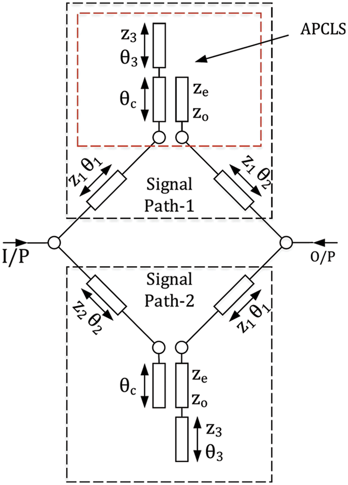
Figure 1: Ideal topology of SRR loaded with APCLS
Four transmission lines that are part of SRR have the characteristic impedance of
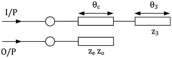
Figure 2: Proposed anti-parallel coupled line structure
2.1 Proposed Anti-parallel Coupled Line Structure
The APCLS is developed using the parallel-coupled line with the even and odd impedances
In [24], the transfer matrix of the parallel-coupled line structure has already been discussed and concluded in the form of equations Eqs. (1) and (2).
An extra load at port 3 of the parallel-coupled line structure can be expressed in the form of an open-circuited stub as given in Eq. (3).
The electrical length
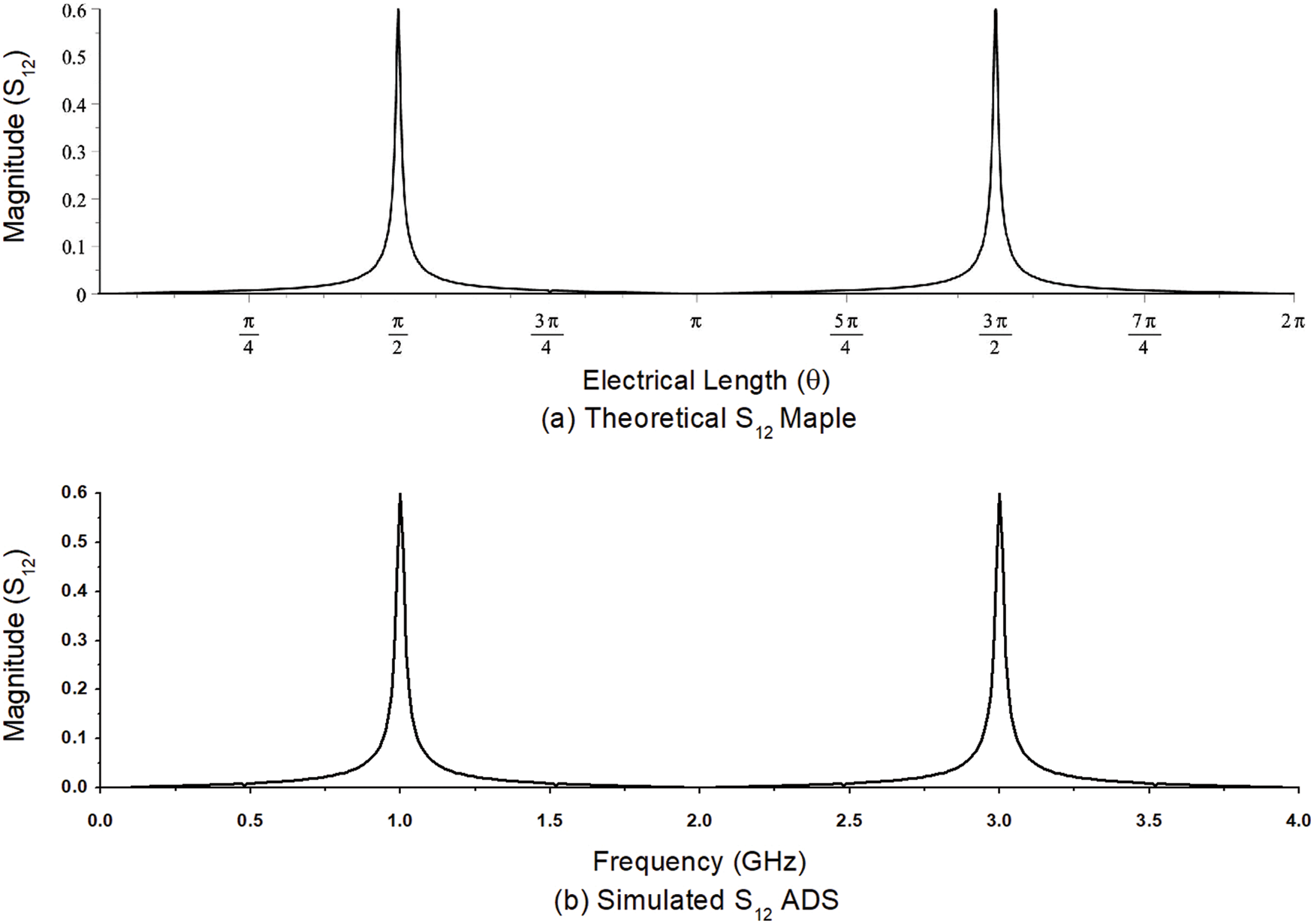
Figure 3: Comparison of theoretical and simulated response of APCLS
where,
2.2 Proposed Single-Band BPF Filter
The proposed single-band BPF filter is constructed using the SRR loaded with the APCLS. The transfer matrix of the anti-parallel coupled line structure is already being extracted. It can be observed from Fig. 1 that the path 1 and path 2 are in parallel; therefore, the extracted transfer matrix of path 1, and path 2 is converted into their respective admittance matrix. The addition is performed on the admittance matrix of both paths to calculate the final admittance matrix. Afterward, the final admittance matrix is converted back into the transfer matrix to calculate the scattering parameter given in Eq. (5). To avoid complexity the impedances
where,
The values of
By using the synthesis procedure opted in [25,26], the coefficient values are extracted. Furthermore, the electrical parameters of the single-band bandpass filter shown in Fig. 4 are calculated using the coefficient values. The obtained electrical parameter values are

Figure 4: Ideal design of the proposed single-band BPF

Figure 5: Ideal response of the proposed single-band BPF
Through detailed analysis, it has been observed that the finite frequency transmission zeros are controlled by the electrical length of SRR and APCLS. To provide the evidence, Fig. 6 shows the tuning of transmission zeros. Fig. 6a reveals that by increasing the electrical length

Figure 6: Simulated results with tuning the electrical length
Similarly, with the variation in the electrical length
2.3 Proposed Quad-Band BPF Filter
The proposed quad-band BPF utilizes the same topology as of single-band BPF shown in Fig. 5; however, little modification in the electrical parameters of SRR and APCLS has been realized to obtain the dual-mode quad-band BPF response. Simulated results with tuning the electrical length
The extracted coefficient values are used to obtain the electrical parameters of the quad-band BPF. The obtained electrical parameter values are

Figure 7: Ideal response of the proposed quad-band BPF
In order to further analyze the design topology, different electrical parameters are tuned, and the corresponding results are shown in Fig. 8. By changing the electrical length
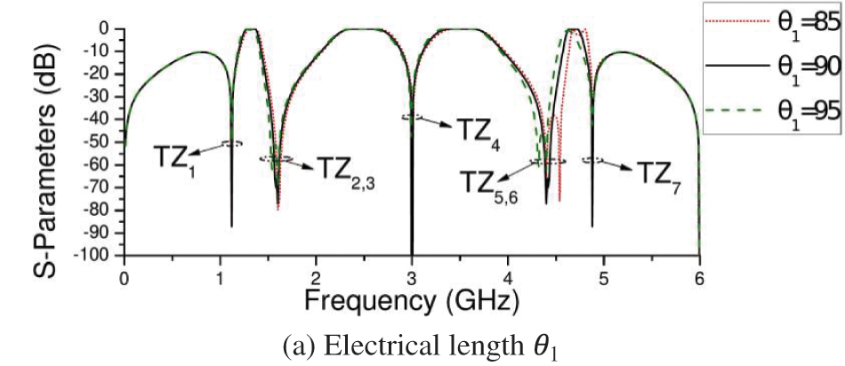
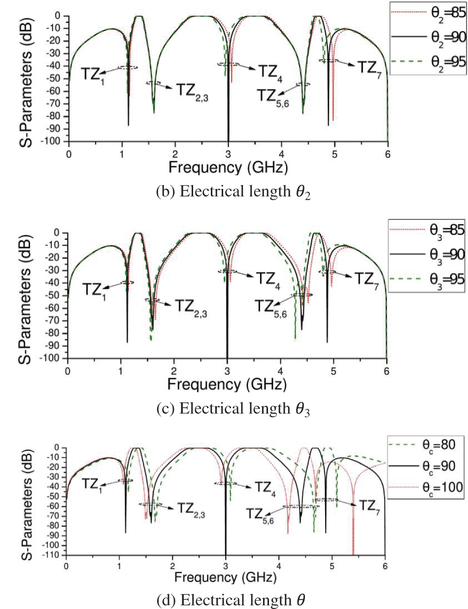
Figure 8: Simulated results with tuning the electrical length
For validation, the proposed single and quad-band BPF topologies are fabricated on Rogers Duroid 5880, and the measurements are done on Agilent N5242A PNA-X. The electrical parameters of both BPF filters are converted into their respective physical parameters using a line calculator, and the losses have been minimized using full-wave EM simulation.
The single-band BPF shown in Fig. 9 is labeled with optimized physical parameters at 2.65 GHz center frequency. The optimized physical parameters are

Figure 9: Top view of the single-band BPF filter
Two transmission poles are measured at 2.48 GHz, and 2.68 GHz, as shown in Fig. 10. The 3 dB fractional bandwidth is measured to be 17.7

Figure 10: Simulated and measured results of fabricated single-band BPF

Figure 11: Measured group delay
The optimized electrical parameters of quad-band BPF filters is converted to physical parameters using a line calculator. The tuning and optimization is done to minimise the substrate losses. The optimized physical parameters labeled in Fig. 12 are
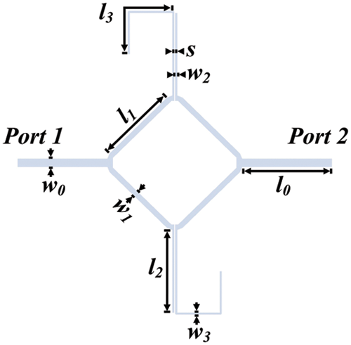
Figure 12: Top view of quad-band BPF
The comparison of microstrip simulated and measured results are shown in Fig. 13. Four passbands are measured, having center frequencies at 1.2 GHz, 2.4 GHz, 3.5 GHz, and 4.7 GHz, respectively. The 3 dB fractional bandwidth is measured to be 13

Figure 13: Measured and simulated results comparison

Figure 14: Measured group delay
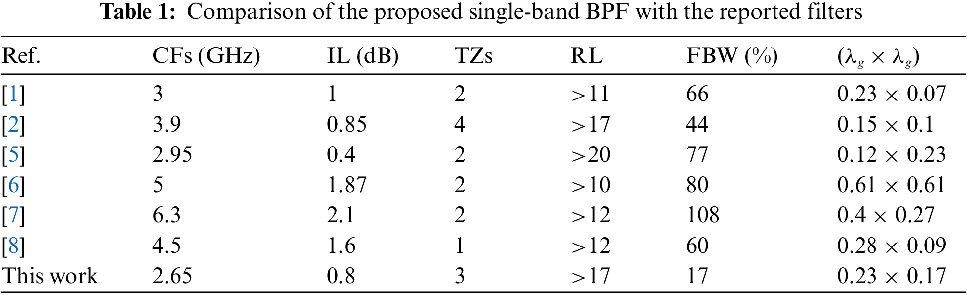
Tab. 1 illustrates the comparison of the proposed single-band BPF with the previously reported work in the literature.
Tab. 2 shows the comparison of the proposed quad-band BPF with the reported ones. It can be seen from the table that the proposed filter provides better selectivity, low insertion loss, low to high fractional bandwidth, and higher out of band rejection.

A split-ring resonator separated by an anti-parallel coupled line structure topology has been proposed to achieve single- and quad-band BPF. The synthesis procedure has been adopted to obtain the electrical parameters of the single and quad-band BPF. Moreover, the theory of the proposed topologies has been validated through the measured results of the fabricated prototypes. The calculated results of single- and quad-band BPF shows very low insertion loss in the passband and very high rejection in the lower and upper stopband regions. The proposed structures are suitable candidates for next-generation IoT wireless communication devices.
Acknowledgement: The authors would like to thanks the editors and reviewers for their review and recommendations.
Funding Statement: The authors received no specific funding for this study.
Conflicts of Interest: The authors declare that they have no conflicts of interest to report regarding the present work.
References
1. H. N. Shaman, “New S-band bandpass filter BPF with wideband passband for wireless communication systems,” IEEE Microwave and Wireless Components Letters, vol. 22, no. 5, pp. 242–244, 2012. [Google Scholar]
2. K. Tanii and K. Wada, “Wideband bandpass filter composed of dual-path resonators using coupled-line and transmission line with inductive elements,” IEEE Microwave and Wireless Components Letters, vol. 24, no. 1, pp. 14–16, 2013. [Google Scholar]
3. H. Zhu and A. M. Abbosh, “Single-and dual-band bandpass filters using coupled stepped-impedance resonators with embedded coupled-lines,” IEEE Microwave and Wireless Components Letters, vol. 26, no. 9, pp. 675–677, 2016. [Google Scholar]
4. C. J. Chen, “A coupled-line coupling structure for the design of quasi-elliptic bandpass filters,” IEEE Transactions on Microwave Theory and Techniques, vol. 66, no. 4, pp. 1921–1925, 2018. [Google Scholar]
5. D. S. La, X. Guan, S. M. Chen, Y. Y. Li and J. W. Guo, “Wideband band-pass filter design using coupled line cross-shaped resonator,” MDPI Electronics, vol. 9, no. 12, pp. 2173, 2020. [Google Scholar]
6. A. Nakhlestani and A. Hakimi, “Wideband microstrip ring resonator bandpass filter with embedded rings,” Microelectronics Journal, vol. 44, no. 5, pp. 462–467, 2013. [Google Scholar]
7. D. Sarkar, T. Moyra and L. Murmu, “An ultra-wideband (UWB) bandpass filter with complementary split ring resonator for coupling improvement,” AEU-International Journal of Electronics and Communications, vol. 71, no. 11, pp. 89–95, 2017. [Google Scholar]
8. P. Zhang, L. Liu, D. Chen, M. H. Weng and R. Y. Yang, “Application of a stub-loaded square ring resonator for wideband bandpass filter design,” MDPI Electronics, vol. 9, no. 1, pp. 176, 2020. [Google Scholar]
9. J. Y. Wu and W. H. Tu, “Design of quad-band bandpass filter with multiple transmission zeros,” IET Electronics letters, vol. 47, no. 8, pp. 502–503, 2011. [Google Scholar]
10. B. Wu, F. Qiu and L. Lin, “Quad-band filter with high skirt selectivity using stub-loaded nested dual-open loop resonators,” IET Electronics Letters, vol. 51, no. 2, pp. 166–168, 2015. [Google Scholar]
11. L. Gao, X. Y. Zhang, X. L. Zhao, Y. Zhang and J. X. Xu, “Novel compact quad-band bandpass filter with controllable frequencies and bandwidths,” IEEE Microwave and Wireless Components Letters, vol. 26, no. 6, pp. 395–397, 2016. [Google Scholar]
12. L. Murmu and S. Das, “A compact quad-band bandpass filter using multi-mode stub-loaded resonator,” Progress In Electromagnetics Research Letters, vol. 61, pp. 39–46, 2016. [Google Scholar]
13. Q. Cao, H. Liu and L. Gao, “Design of novel compact quad-band bandpass filter with high selectivity,” De Gruyter Frequenz, vol. 74, no. 1–2, pp. 53–59, 2020. [Google Scholar]
14. J. Xu, C. Miao, L. Cui, Y. X. Ji and W. Wu, “Compact high isolation quad-band bandpass filter using quad-mode resonator,” IET Electronics Letters, vol. 48, no. 1, pp. 28–30, 2012. [Google Scholar]
15. X. Li, Y. Zhang, Y. Tian, Y. Yang and Y. Fan, “Quad-and sext-band bandpass filter based on multimode resonator utilizing SIRs-loaded tapered-line,” Microwave and Optical Technology Letter, vol. 60, no. 3, pp. 650–654, 2018. [Google Scholar]
16. Q. Yang, Y. C. Jiao and Z. Zhang, “Compact multiband bandpass filter using low-pass filter combined with open stub-loaded shorted stub,” IEEE Transactions on Microwave Theory and Techniques, vol. 66, no. 4, pp. 1926–1938, 2018. [Google Scholar]
17. Z. Li, L. Wang, M. He, X. Li, Z. Liang et al., “Compact dual-/tri-/quad-band bandpass filters with independently frequency-tunable and switchable passbands,” International Journal of Microwave and Wireless Technologies, vol. 13, no. 4, pp. 322–334, 2021. [Google Scholar]
18. D. K. Choudhary and R. K. Chaudhary, “Miniaturized quad-band filter with improved selectivity using split ring resonators and metallic strips,” International Journal of RF and Microwave Computer-Aided Engineering, vol. 31, no. 10, pp. e22809, 2021. [Google Scholar]
19. J. Zhang, Q. Liu, D. W. Zhang and Y. Qu, “High selectivity single wideband and quad-band HTS filters using novel quad-mode resonators with self-coupled structure,” IEEE Access, vol. 9, pp. 103194–103203, 2021. [Google Scholar]
20. J. Wang, S. He and D. Gan, “A 2.4/3.5/5.2/5.8-GHz quad-band BPF using SLRs and triangular loop resonators,” IET Electronics Letters, vol. 54, no. 5, pp. 299–301, 2018. [Google Scholar]
21. F. Wei, Q. Huang, X. H. Wang, W. T. Li and X. W. Shi, “Compact step-impedance ring resonator for quad-band band-pass filter,” Progress In Electromagnetics Research Letters, vol. 41, pp. 105–112, 2013. [Google Scholar]
22. X. R. Zhang, X. Sun, W. Sun, T. Xu and P. P. Wang, “Deformation expression of soft tissue based on BP neural network,” Intelligent Automation & Soft Computing, vol. 32, no. 2, pp. 1041–1053, 2022. [Google Scholar]
23. J. Zhang, Z. Wang, Y. Zheng and G. Zhang, “Design of network cascade structure for image super-resolution,” Journal of New Media, vol. 3, no. 1, pp. 29–39, 2021. [Google Scholar]
24. G. I. Zysman and A. K. Johnson, “Coupled transmission line networks in an inhomogeneous dielectric medium,” IEEE Transactions on Microwave Theory and Techniques, vol. 17, no. 10, pp. 753–759, 1969. [Google Scholar]
25. S. Khalid, W. Peng Wen and L. Yen Cheong, “Optimum filter synthesis procedure for ultra-wideband bandpass filter using step-impedance resonator,” Journal of Electromagnetic Waves and Applications, vol. 28, no. 8, pp. 943–955, 2014. [Google Scholar]
26. M. Faisal, S. Khalid, M. U. Rehman and M. A. Rehman, “Synthesis and design of highly selective multi-mode dual-band bandstop filter,” IEEE Access, vol. 9, pp. 43316–43323, 2021. [Google Scholar]
 | This work is licensed under a Creative Commons Attribution 4.0 International License, which permits unrestricted use, distribution, and reproduction in any medium, provided the original work is properly cited. |