DOI:10.32604/csse.2022.019449
| Computer Systems Science & Engineering DOI:10.32604/csse.2022.019449 | |
| Article |
Hardware Chip Performance of CORDIC Based OFDM Transceiver for Wireless Communication
1Faculty of Technology, Uttarakhand Technical University, Dehradun, 248007, India
2Department of Electrical & Electronics Engineering, School of Engineering, University of Petroleum and Energy Studies, Dehradun, 248007, India
3Birla Institute of Applied Sciences, Nainital, 263136, India
*Corresponding Author: Adesh Kumar. Email: adeshmanav@gmail.com
Received: 13 April 2021; Accepted: 14 May 2021
Abstract: The fourth-generation (4G) and fifth-generation (5G) wireless communication systems use the orthogonal frequency division multiplexing (OFDM) modulation techniques and subcarrier allocations. The OFDM modulator and demodulator have inverse fast Fourier transform (IFFT) and fast Fourier transform (FFT) respectively. The biggest challenge in IFFT/FFT processor is the computation of imaginary and real values. CORDIC has been proved one of the best rotation algorithms for logarithmic, trigonometric, and complex calculations. The proposed work focuses on the OFDM transceiver hardware chip implementation, in which 8-point to 1024-point IFFT and FFT are used to compute the operations in transmitter and receiver respectively. The coordinate rotation digital computer (CORDIC) algorithm has read-only memory (ROM)-based architecture to store FFT twiddle factors and their angle generators. The address generation unit is required to fetch the data and write the results into the memory in the appropriate sequence. CORDIC provides low memory, delay, and optimized hardware on the field-programmable gate array (FPGA) in comparison to normal FFT architecture for the OFDM system. The comparative performance of the FFT and CORDIC-FFT based OFDM transceiver chip is estimated using FPGA parameters: slices, flip-flops, lookup table (LUTs), frequency, power, and delay. The design is developed using integrated synthesis environment (ISE) Xilinx version 14.7 software, synthesized using very-high-speed integrated circuit hardware description language (VHDL), and tested on Virtex-5 FPGA.
Keywords: 5G Communication; CORDIC Algorithm; FFT; Virtex-5 FPGA; OFDM Communication
OFDM [1] is a multicarrier modulation technique used to modulate multiple carriers over a channel. It divides the input data stream into several parallel data streams. These streams are used to modulate multiple carriers and divide the available spectrum. OFDM efficiently uses spectrum by proving the space in the channels, closer to each other. The multiple carriers are orthogonal to each other and eliminate the problem of interference. There are several advantages of multicarrier modulation techniques in wireless communication such as delay spread tolerance, and spectral efficiency. In the OFDM technique, multiple carriers share the data among each other due to its orthogonal nature available in the spectrum band. The OFDM transmission technology has gained popularity in the broadband community due to its robust behavior against fading caused by multipath propagation [2]. The block diagram of the OFDM transceiver [3] is shown in Fig. 1. In the OFDM transmitter, the set of symbols as input streams are loaded serially. The input serial data stream is converted to a parallel data stream to load the number of symbols onto ‘N’ subcarriers using the de-multiplexing technique. The Institute of Electrical and Electronics Engineers (IEEE) standard wireless local area network (WLAN)-54 megabit per second (Mbps) is applied to map the data for complex symbols based on 64-quadrature amplitude modulation (QAM) modulation. The 64-QAM uses 6-bit per symbol. The QAM mapping is based on the constellation diagram in which the adjacent symbols in the transmitter should not vary more than 1-bit. It is achieved by changing the input symbols to gray coded symbols and then mapping to the preferred QAM constellation [4].
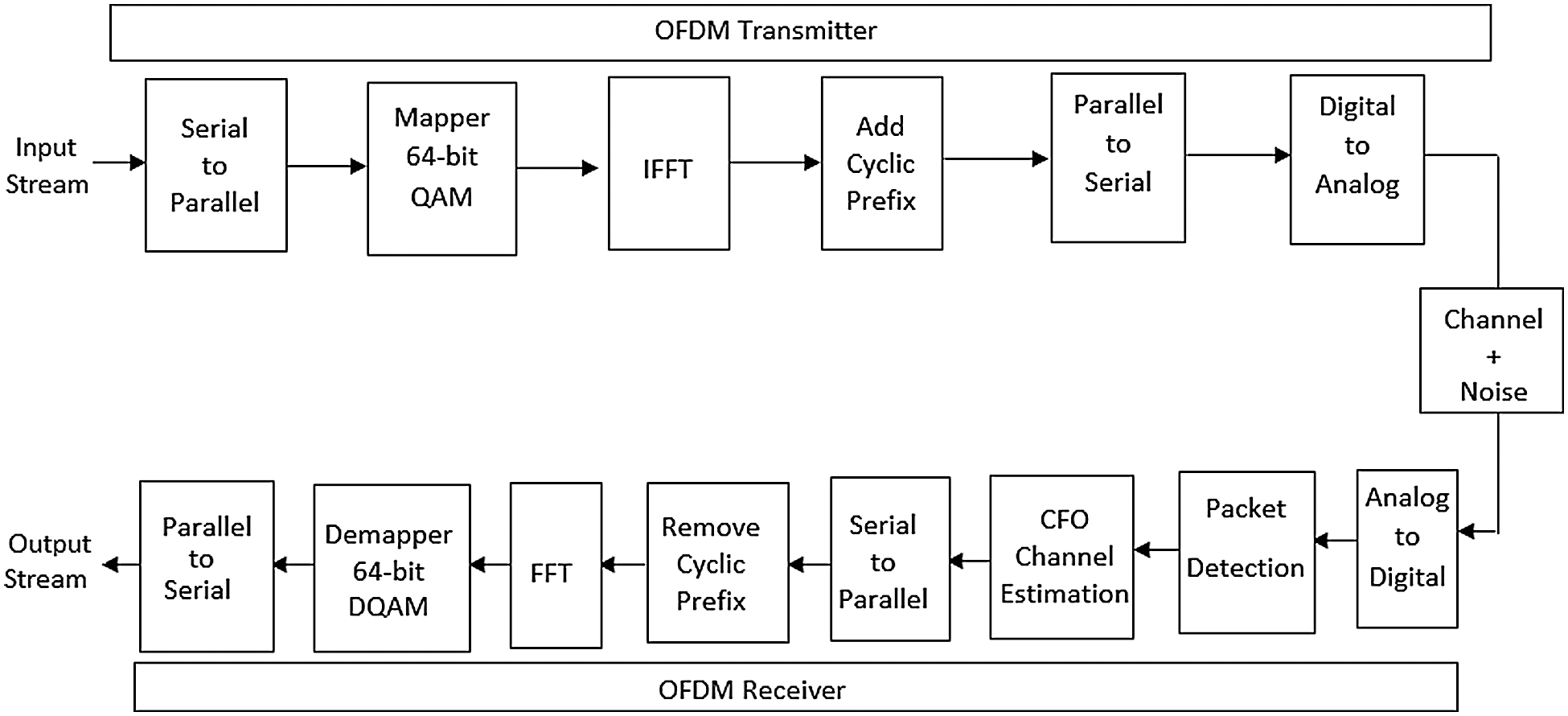
Figure 1: OFDM block diagram
The ‘N’ point IFFT is applied on subcarriers symbols. The IFFT generates the transmitted samples. The IFFT output is passed to parallel to the serial converter, also known as the multiplexing operation to generate the serial stream. The cyclic prefix [5], as guard band is added to the serial stream to avoid inter-block interference. The digital to analog converter (DAC) converts the data in digital form to data in an analog form which is transmitted over the additive white Gaussian noise (AWGN) channel. It presents the complete description of the transmitter section. In the receiver section, the receiver takes the samples from the channel and converted them into a digital signal with the help of an analog to digital converter (ADC).
In the cyclic prefix, the samples are affected by inter-block interference (IBI). Therefore, it is required to remove the output corresponding to the cycle prefix. The output is given to serial to parallel converter or de-multiplexer. The output of the de-multiplexer is given to the ‘N’ point FFT block. The FFT has the received samples after the cyclic prefix and its transformation provides the output against subcarriers. The size of IFFT and FFT [6] is variable, varies from 8-point to 1024-point. After removing the cyclic prefix of a specific length, the signal at the receiver end is decomposed into multiple subcarriers using discrete Fourier transform (DFT). After this subcarriers are multiplied to the inverse of frequency response. It equalizes the gain of the desired signal. The FFT output is given to the de-mapper at the sample detection section. The detected samples are following parallel to serial conversion using a multiplexer. Afterward, the multiplexed output is converted back to the serial stream, generated from the receiver section of OFDM. In the baseband receiver design, the behavior of the receiver is affected by the non-ideality and noise in the channel [7]. The radiofrequency (RF) is also considered along with sampling clock offset, carrier frequency offset (CFO), power amplifier design, in-phase/quadrature (I-Q) imbalance, and phase noise. The radiofrequency hardware design with ideal frequency is difficult to design, such as oscillator phase noise and power amplifier non-linearity. The CFO synchronization occurs when the local oscillator signal for down-conversion in the receiver section is not synchronized with the carrier signal confined in the received signal. The phenomenon is experienced based on two important factors: firstly, Doppler effects due to the movement of transmitter & receiver secondly, a frequency mismatch [8] in the OFDM transmitter and receiver. In OFDM the orthogonality and the behavior of carrier mismatch can result from inter-carrier interference (ICI) [9].
FFT is the core component of the OFDM system. The 2000/4000/8000-points FFT [10] was used for the CORDIC-based OFDM system. CORDIC architecture was used for channel state information (CSI) for the OFDM system [11]. The CORDIC algorithm hardware [12] architecture was designed for the OFDM receiver. The hardware was based on the CORDIC algorithm to get FFT to twiddle factor values. CORDIC-based OFDM architecture provides the platform for concurrent execution with time as well as frequency offset estimation in OFDM data packet delivery. CORDIC algorithm was used for synchronization of CFO [13] in OFDM receiver. The hardware architecture is implemented in FPGA and compact CORDIC provided the optimized results in terms of FPGA resource utilization and latency. The CORDIC algorithm was used to generate a rotation sequence [14] with lookup tables of small size based on synthesized pipelined FFT works at the speed of 222 megahertz (MHz). The memory-based 8192-point FFT was used for pipelined architecture [15] for OFDM. The design provided the best results in terms of space utilization, cost reduction, and delay on 2.04 mm chip area and frequency support of 198 MHz. An innovative 128-point based radix-24 FFT/IFFT architecture [16] was used for the OFDM system for complex multiplications. CORDIC algorithm was used for WLAN [17] based OFDM. They suggested that the OFDM receiver section can be processed with the help of the CORDIC algorithm-based FFT and save the hardware resources on FPGA. The hardware implementation of a CORDIC processor was done [18] for OFDM applications. The design was based on VHDL and synthesized on the Xilinx Spartan-3A FPGA kit. The Xilinx ISE synthesis tool was used to configure the design for XC3S200–4ft256. The CORDIC algorithm was used for residual frequency offset (RFO) [19] for OFDM communication. The hardware implementation has proved that the results are significant and achievable for low complexity. The detailed architecture of the rotational CORDIC algorithm was proposed [20,21] for digital signal processing (DSP) applications, software-defined radio, biomedical signal processing, neural networks, and multiple-input-multiple-output (MIMO) systems. A high-speed 128 to 8192-point FFT processor using a split radix FFT [22] was implemented OFDM systems for optimal power and area. The very large scale of integration (VLSI) architecture of CORDIC for the pipelined FFT [23] processor was designed using Verilog hardware description language (HDL) on 130 nanometers (nm) technology and compared Spartan-2, Spartan-3E, and Virtex-2 Pro FPGA. CORDIC integrated WLAN receiver [24] was designed for OFDM in Xilinx ISE and analyzed in Matrix Laboratory (MATLAB) simulation environment. The CORDIC algorithm was used to generate the angle coefficients for FFT computations to get the precise values. A low power, reduced memory-based CORDIC architecture [25] was designed for faster computations of FFT. The suggested algorithm occupies the ROM space based on the angle generation and new address allocation for the specified ROM memory. The radix-2 and 4 FFT are used for FPGA implementation. The synthesized results and theoretical results are matched. The observation predicts that CORDIC FFT uses 20% less memory utilization and 15% less power consumption in comparison to normal FFT operation. CORDIC-based OFDM system [26] was implemented in which pipelined data was processed for the optimal solution in terms of area and speed. The OFDM is a viable method for efficient bandwidth and high data rate in wireless communication. (I-Q) imbalance [27] and insufficient cyclic prefixes can degrade the performance of the OFDM system, result interblock interference (IBI) especially for MIMO-OFDM in doubly selective channels. The hardware chip designed for the FFT processor [28] was used for the OFDM transceiver system. The chip design is compiled in Xilinx 14.2 using VHDL and synthesized on Virtex-5 FPGA to estimate hardware as well as timing parameters. The CORDIC-based OFDM baseband receiver was utilized for the gain adjustment, initial gain/phase estimation, and phase compensation. The FFT processor was designed for MIMO-OFDM [29] and synthesized on the Altera cyclone II DE2 board for full support in real-time communication with pipelined architecture. The system performance is estimated based on Radix 2-multi-path delay commutator (MDC) based FFT, radix 2, and radix 4-FFT from a hardware utilization point of views such as slices, LUTs, and power. Radix 2-MDC FFT algorithm consumes less power, slices, and LUT for the targeted FPGA. The OFDM hardware chip implementation was done on Virtex-5 FPGA [30]. The CORDIC algorithm provides the precise values of sine and cosine angles in the system. The radix 2 FFT algorithm was implemented on Virtex-7 FPGA [31] based on decimal in frequency algorithm and FFT intellectual property (IP) core in Xilinx software. The design is optimized based on hardware resource utilization, speed, throughput, latency, and accuracy, of computation on an FPGA device. The CORDIC method was synthesized on the FPGA hardware for online learning of CORDIC Izhikevich neurons [32] to validate the competitive Hebbian-based learning. The cascaded CORDIC [33] was used to meet the time and area constraints in hardware design. They discussed the design of hybrid cascaded-recursive CORDIC. The design utilized 31.1% less area in comparison to fully pipelined CORDIC.
The OFDM is a type of digital transmission that encodes digital data onto multiple carrier frequencies. There are several platforms to realize the behavior of OFDM systems such as DSP processors, microcontrollers, and FPGA. The FPGA-based system can be reprogrammed with advanced features to meet the system requirements like frequency, optimal hardware, delay, memory, and power. It is found to be the best choice amongst all for OFDM implementation as it gives better flexibility to the program design at a low cost. OFDM is used in 4G and 5G wireless technology at the physical layer such as worldwide interoperability for microwave access (WiMAX), 3rd generation partnership project (3GPP), long-term evolution (LTE), and high-speed LAN standards. The 4G cellular technology needs high data rate support such as 100 Mbps to multicast broadband applications and video processing. Therefore, it is identified to implement the OFDM system with higher-end FPGA that can provide minimum chip area, faster speed, and larger throughput.
The architecture of the OFDM transmitter and receiver consists of IFFT and FFT respectively. The general equation of DFT for input sequence x(n) over a length ‘N’ is given by
In the same way, IDFT is given as
The term
Jack E Volder [34] implemented the CORDIC in 1959 for the computations of logarithms, square roots, trigonometric functions, data type conversions, rotational angle, multiplication, division operations. The algorithm is iterative and works in two modes: rotation and vector mode. In rotation mode, the input is an angle and outputs are sine and cosine angles. In the vector mode of operation, the output is the angle of the vector. Both of the modes of operations follow the following equations.
Here, x = Real component of the input vector, y = Imaginary component of the input vector, and z = Angle of the vector. The difference between the rotation and vector modes is in the formula for generating the signed d value.
For vector mode,
The description of the FFT algorithms and CORDIC is not given in the article. These are well-known algorithms, their description is also covered in Section-2.
Fig. 2 presents the block diagram of CORDIC-based FFT. It consists of the main unit, an input unit, and an output unit. The input unit is associated with random access memory (RAM), demultiplexer, registers, and multiplexer. The main unit consists of a butterfly structure and angle generator. The output unit is associated with multiplexer, registers, and demultiplexer. The binary data is considered as the input data, stored in RAM based on the address counted by the address counter as incremental addressing. The same data is accepted by the demultiplexer and stored in the corresponding register. The selection lines of the demultiplexer decide the registers to store the data and the same data is given to the multiplexer unit. The multiplexer proceeds the inputs to the main unit. The main unit follows the butterfly structure to compute the FFT algorithm. It follows the CORDIC algorithm to replace the number of complex multipliers required for FFT calculations with the twiddle factor.
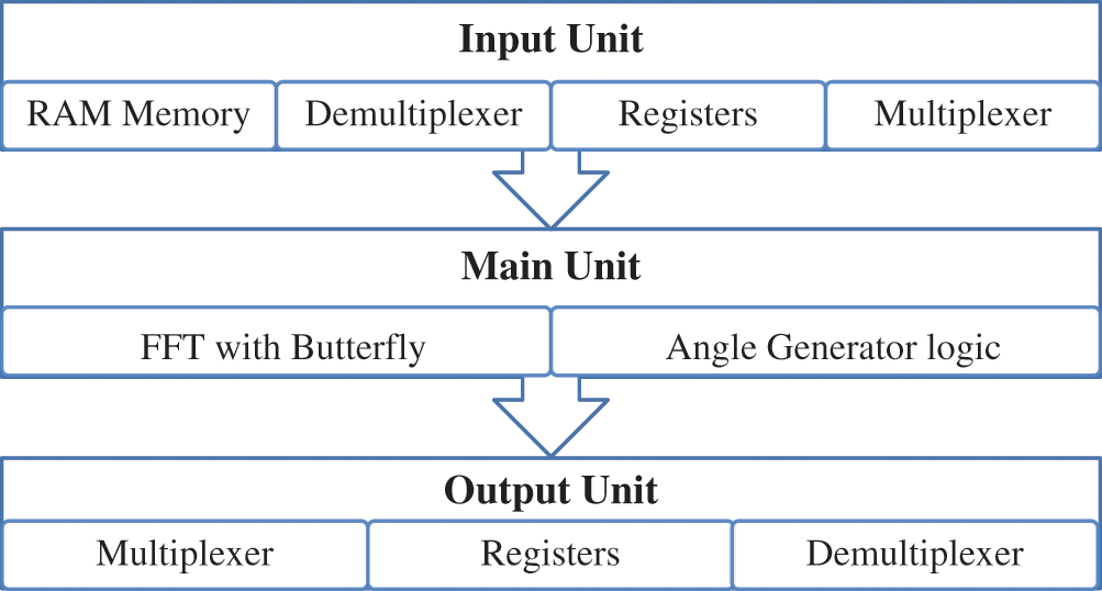
Figure 2: CORDIC based FFT functional blocks
An angle generator unit generates the intermediate phases of the twiddle factor angles generated by the rotation and pipelined architecture of the CORDIC algorithm. The demultiplexer takes the data from butterfly output, stores it in corresponding registers, and sends using multiplexers. In the FFT computation, researchers have used the multibank addressing scheme to realize the pipelined and parallel architecture of FFT, but these techniques will not be suitable for less memory hardware following the CORDIC algorithm. In their solution, the twiddle factor angle is not increasing and enriches the complexity in design for angle generator unit.
Fig. 3 shows the block diagram of the angle generator unit, which follows the regular incremental steps generated by a simple accumulator. The accumulator is comprised of an adder and a register. The phase angle (2π/N) values are given to the adder and stored in the register enabled by the clock signal. The registered output is feedback to the adder for increment in input angle value. Further, the angle is given to the latch to provide the actual generated angle as output based on the control input.
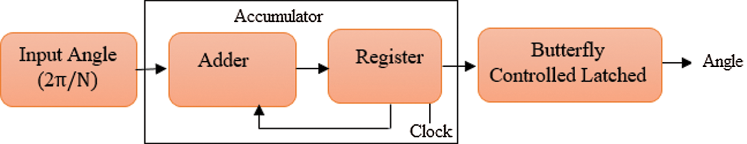
Figure 3: Angle generation scheme
Tab. 1 lists the angle generator for radix-2 FFT twiddle factor (N = 2, 4, 8, 16, 32….1024). Tab. 2 lists RAM address generation and corresponding twiddle factor angles for 32-point radix-2 FFT. The twiddle factor angle is increasing sequentially concerning the 4-bit butterfly counter (n3, n2, n1, n0) for 32-point FFT. Each angle is the multiplication of the (2π/N), which is π, π/2, π/4, π/8 and π/16 for FFT (N = 2, 4, 8, 16, and 32) respectively. It is easily understood that the twiddle factors for 16-point FFT and 32-point FFT are increasing with a one-step increment of the clock signal.


Figure 4: CORDIC based radix-2 FFT [25]


Figure 5: CORDIC based radix-4 FFT [25]
Figs. 4 and 5 present the radix-2 FFT and radix-4 FFT architecture based on the CORDIC algorithm respectively. The architecture does not have a twiddle factor memory, and CORDIC based angle generator [35] module is associated with the butterfly structure of the design. The design of radix-2 is based on 4 registers, 4 multiplexers, and 4 de-multiplexer. In the same way, radix-4 will require 8 registers and 8 multiplexers, and 8 de-multiplexer. The registers are used to store the contents present prior and post the butterfly module for buffering the intermediate data for the collection of two consecutive butterfly operations together and sine and cosine operations are performed [36]. The register buffer operation can be extended to any value of radix FFT design. The radix-r, FFT design will require 2 x r registers.
The design of the OFDM transceiver chip is followed based on the bottom-up approach in which all the submodules of the transmitter and receiver are designed independently. The OFDM transceiver is designed in Xilinx Vivado 17.4 and synthesized on the Virtex-5 FPGA kit. The process of FPGA synthesis is depicted in Fig. 6.

Figure 6: FPGA synthesis
The design is simulated for a variable length of 8 point-1024-point FFT and IFFT. The simulation waveform for the successful data stream transfer is shown in Fig. 7a and experimental verification on Virtex-5 FPGA is shown in Fig. 7b. The register transfer level (RTL) of the OFDM system has a clock, reset, OFDM_data_in [15:0], as the inputs of the transmitter section, and OFDM_data_out [15:0] as the output of the receiver section. The 16-bit transmitted data is shown in the LEDs of Virtex-5 FPGA against a synthesized bit file of the OFDM receiver section. This data is analyzed serially one byte at a time. The real-time signal processing inside the FPGA is visualized using Chipscope Pro-Analyzer, which is the inbuilt tool in Xilinx to see the internal signal in FPGA. Fig. 8 depicts the internal signal processing of FFT and OFDM transmitter and receiver in FPGA. The simulation is carried for three test cases with 16-bit data transfer from OFDM transmitter to receiver with 50% duty cycle clock signal. The OFDM_data_in is given using switches on FPGA and OFDM_data_out is observed on corresponding LEDs.
Case 1: OFDM_data_in [15:0] = “1010101010101010” and OFDM_data_out [15:0] = “1010101010101010”.
Case 2: OFDM_data_in [15:0] = “1111000011110000” and OFDM_data_out [15:0] = “1111000011110000”.
Case 3: OFDM_data_in [15:0] = “0011001100110011” and OFDM_data_out [15:0] = “0011001100110011”.

Figure 7: (b) Data transfer in CORDIC based OFDM transceiver
The hardware design report is extracted from the Xilinx software which consists of the information about the hardware used for the FPGA device and its design parameters such as the number of flip flops, the number of logic gates, memory utilization, number of slices, and LUTs. The designer has the right to decide the level of optimization required for the design. The hardware synthesis is done on Digilent manufactured Virtex-5 FPGA kit. The target FPGA device is xc5vlx20t-2-ff323, programmed in Virtex-5 FPGA kit. The timing parameter details are presented in terms of total path delay in nanoseconds (ns), input arrival time before clock pulse, frequency support (maximum), output time after clock pulse, and power consumption in mill watts (mW). Tabs. 3 and 4 present the hardware device utilization and the timing summary of OFDM transceiver with radix-2 and 4 FFT, and OFDM transceiver with CORDIC radix-2 and CORDIC radix-4 FFT algorithm.

Figure 8: Chipscope results (a) FFT (b) OFDM signal in FPGA

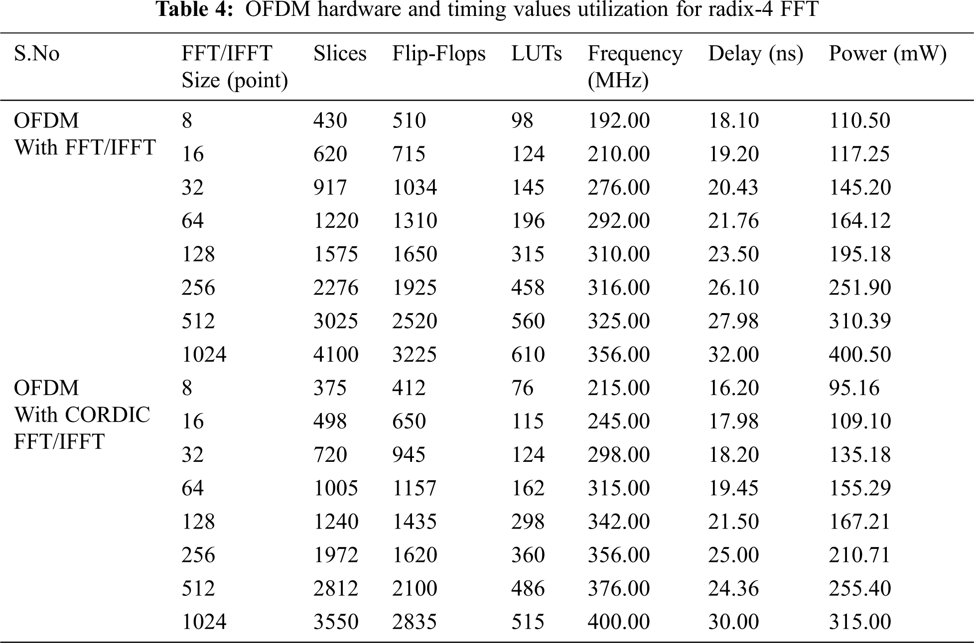

Figure 9: FPGA hardware resources utilization for 1024-point FFT, OFDM system
Fig. 9 shows the comparative graph of hardware utilization parameters of 1024-point radix-2 and 1024-point radix-4 FFTs for the OFDM system on FPGA. The graph depicts that slices, flip-flops, LUTs utilization for radix-2, CORDIC-FFT based OFDM are less in comparison to normal radix-2, FFT based OFDM. The frequency support of 1024 point, radix-2 and radix 4, CORDIC-FFT based OFDM system is greater than 1024-point radix 2 and radix 4, normal FFT based OFDM system that signifies the higher speed of the developed chip. In the same way, the combinational path delay and power consumption are less in the CORDIC-based OFDM system.
Sood et al. [28] implemented the OFDM transceiver chip using radix-2 variable FFT targeted Virtex-5 FPGA. The hardware resource utilization on FPGA was: slices (1775), flip-flops (2217), and LUTs (2217). In our design of the OFDM transceiver chip, the hardware resource utilization on FPGA is slices (1500), flip-flops (1625), and LUTs (220). The OFDM transceiver chip with CORDIC, the hardware resources utilization on FPGA is slices (1275), flip-flops (1575), and LUTs (205). The OFDM system chip design using CORDIC-based FFT is optimal in terms of FPGA hardware utilization.
Funding Statement: The authors received no specific funding for this study.
Conflicts of Interest: The authors declare that they have no conflicts of interest to report regarding the present study.
1. A. Ganguly and A. Banerjee, “VLSI architecture for analog radix-4 DFT front-end in QAM-OFDM receiver,” Analog Integrated Circuits and Signal Processing, vol. 102, no. 1, pp. 169–179, 2020. [Google Scholar]
2. R. Van Nee and R. Prasad, “Basics of OFDM and Synchronization,” in OFDM for Wireless Multimedia Communications, 1st ed., vol. 1. Norwood, MA, USA: Artech House, pp. 117–146, 2000. [Google Scholar]
3. K. Singh, K. S. Bhatia, H. S. Ryait and H. Kaur Bains, “Combating eliminating dispersion-induced fading using suppressed carrier link for OFDM signal,” International Journal of Electronics, vol. 104, no. 4, pp. 583–592, 2017. [Google Scholar]
4. B. S. Krongold and D. L. Jones, “PAR reduction in OFDM via active constellation extension,” IEEE Transactions on Broadcasting, vol. 49, no. 3, pp. 258–268, 2003. [Google Scholar]
5. B. Das, M. F. L. Abdullah, A. A. M. Ahmed and M. M. Shaikh, “Design of cyclic prefix characteristic based OFDM system for wimax Technology,” Wireless Personal Communications, vol. 106, no. 4, pp. 1931–1950, 2019. [Google Scholar]
6. G. G. Kumar, S. K. Sahoo and P. K. Meher, “50 years of FFT algorithms and applications,” Circuits Systems, and Signal Processing, vol. 38, no. 12, pp. 5665–5698, 2019. [Google Scholar]
7. E. Basar, M. Wen, R. Mesleh, M. D. Renzo, Y. Xiao et al., “Index modulation techniques for next-generation wireless networks IEEE,” Access, vol. 5, pp. 1–5, 2017. [Google Scholar]
8. X. Li, Y. Zhang, L. Xiao, X. Xu and J. Wang, “A novel precoding scheme for downlink multi-user spatial modulation system,” in Proc. PIMRC, London, UK, pp. 1361–1365, 2013. [Google Scholar]
9. P. K. Yadav, V. K. Dwivedi, V. Karwal and J. P. Gupta, “A new windowing function to reduce ICI in OFDM systems,” International Journal of Electronics Letters, vol. 2, no. 1, pp. 2–7, 2014. [Google Scholar]
10. S. Y. Park, N. I. Cho, S. U. Lee, K. Kim and J. Oh, “Design of 2K/4K/8K-point FFT processor based on CORDIC algorithm in OFDM receiver,” in Proc. PACRIM, Victoria, Canada, pp. 457–460, 2001. [Google Scholar]
11. C. S. Peng, Y. S. Chuang and K. A. Wen, “CORDIC-based architecture with channel state information for OFDM baseband receiver,” IEEE Transactions on Consumer Electronics, vol. 51, no. 2, pp. 403–412, 2005. [Google Scholar]
12. J. Granado, A. Torralba, J. Chavez and V. Baena-Lecuyer, “Design of an efficient CORDIC-based architecture for synchronization in OFDM,” IEEE Transactions on Consumer Electronics, vol. 52, no. 3, pp. 774–782, 2006. [Google Scholar]
13. K. I. Lee, J. H. Kim, J. K. Lee and Y. S. Cho, “A compact CORDIC algorithm for synchronization of carrier frequency offset in OFDM modems,” IEICE Transactions on Communication, vol. 89, no. 3, pp. 952–954, 2006. [Google Scholar]
14. Cheng-Ying Yu, “Sau-Gee Chen and Jen-Chuan Chih, Efficient CORDIC Designs for Multi-Mode OFDM FFT,” in Proc. ICASSP, Barcelona, Spain, pp. 1036–1039, 2006. [Google Scholar]
15. C. L. Wey, S. Y. Lin and W. C. Tang, “Efficient memory-based FFT processors for OFDM applications,” in Proc. IEIT, pp. 345–350, 2007. [Google Scholar]
16. J. Lee, H. Lee, S. I. Cho and S. S. Choi, “A high-speed low-complexity two-parallel radix- 24 FFT/IFFT processor for UWB applications,” in Proc. ASSCC, pp. 284–287, 2007. [Google Scholar]
17. F. Angarita, M. J. Canet, T. Sansaloni, A. Perez-Pascual and J. Valls, “Efficient mapping of CORDIC algorithm for OFDM-based WLAN,” Journal of Signal Processing System, vol. 52, pp. 181–191, 2008. [Google Scholar]
18. O. A. Alim, N. Elboghdadly, M. A. Ashour and A. M. Elaskary, “FPGA implementation for an optimized CORDIC module for OFDM system,” in Proc. ICCES, Cairo, Egypt, pp. 21–26, 2008. [Google Scholar]
19. J. Han and Y. Jang, “A residual frequency offset synchronization scheme using a simplified CORDIC algorithm in OFDM systems,” in Proc. AUSCTW, Sydney, NSW, Australia, pp. 67–70, 2009. [Google Scholar]
20. B. Lakshmi and A. S. Dhar, “CORDIC architectures: A survey,” VLSI Design, vol. 2010, no. 794891, pp. 1–19, 2010. [Google Scholar]
21. B. Lakshmi and A. S. Dhar, “VLSI architecture for low latency radix-4 CORDIC,” Journal of Computers and Electrical Engineering, vol. 37, no. 6, pp. 1032–1042, 2011. [Google Scholar]
22. T. Y. Sung, H. C. Hsin and Y. P. Cheng, “Low-power and high-speed CORDIC-based split-radix FFT processor for OFDM systems,” Digital Signal Processing, vol. 20, no. 2, pp. 511–527, 2010. [Google Scholar]
23. S. R. Penubolu and R. R. Gudheti, “Performance comparison of autocorrelation and CORDIC algorithm implemented on FPGA for OFDM based WLAN,” in Proc. ICCSN, Xian, China, pp. 575–582, 2009. [Google Scholar]
24. S. Bidwai, S. S. Bidwai, D. S. P. Patil and S. S. Shinde, “Implementation and performance analysis of CORDIC in OFDM based WLAN system using VHDL,” International Journal of Electronics and Communication Engineering & Technology, vol. 3, no. 3, pp. 103–111, 2012. [Google Scholar]
25. E. Oruklu, X. Xiao and J. Saniie, “Reduced memory and low power architectures for CORDIC-based FFT processors,” Journal of Signal Processing Systems, vol. 66, pp. 129–134, 2012. [Google Scholar]
26. N. R. Raajan, B. Monisha, K. Vinoth, R. Niranjan and D. D. Padmanabhan, “CORDIC based modified OFDM for pipelined data process,” Procedia Engineering, vol. 38, pp. 3300–3307, 2012. [Google Scholar]
27. M. Beheshti, M. J. Omidi and A. M. D. Hoseini, “Joint compensation of transmitter and receiver IQ imbalance for MIMO-OFDM over doubly selective channels,” Wireless Personal Communications, vol. 70, no. 2, pp. 537–559, 2013. [Google Scholar]
28. S. Sood, A. P. Singh and A. Kumar, “VHDL design of OFDM transceiver chip using variable FFT,” Journal of Selected Areas in Microelectronics, vol. 5, pp. 47–58, 2013. [Google Scholar]
29. N. Kirubanandasarathy and K. Karthikeyan, “Design of pipeline R2MDC FFT for implementation of MIMO OFDM transceivers using FPGA,” Telecommunication Systems, vol. 63, no. 3, pp. 465–471, 2016. [Google Scholar]
30. A. Kumar, A. Kumar, A. Devrari and S. Singh, “Design and FPGA Implementation of 32-Point FFT Processor,” in Proc. ICICCD, Dehradun, India, pp. 285–292, 2017. [Google Scholar]
31. J. S. Bruno, V. Almenar and J. Valls, “FPGA Implementation of a 10 GS/s variable-length FFT for OFDM-based optical communication systems,” Microprocessors and Microsystems, vol. 64, pp. 195–204, 2019. [Google Scholar]
32. M. Heidarpur, A. Ahmadi, M. Ahmadi and M. R. Azghadi, “CORDIC-SNN: On-FPGA STDP Learning with Izhikevich Neurons,” IEEE Transactions on Circuits and Systems I: Regular Papers, vol. 66, no. 7, pp. 2651–2266, 2019. [Google Scholar]
33. P. K. Meher and S. Y. Park, “Design of cascaded CORDIC based on precise analysis of critical path,” Electronics, vol. 8, no. 4, pp. 1–15, 2019. [Google Scholar]
34. J. E. Volder, “The birth of CORDIC,” Journal of VLSI Signal Processing, vol. 25, no. 2, pp. 101–105, 2000. [Google Scholar]
35. J. Valls, T. Sansaloni, A. Perez-Pascual, V. Torres and V. Almenar, “The use of CORDIC in software defined radios: A tutorial,” IEEE Communication Magazine, vol. 44, no. 9, pp. 46–50, 2006. [Google Scholar]
36. E. I. Garcia, R. Cumplido and M. Arias, “Pipelined CORDIC design on FPGA for a digital sine and cosine waves generator,” in Proc. ICEEE, Bali, Indonesia, pp. 1–4, 2006. [Google Scholar]
 | This work is licensed under a Creative Commons Attribution 4.0 International License, which permits unrestricted use, distribution, and reproduction in any medium, provided the original work is properly cited. |