DOI:10.32604/csse.2022.021205
| Computer Systems Science & Engineering DOI:10.32604/csse.2022.021205 | |
| Article |
Design of Miniature UWB-Based Antenna by Employing a Tri-Sectional SIR Feeder
1Electrical and Computer Engineering Department, Altinbas University, Istanbul, Turkey
2Medical Instrumentation Engineering Department, Al-Esraa University College, Baghdad, Iraq
*Corresponding Author: Ehab Dh. Hussein. Email: ehab.hussein@ogr.altinbas.edu.tr
Received: 26 June 2021; Accepted: 23 August 2021
Abstract: A novel ultra-wideband (UWB)-based microstrip antenna is presented in this work by using a slotted patch resonator, a tri-sectional stepped impedance resonator (SIR) feeder, as well as a reduced ground plane. The whole structure was realized on an FR4 substrate. The impact of incorporating several cases of ground planes on the input reflection has been thoroughly investigated under the same tri-sectional SIR feeder and by employing a slotted patch radiator. Since the complete ground plane presents an inadequate frequency response, by reducing the ground plane, the induced UWB responses are apparent while the antenna exhibits higher impedance bandwidth. The impact of both the uniform impedance resonator (UIR) as well as the SIR feeder on the input reflection has also been examined by following the same adopted reduced ground technique and using a slotted patch radiator. As a result, the UIR feeder exhibits a dual-band frequency response, when a wide notched band is incorporated in the range from 4.5–6.5 GHz. The dual-band response of the bi-sectional SIR feeder is still apparent with a narrower notched band in the frequency range from 4–5 GHz. As far as the tri-sectional SIR feeder is concerned, the UWB response is discernible without recording the existence of a notched band. Additionally, the antenna displays a higher impedance bandwidth compared with the previously reported steps. Our proposed antenna configuration is designed with highly compact dimensions and an overall size of 14 × 27.2 mm2. Moreover, it operates under the impedance bandwidth of 2.86–10.31 GHz that can be leveraged for numerous applications where wireless systems are used. Our approach presents several advantages compared with the other reported UWB-based antennas in the literature, whereas the measured S11 pattern is in good agreement with the simulated one.
Keywords: Microstrip antenna; reduced ground plane; slotted patch radiator; tri-sectional stepped impedance feeder; ultra-wideband
Antennas are considered as a system capable of consecutively transmitting and receiving signals. Therefore, the relative speed of the dispatching and receiving process is of great importance for the rapid growth of the various communications technologies. However, the tremendous expansion of the fixed and mobile communication networks requires an increase of the high data rate for a broader frequency range due to the significant rise of the network users. Consequently, there is an urgent need for both the mobile and the wireless networks to exploit a wider bandwidth (BW). Therefore, it is of great importance to developing ultra-wideband (UWB) and low-profile antennas by keeping at the same time the design complexity and manufacturing cost at minimum levels [1].
Along these lines, the UWB technology stands for an up-and-coming solution for the implementation of wireless communication systems since it exhibits several advantages, including low power consumption, high data rating, exceptional tolerance to multipath propagation, and a high level of reliability. Additionally, the UWB-based approach has the ability to operate in a wideband frequency spectrum by covering the high-frequency range, which is employed for the further localization of the microwave energy at a particular target. In contrast, the low-frequency region is used since it allows the deep penetration of the microwave signal over several barriers [2].
Moreover, the desired characteristics of the antennas under consideration should be taken into account before designing wide-speed and UWB-based antennas. Furthermore, in order to fabricate microstrip antennas with enhanced energy efficiency, a detailed study of the various employed structures, analyses, and feeding methods is required. The patch antenna is regarded as the best option for the design of microwave configurations due to the employment of cost-effective and lightweight materials, as well as the use of precise manufacturing techniques. There are several reports in the literature that have dealt with the improvement of the antenna parameters in order to increase both the design performance and quality of the patch antenna. Among the various parameters that could be tuned are the return loss, gain, path, and total bandwidth [3,4]. Furthermore, the associated BW work based on the Federal Communications Committee (FCC) and the appropriate frequency bandwidth region should be taken into account for the design and application of the UWB antenna. According to the US-Canada UWB standard, for example, there are no limits on the BW [5] for the following frequency range: 3.1–10.6 GHz. Many types of the UWB-based antennas were presented in Ref. [6], accompanied by an examination of their architecture, design techniques, and output efficiency. In addition, two-dimensional and three-dimensional structures of antennas have been employed for communications applications. The selection of a specific type of antenna mainly depends on the underlying specifications of the desired application [7]. For instance, some of them can be employed for the robust operation of a big network of mobile devices. The low-profile transceivers do not occupy a big area of the printed circuit board while they can also be used for the development of body networks for mobile devices or wireless sensors. In addition, antennas also exhibit flexibility properties within wireless body networks since they can be bent at nearly 90 degrees [8,9].
In total, a communications transceiver system is composed of the following components: a widescreen microstrip, a broadband monopole antenna, UWB wide-slot antenna, UWB antenna, taper slot UWB antenna, UWB aerial, a metamaterial, and the dielectric resonator aerials antenna. The transceivers are used in order to receive the communication packages. These types of antennas were updated since their efficiency had to be improved in view of fabricating robust transceivers. Dielectric Resonator (DR) is also actively employed in the antenna design, which is called Dielectric Resonator Antenna (DRA). DRs are actually dielectric materials that, under the enforcement of a particular frequency, exhibit resonance peaks. These structures have already demonstrated a high Q-factor and operation within a specific frequency range. The final structure should include a DR, a ground plane, and an excitement source in order to provide DR-based antenna radiation [10].
In Ref. [11], a new type of UWB-based microstrip antenna has been proposed. More specifically, a rectangular radiator patch has been employed with dual L-shaped slots in order to expand the current path to both sides of the radiating patch. Moreover, a two-step impedance resonators structure was incorporated at the one end of the radiation patch and the antenna feeder in order to realize a broadband impedance bandwidth from 2.39 to 13.78 GHz.
The goal of the current work is the design a new microstrip patch antenna with some new features, such as high compactness and ultra-wideband operation. In order to attain these characteristics, a single-layer substrate was firstly employed in order to include the tri-sectional step impedance resonator feeder and the slotted patch resonator. In addition, a reduced ground plane was used in the design. Insights from our parametric studies based on the ground plane and SIR feeder design steps have divulged that the projected antenna’s impedance bandwidth and the input reflection have been optimized by the employment of a tri-sectional SIR feeder and a specific reduced ground unit.
2 Step Impedance Resonator (SIR)
The SIR resonator has the ability to adjust the harmonic frequency distribution based on the frequency response. This is achieved by regulating the impedance ratio and the resonator length in order to compensate for the unequal phase velocity of the odd and even modes. A broader frequency band can be realized by suitably selecting the physical structural parameters due to the use of cost-effective materials and simple topology architectures. The SIR structure could be designed in order to have more diminutive dimensions than the uniform impedance resonator (UIR), which is widely used in RF and microwave devices [11,12]. The respective configurations of both the UIR and the SIR structures are schematically illustrated in Fig. 1. As far as the SIR topology is concerned, two microstrip transmission lines are employed. The lines have dissimilar characteristic impedances (
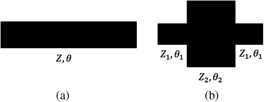
Figure 1: Depiction of the (a) UIR and (b) The respective SIR configurations
The SIR scheme originates from a conventional microstrip resonator, which introduces step-impedance perturbations. Fig. 2 depicts the related SIR configurations.
The performance of the SIR topology can be investigated by considering an even/odd-mode analysis due to symmetry issues. Along these lines, Fig. 3 illustrates the even and odd equivalent circuits, whereas the employed equations for the even and odd input impedances are the following [13]:
where
Based on the resonant condition,
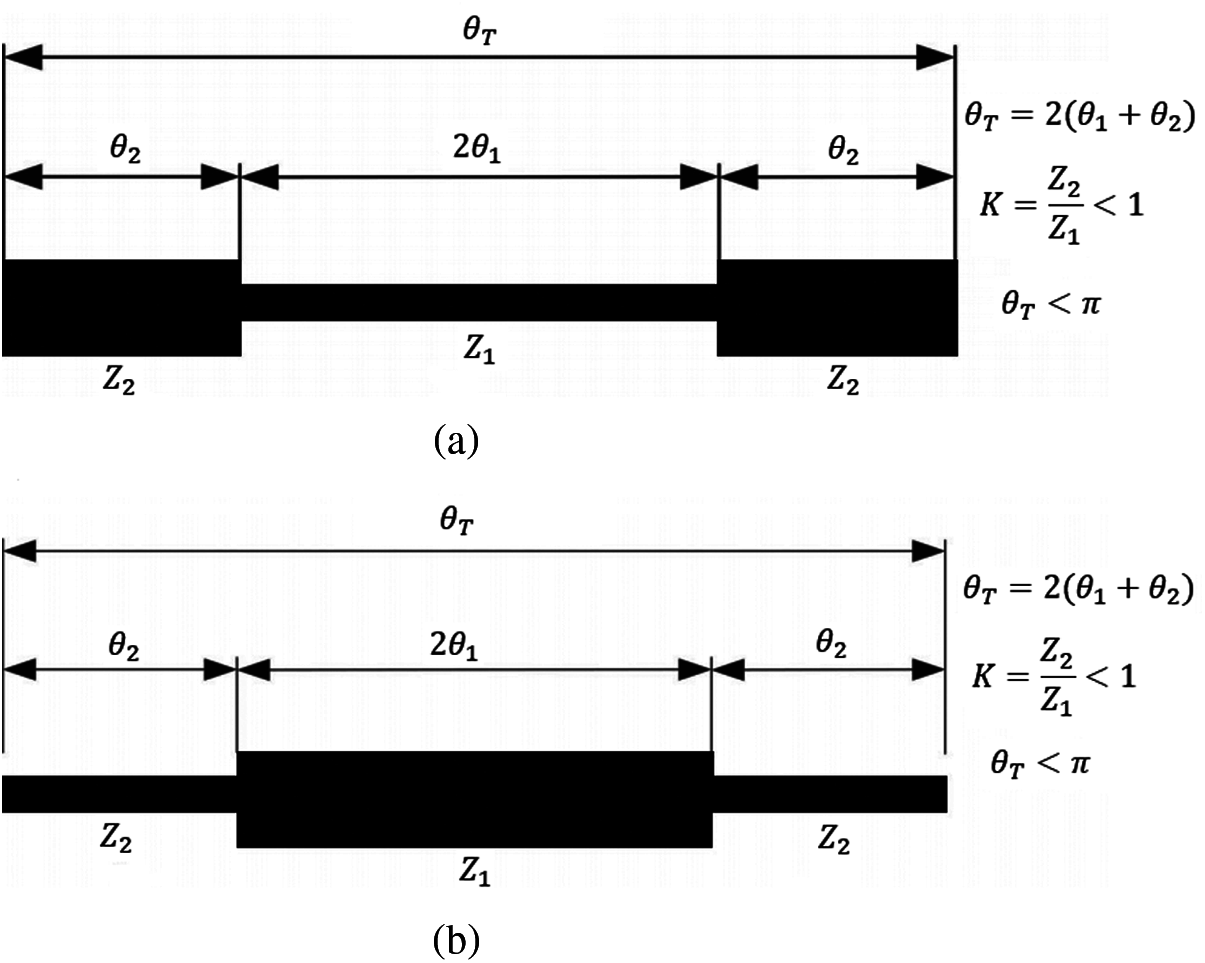
Figure 2: Detailed depiction of the SIR configurations
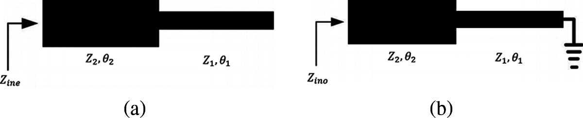
Figure 3: Equivalent circuit of the (a) Even and (b) Odd modes of the SIRs configurations, respectively
From the above-mentioned equation, the ratio
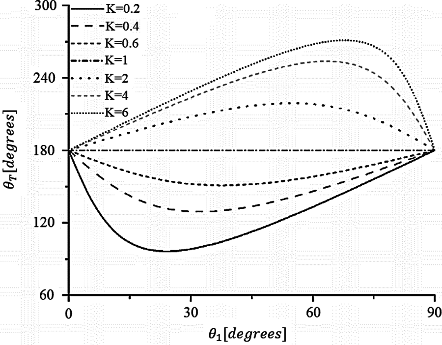
Figure 4: Distribution of
By selecting the value of
Fig. 4 reveals the dependence of
In order to investigate the ratio of the fundamental and the higher-order resonances modes, the case where
and the resonant conditions are the following:
Based on Eq. (5), the ratios of the resonant frequencies can be derived based on:
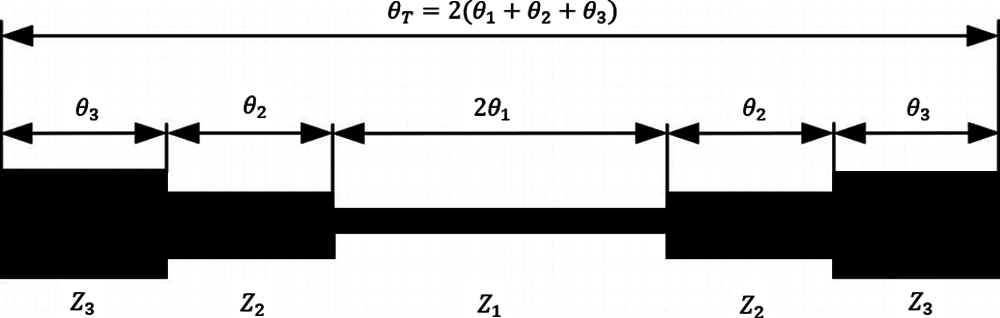
Figure 5: Configuration of the tri-stage stepped-impedance resonator
More specifically, the f1 mode does not stand for the conventional harmonic behavior but consists of two resonant modes in conjunction with the basic mode. In addition,
Correspondingly, we can extract the following value:
The tri-mode SIR-based effect can be implemented since the structure has the ability to support three resonant modes. Fig. 5 discloses the respective SIR configuration that is composed of three segments with dissimilar impedance values. The even-/ odd-mode analysis can be adopted in order to evaluate the total structure behavior. The corresponding circuits are illustrated in Fig. 6, and the employed equations are described as follows:
where
The essential and dual higher resonances arise when the following conditions are satisfied:

Figure 6: Equivalent circuits for the (a) Even and (b) Odd modes
The mode ratios can be determined by:
where
We have to underline that only
Slot antennas have gained increased popularity due to their ultra-wideband characteristics. As a result, these are widely used for broadband and volume-limited applications [1,14].
The proposed structure of the UWB-based antenna is schematically illustrated in Fig. 7. This antenna is etched on an FR-4 substrate with a relative permittivity value of 4.3 and a thickness of 1.5 mm. The feeder is actually a tri-stage stepped structure with impedance values of 50, 100 and 200 Ω, electrical lengths of 5, 5 and 5 mm, and widths of 3, 1.8 and 1.1 mm.
The ground regions that appear in the bottom layer are designed with a length and width of 11.95 and 11 mm, respectively, while a 0.035 mm ground thickness was selected for all modules. For the substrate, the following dimensions were employed: 14 mm width, 27.2 mm length, and 1.5 mm thickness.

Figure 7: Top and back views of the projected UWB antenna
The simulated input reflection response of the antenna by using the CST MWS simulator is revealed in Fig. 8. At the resonant frequency values of 3.25 and 6.27 GHz, an input reflection of −22.5 and −28.5 dB is obtained, respectively. Furthermore, the total bandwidth of the antenna is 7.45 GHz.

Figure 8: Input reflection of the proposed UWB antenna
The Voltage Standing Wave Ratio (VSWR) is 1.1621 at 3.25 GHz and 1.0781 at 6.27 GHz, as depicted in Fig. 9. The VSWR value can be calculated by using the following equation:

Figure 9: Distribution of the VSWR response of the proposed UWB antenna
The gain of the microstrip antennas presents a strong dependence on the substrate material properties. More specifically, the gain is inversely proportional to the static dielectric constant ϵr and straightforwardly proportional to substrate thickness. For the projected antenna, the highest directivity gain is 2.16 dB at 5.2 GHz, as it is illustrated in the 3D radiation patterns in Fig. 10.
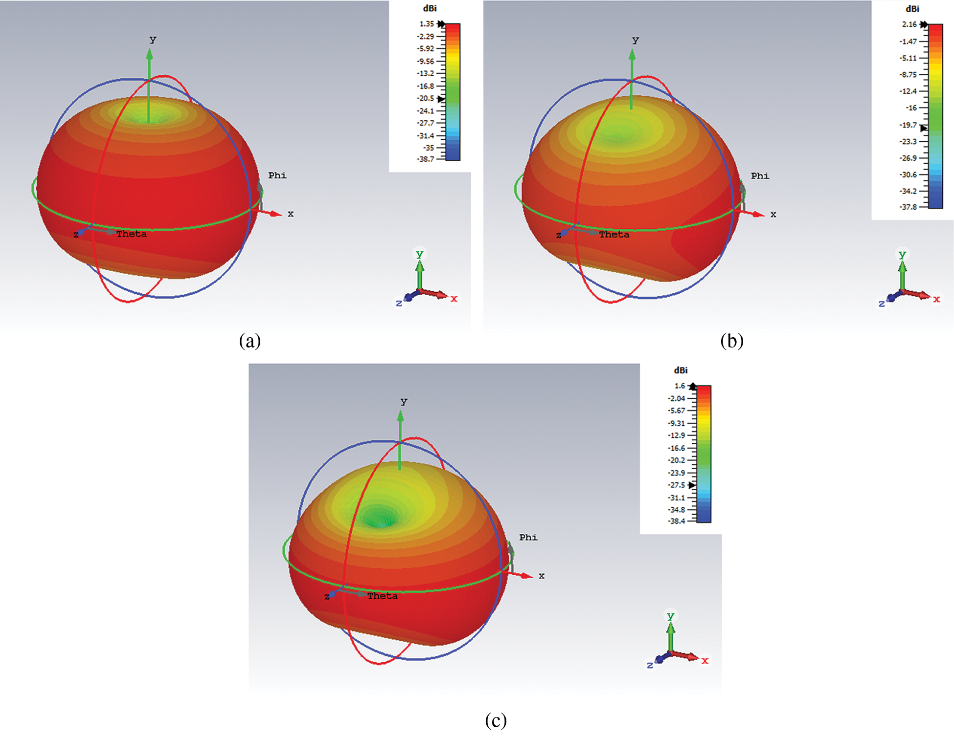
Figure 10: 3D simulated radiation patterns of the projected UWB antenna at (a) 3.2 GHz, (b) 5.2 GHz and (c) 6.4 GHz
Fig. 11 divulges the simulated surface current distribution in the conductive regions of the projected UWB-based antenna. The effective areas with high current intensity are discernible in this image, including the SIR feeder, the bottom layer of the patch radiator, and some edges of the reduced ground plane with the maximum current intensity of 5 A/m.

Figure 11: Distribution of the surface current intensity of the antenna
The IEEE gain of the UWB antenna within the impedance bandwidth of 2.86–10.31 GHz is disclosed in Fig. 12. Fig. 13 reveals the simulated far–distance patterns’ radiation fields in the x–y, x–z and y–z planes. The radiation patterns along the xy plane represent the horizontal component since they are perpendicular to the E plane and coincided with the H-plane of the vertically polarized antenna. On the other hand, the E plane coincides with the yz plane. Therefore, the yz patterns can be considered as the vertical plane radiation patterns.
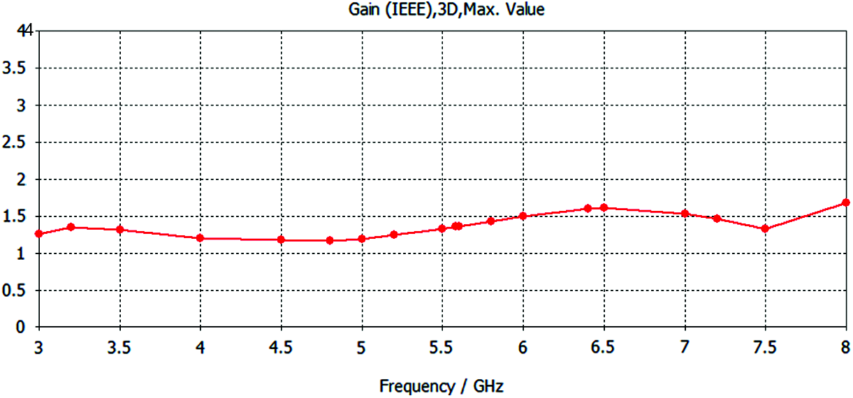
Figure 12: Gain of the designed UWB antenna

Figure 13: Radiation patterns of the designed UWB antenna under the application of the frequency value of (a) 3.25 GHz and (b) 6.27 GHz
The proposed UWB antennas in this study have been compared with similar works that have been reported in the literature [15–28]. From the provided results that are illustrated in Tab. 1, the projected antenna of this work exhibits the smallest size and a relatively big impedance bandwidth.

5.1 Effect of the Ground Plane on the Input Reflection Response
In this sub-section, the impact of various types of ground planes on the input reflection performance, as it is depicted in Fig. 14, has been investigated by considering the same tri-sectional SIR feeder and the employed slotted patch radiator. Accordingly, Fig. 15 divulges that the complete ground plane has an inadequate frequency response during the implementation of Step 1. As far as Step 2 is concerned, the dual-band response is obvious, but minor matched operating frequencies are detected. Finally, for Steps 3 and 4, the acquired UWB responses are apparent, while the antenna exhibits a relatively higher impedance bandwidth in Step 4 than Step 3.

Figure 14: Illustration of the various types of the ground plane

Figure 15: Ground plane effect on the input reflection response
5.2 Effect of UIR and SIR Feeder on the Input Reflection Response
In this sub-section, a detailed analysis of the influence of the various types of feeder, which are schematically illustrated in Fig. 16, is carried out. The distribution of the input reflection has been investigated by considering the same adopted dimensions of the reduced ground plane and employed slotted patch radiator, as it is depicted in Fig. 7. In view of that, Fig. 17 discloses that a uniform impedance resonator (UIR), as in Step 1, presents a dual-band frequency response accompanied by a wide notched band from about 4.5 to 6.5 GHz. In Step 2, the dual-band pattern is apparent, but a narrower notched band within the frequency range from 4 to 5 GHz has been recorded. Finally, in Step 3, the UWB response is discernible but without detecting a notched band region, whereas the antenna exhibits a higher impedance bandwidth than the previous steps.

Figure 16: Depiction of the various steps during the design of the SIR feeder, (a) UIR feeder, (b) Bi-sectional SIR feeder, and (c) Tri-sectional SIR feeder

Figure 17: SIR effect on input reflection response
6 Fabrication and Measurements
The proposed UWB antenna was fabricated by using an LPKF ProtoMat S63, including all the design steps and optimization procedures. Firstly, on the FR4 epoxy substrate, a prototype was milled and an SMA coaxial connector was used, as it is disclosed in Fig. 18, for the connection of the feedline end. Then, the Anritsu Vector Network Analyzer was used in order to experimentally test our prototype.
Both the measured and simulated antenna results are presented in Fig. 19. From the extracted results, we can draw the conclusion that a good agreement between the experimental data and the simulated predictions has been attained. However, we can still discern some variations between the two approaches, which can be interpreted by considering the impact of the experimental conditions. More specifically, the SMA connector efficiency, soldering effect, the manufacture tolerance, and the dielectric substrate losses are main reasons for these variations.

Figure 18: Images of the prototype shots of the designed UWB antenna: (a) Top view and (b) Bottom view

Figure 19: Measured and simulated S11 results of the designed UWB antenna
A new type of miniature UWB-based antenna was fabricated and simulated by employing a slotted patch resonator, a tri-sectional SIR feeder, and a reduced ground plane. The antenna was printed on an FR-4 substrate with a dielectric constant of 4.3 and a thickness of 1.5 mm. Moreover, a tri-stage SIR feeder was used with impedances values of 50, 100 and 200 Ω and an electrical length of 5 mm for each section. Except from the highly compact structure of the designed antenna, the acquired scattering response revealed the existence of the dual resonances at 3.25 and 6.27 GHz accompanied with a UWB impedance bandwidth of 7.45 GHz and tolerable input reflection. The proposed antenna configuration possesses the smallest size with enhanced impedance bandwidth compared with numerous reported UWB-based antennas in the literature. Our work can be used for the future development of a robust tumor detector that could assist the early diagnosis of various cancer diseases.
Acknowledgement: The authors thank TopEdit (www.topeditsci.com) for its linguistic assistance during the preparation of this manuscript.
Funding Statement: This research was supported by the Altinbas University, Istanbul, Turkey.
Conflicts of Interest: The authors declare no conflict of interest to report regarding the present study.
1. T. Saeidi, I. Ismail, W. P. Wen, A. R. H. Alhawari and A. Mohammadi, “Ultra-wideband antennas for wireless communication applications,” International Journal of Antennas and Propagation, vol. 2019, no. 4, pp. 1–25, 2019. [Google Scholar]
2. H. Tizyi, F. Riouch, A. Tribak, A. Najid and A. Mediavilla Sanchez, “CPW and microstrip line-fed compact fractal antenna for UWB-RFID applications,” Progress In Electromagnetics Research, vol. 65, pp. 201–209, 2016. [Google Scholar]
3. W. R. Deal, T. Jung, M. C. Wu and T. Itoh, “All-optically controlled beam-scanning array for antenna remoting applications,” in Proc. IEEE MTT-S Int. Microwave Symposium Digest (Cat. No.98CH36192Baltimore, MD, USA, vol. 3, pp. 1383–1386, 2002. [Google Scholar]
4. Y. M. M. Antar, “Microstrip antenna design handbook [Book Review],” IEEE Antennas and Propagation Magazine, vol. 45, no. 2, pp. 86, 2003. [Google Scholar]
5. R. Cicchetti, A. Faraone, D. Caratelli and M. Simeoni, “Wideband, multiband, tunable and smart antenna systems for mobile and UWB wireless applications 2014,” International Journal of Antennas and Propagation, vol. 2015, pp. 1–3, 2015. [Google Scholar]
6. G. M. Galvan-Tejada, M. A. Peyrot-Solis and H. Jardon Aguilar, Ultra Wideband Antennas: Design, Methodologies, and Performance. London, England: CRC Press, 2017. [Google Scholar]
7. Y. Wang, A. M. Abbosh, B. Henin and P. T. Nguyen, “Synthetic bandwidth radar for ultra-wideband microwave imaging systems,” IEEE Transactions on Antennas and Propagation, vol. 62, no. 2, pp. 698–705, 2014. [Google Scholar]
8. M. K. Chirala, C. Huynh, C. Nguyen and X. Guan, “Design of an ultra-small distributed low-noise-amplifier for ultra-wideband applications,” in Proc. APSURSI, Spokane, WA, USA, pp. 3361–3364, 2011. [Google Scholar]
9. W. Su, “Ultra-wideband signals and systems in communication engineering,” IEEE Signal Processing Magazine, vol. 25, no. 5, pp. 122–123, 2008. [Google Scholar]
10. S. K. K. Dash, T. Khan and Y. M. M. Antar, “A state-of-art review on performance improvement of dielectric resonator antennas,” International Journal of RF and Microwave Computer-Aided Engineering, vol. 28, no. 6, pp. e21270, 2018. [Google Scholar]
11. Z. H. Ma and Y. F. Jiang, “L-shaped slot-loaded stepped-impedance microstrip structure UWB antenna,” Micromachines, vol. 11, no. 9, pp. 1–13, 2020. [Google Scholar]
12. Y. S. Mezaal and A. S. Al-Zayed, “Design of microstrip bandpass filters based on stair-step patch resonator,” International Journal of Electronics, vol. 106, no. 3, pp. 477–490, 2019. [Google Scholar]
13. N. Janković, V. Crnojević-Bengin, P. Meyer and J.-S. Hong, “Design methods of multi-band filters,” in Advances in Multi-Band Microstrip Filters. Cambridge: Cambridge University Press, pp. 5–66, 2015. [Google Scholar]
14. L. Yingsong, W. Li and T. Jiang, “Implementation and investigation of a compact circular wide slot UWB antenna with dual notched band characteristics using stepped impedance resonators,” Radioengineering, vol. 21, no. 1, pp. 517–527, 2012. [Google Scholar]
15. J. Liang, C. C. Chiau, X. Chen and C. G. Parini, “Study of a printed circular disc monopole antenna for UWB systems,” IEEE Transactions on Antennas and Propagation, vol. 53, no. 11, pp. 3500–3504, 2005. [Google Scholar]
16. Y. M. Mohamed, H. Abdallah and E. EI-Hennawy, “Circularly polarized wideband-to narrowband switchable antenna,” IEEE Access, vol. 7, pp. 36010–36018, 2019. [Google Scholar]
17. S. Sadat, M. Fardis, F. Geran, G. Dadashzadeh, N. Hojjat et al., “A compact microstrip square-ring slot antenna for UWB applications,” in 2006 IEEE Antennas and Propagation Society Int. Symp., Albuquerque, NM, USA, pp. 4629–4632, 2006. [Google Scholar]
18. M. Gopikrishna, D. D. Krishna, C. K. Aanandan, P. Mohanan and K. Vasudevan, “Compact linear tapered slot antenna for UWB applications,” Electronics Letters, vol. 44, no. 20, pp. 1174, 2008. [Google Scholar]
19. R. Hussain, M. S. Sharawi and A. Shamim, “An integrated four-element slot-based MIMO and a UWB sensing antenna system for CR platforms,” IEEE Transactions on Antennas and Propagation, vol. 66, no. 2, pp. 978–983, 2018. [Google Scholar]
20. Z. N. Low, J. H. Cheong and C. L. Law, “Low-cost PCB antenna for UWB applications,” IEEE Antennas and Wireless Propagation Letters, vol. 4, pp. 237–239, 2005. [Google Scholar]
21. A. Kundu, U. Chakraborty and A. K. Bhattacharjee, “Design of a compact wideband microstrip antenna with very low VSWR for WIMAX applications,” International Journal of Microwave and Wireless Technologies, vol. 9, no. 3, pp. 685–690, 2017. [Google Scholar]
22. N. George and B. Lethakumary, “A compact microstrip antenna for UWB applications,” Microwave and Optical Technology Letters, vol. 57, no. 3, pp. 621–624, 2015. [Google Scholar]
23. W. Mazhar, M. A. Tarar, F. A. Tahir, S. Ullah and F. A. Bhatti, “Compact microstrip patch antenna for ultra-wideband applications,” in PIERS Proc., Stockholm, Sweden, 2013. [Google Scholar]
24. S. M. Jose and B. Lethakumary, “CPW-fed step-shaped microstrip antenna for UWB applications,” Microwave and Optical Technology Letters, vol. 57, no. 3, pp. 589–591, 2015. [Google Scholar]
25. M. C. Lim, S. K. A. Rahim, M. R. Hamid, A. A. Eteng and M. F. Jamlos, “Frequency reconfigurable antenna for WLAN application,” Microwave and Optical Technology Letters, vol. 59, no. 1, pp. 171–176, 2017. [Google Scholar]
26. F. D. Dahalan, S. K. A. Rahim, M. R. Hamid, M. A. Rahman, M. Z. M. Nor et al., “Frequency-reconfigurable archimedean spiral antenna,” IEEE Antennas and Wireless Propagation Letters, vol. 12, pp. 1504–1507, 2013. [Google Scholar]
27. V. Bhanumathi and S. Swathi, “Bandwidth enhanced microstrip patch antenna for UWB applications,” ICTACT Journal on Microelectronics, vol. 4, no. 4, pp. 669–675, 2019. [Google Scholar]
28. J. Vijayalakshmi and G. Murugesan, “A miniaturized high-gain (MHG) ultra-wideband unidirectional monopole antenna for UWB applications,” Journal of Circuits, Systems and Computers, vol. 28, no. 13, pp. 1950230, 2019. [Google Scholar]
 | This work is licensed under a Creative Commons Attribution 4.0 International License, which permits unrestricted use, distribution, and reproduction in any medium, provided the original work is properly cited. |