DOI:10.32604/csse.2022.020400
| Computer Systems Science & Engineering DOI:10.32604/csse.2022.020400 | |
| Article |
Performance Enhancement of PV Based Boost Cascaded Fifteen Level Inverter for AC Loads
Department of Electrical and Electronics Engineering, Hindusthan College of Engineering and Technology, Coimbatore, 641032, India
*Corresponding Author: M. P. Viswanathan. Email: viswanathanmp2021@gmail.com
Received: 22 May 2021; Accepted: 29 July 2021
Abstract: In this research work, single-stage fifteen levels cascaded DC-interface converter (CDDCLC) is proposed for sun arranged photovoltaic technology (PV) applications. The proposed geography is joined with help DC chopper and H-associate inverter to upgrade the power converter to accomplish the diminished harmonic profile. In assessment with the customary inverter structures, the proposed system is used with diminished voltage stress, decreased switch count and DC source tally. The proposed research work with cascaded DC link converter design requires three DC sources for combining fifteen-level AC output. This investigation structure switching technique is phase opposition and disposition pulse width modulation technique (POPD) which results in improved quality of obtained output AC power with 6.73% THD and also determinedly recommended for power converters used in UPS and drive applications since it is extremely affordable. A simulation and prototype model of fifteen-level CDDCLC system is deployed and its performance is analyzed for various operating conditions.
Keywords: Cascaded DC link converter (CDDCLC); modified phase opposition and disposition (MPOPD PWM); photovoltaic (PV); DC interface boost converter
The new type of power converter options for high-power functions appear in multilevel inverters (MLIs) in power converters, particularly for sustainable power source combinations and uninterruptible power supplies [1,2]. MLI's traditional multilevel inverter topologies are flying capacitor MLI (FCMLI), diode clamped MLI and cascaded multilevel inverter CMLI [3,4]. Each topology has its advantages and limitations. CMLI synthesizes the AC voltage waveform of the staircase from a few DC sources among the setup with decreased consonant substance [5]. So the configuration of CMLI is more desirable than the other two configurations.
In order to achieve the nominal output voltage in CMLI, [6,7], a step-up dc-dc converter is connected between DC sources and H-bridges. In view of the quantity of regulated force switches and DC sources, the feasibility of the CMLI and lift CMLI (BCMLI) configurations [8] is compromised.
Some modifications can be made in the standard CMLI and BCMLI frameworks [9–12] in this process. CMLI with decreased switch count is proposed in this framework. In addition, it is shown that the ostensible yield voltage is obtained by presenting the raise chopper circuit between the DC sources and the DC-interface inverter.
The Boost Chopper Network raises the DC input voltage to the nominal voltage level. This results in the number of DC sources and power switches being decreased. In this paper, for UPS applications, a single-phase fifteen-level asymmetrical source boost DC-link CMLI (BDCLCMLI) system is developed. For DC-link switches [13–21], a multicarrier sinusoidal pulse-width modulation (MCSPWM) switching strategy has been developed to obtain a better quality of AC power with an improved harmonic profile.
For each H-bridge and m-level inverter, a separate DC bus is needed; 2 (m−1) numbers of switches per step and 2 (m−1) numbers of ant parallel diodes are required. Topology of seven level cascaded multilevel inverter with RL load is shown in Fig. 1.
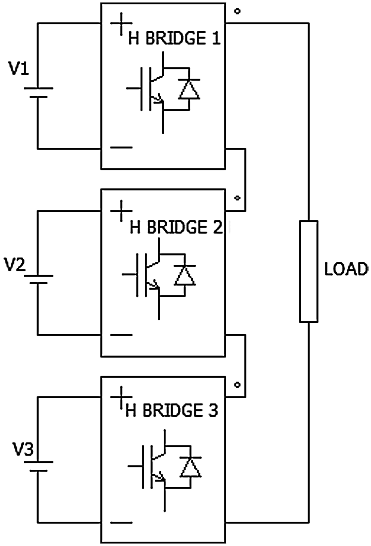
Figure 1: Cascaded multilevel inverter (Seven-level)
A single-phase seven-level asymmetrical source boost converter in deployed in this work. [Uthirasamy et al. (2014)]. The BDCLCMLI (DC-link CMLI) framework is optimized for UPS Applications. The general structure of the BDCLCMLI seven level scheme is shown in Fig. 2. For DC-link switches, multicarrier sinusoidal pulse-width modulation (MCSPWM) switching strategy is built to obtain better quality of AC power (with reduced harmonic content). Circuit diagram of fifteen levels Boost DC-link which is cascaded with multilevel inverter is given in Fig. 3.
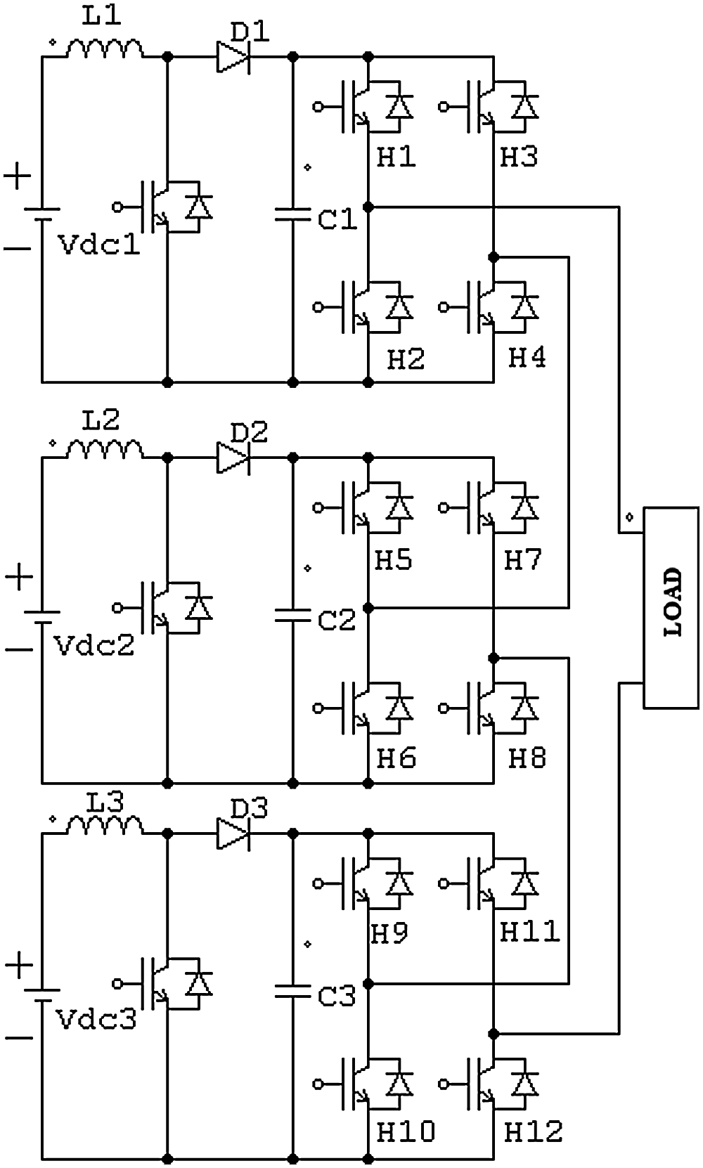
Figure 2: Boost cascaded multilevel inverter (Seven levels)
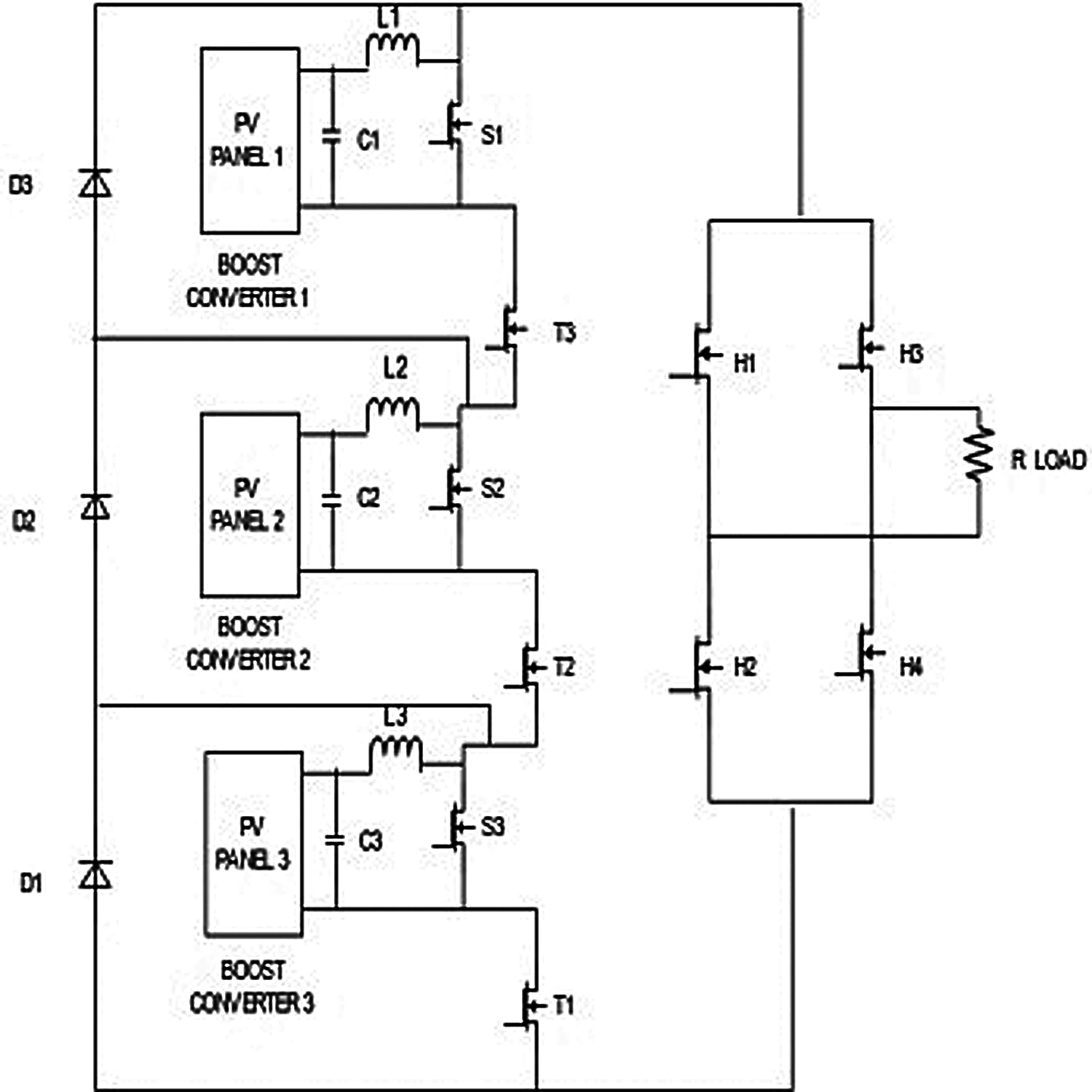
Figure 3: Circuit diagram of fifteen levels boost DC-link cascaded multilevel inverter
The dc/dc converter extricates the greatest power from the dc-interface to the PV series. [Ajami et al. (2013)]. It should be noted that the immediate association of the PV string to the dc-connect, due to the second consonant swaying of the dc-interface, results in a wavering of the PV string's extricated power.
2 Configuration of BDCLCMLI System
Three lopsided DC voltage sources, support chopper unit, DC-connect module (DCLM) and a typical H-connect inverter establish a BDCLCMLI framework. Further, in corresponding to the DC-interface framework H-connect inverter is associated. The BDCLCMLI configuration withholds various numbers of levels and switches which is calculated by Eqs. (1) and (2),
where,
Nlevel- number of levels,
NSwitch-number of switches in BDCLCMLI,
n- Number of boost chopper units.
r- Number of DC source count.
p-Number of H-bridge inverter count.
The proposed topology consists of two parts, they are
i) Boost chopper with Solar input
ii) Level generation unit with Common H bridge
2.1 Boost Chopper with Solar Input
The asymmetrical DC source output voltage is always unidirectional. And each boost chopper unit is connected with asymmetrical DC sources.
Fig. 4 represents the structure of the boost chopper. Believing the framework to be lossless, the normal yield voltage of each lift chopper is gotten using Eq. (3)
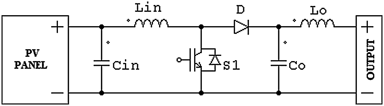
Figure 4: Boost chopper
2.2 Level Generation Unit with Common H Bridge
The proposed asymmetrical multilevel inverter is made up of two parts. They are the Level generation unit and common H Bridge. The boost chopper output voltage of isolated sources is switched via the level generation unit to produce the desired fifteen levels. The switching states are listed in Tab. 1. The asymmetrical topology produces fifteen levels when compared to the symmetrical one whereas the conventional topology produces only seven levels. Hence the topology saves the number of switches and sources.
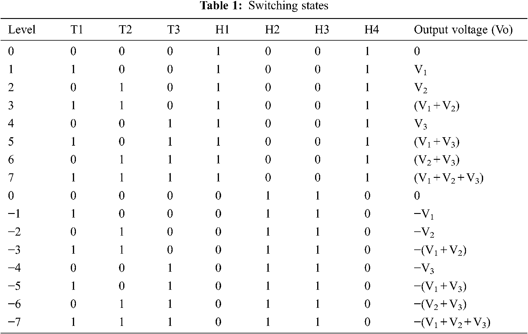
The level generation unit having sub-modules can produce only unidirectional voltage. So a common H bridge is used to reverse the generated voltage. This in turn helps to produce bipolar symmetrical waveform and reduces the individual H bridge at the same time. The switches in the level generation unit are marked as T1, T2 and T3. The common H bridges marked as H1, H2, H3 and H4.
The proposed system is switched under nine states to obtain fifteen-level. The ac output voltage level is controlled through multi carrier PWM. The operation of level generation unit is explained from Mode 1 to Mode 8 as shown in Figs. 5a–5h. The reverse voltage technique is explained through Mode 9 in Fig. 5i.

Figure 5: (a) Mode 1 (V0 = 0 V) (b) Mode 2 (V0 = 1 V) (c) Mode 3 (V0 = 2 V) (d) Mode 4 (V0 = 3 V) (e) Mode 5 (V0 = 4 V) (f) Mode 6 (V0 = 5 V) (g) Mode 7 (V0 = 6 V) (h) Mode 8 (V0 = 7 V) (i) Mode 9 (V0 = −V)
The lift chopper switch Sb is turned ON at t = TON2 and current which flows through inductor L2 varies linearly from I3 to I4
Hence, the voltage across inductor L2 is derived as
Now, vitality contribution to inductor L2 from the source
At t = TOFF2the lift chopper switch Sb is switched OFF and current through the inductor L2 flows linearly from I4 to I3.
Average output voltage of boost chopper II is obtained
During this time, the energy which is released by the inductor L2 to BDCIM is given by,
The change in voltage over the capacitor C2 is derived by
Voltage across the inductor 4 is derived as
The vitality contribution to inductor 4 from source Vd1 is identified as
At t = TOFF1 lift chopper switch Sa is switched OFF and the current which flows through inductor 4 falls linearly from I2 to I1.
At t = TOFF1 lift chopper switch Sa is switched OFF and the current through the inductor 4 falls linearly from I2 to I1
The normal yield voltage of lift chopper I can be expressed as
At this moment the energy which is released by inductor L1 to the BDCLM is given by
The ripple in the inductor current can be obtained as
The adjustment in voltage overCapacitor t1 can be written as
At t = TON3 boost chopper switch Sa and Sb are turned ON and current through the inductors L1 and L2 increases gradually from I1 to I2 and I3 to I4 respectively.
At right now, vitality contribution to inductor L1 from source Vd1 and energy fed to the inductor L2 from source Vd2 are
Boost chopper switches Sa and Sb are switched OFF and current through inductor L1 and L2 drops linearly from I2 to I1 and from I4 to I3.
At this moment the energy discharged from inductor
L1 and L2 to BDCLM is given by,
The adjustment in voltageacross capacitor C1 and C2 is expressed as
The positive half cycle magnitude of AC output voltage are written as
The negative half cycle magnitude of AC output voltage are expressed as
To produce positive or negative seven levels, the switches T1-T3 are operated as per the switching pattern listed in the Tab. 1. The DC-DC boost converter outputs are regulated with the ratio 1:2:4. The H bridge switches are operated as shown in the table to produce the seven level output on both positive and negative sides. Mode 1 –Mode 8 H1& H2 switches are turned ON to produce the positive voltage. Similarly to produce negative output voltage H3&H4 switches are turned ON as shown in Fig. 5i.
4 Modified MCSPWM Switching Technique
PWM techniques are classified corresponding to the switching frequency. Sinusoidal PWM, space-vector PWM and concerned harmonic reduction are created such that it reduces the distortion in MLIs. These are considered to be the existing modulation techniques. Vertical transporter dispersion and even bearer dissemination are the two broad categories of MCS PWM control methods [2]. Fig. 6 shows the unipolar MCSPWM switching pattern. It is elevated to trigger the DC-connect switches of CDDCLC.
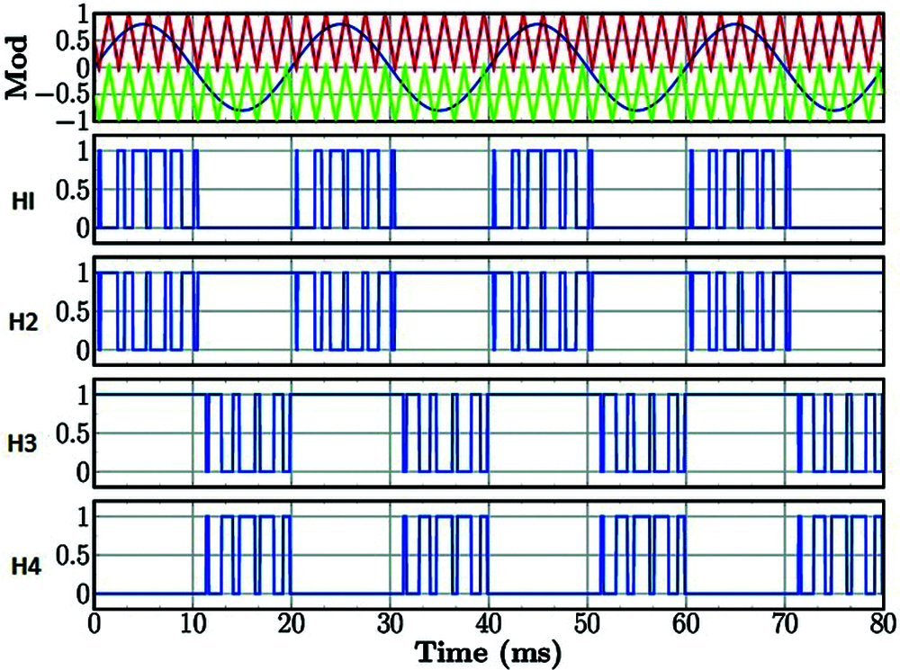
Figure 6: Unipolar POPD PWM
In this proposed work, a unipolar sine and trapezoidal reference with a triangular transporter is utilized to produce terminating beats for a 15 level inverter. For m-level inverter utilizing unipolar multi-bearer systems, (m−1)/2 transporters with a similar recurrence fc and same top to-top plentifulness Ac are utilized. The reference waveform has adequacy Am and recurrence fm and it is put at the zero reference. The reference wave is ceaselessly contrasted and every one of the transporter signals On the off chance that the reference wave is in excess of a bearer signal, at that point the dynamic gadgets comparing to that transporter are turned on.
The proposed PWM is delineated in Figs. 6 and 7. It includes four three-sided transporters and two reference signals (sine wave) for PWM age and the relating simple hardware for base PWM age for each level as depicted in Fig. 7.
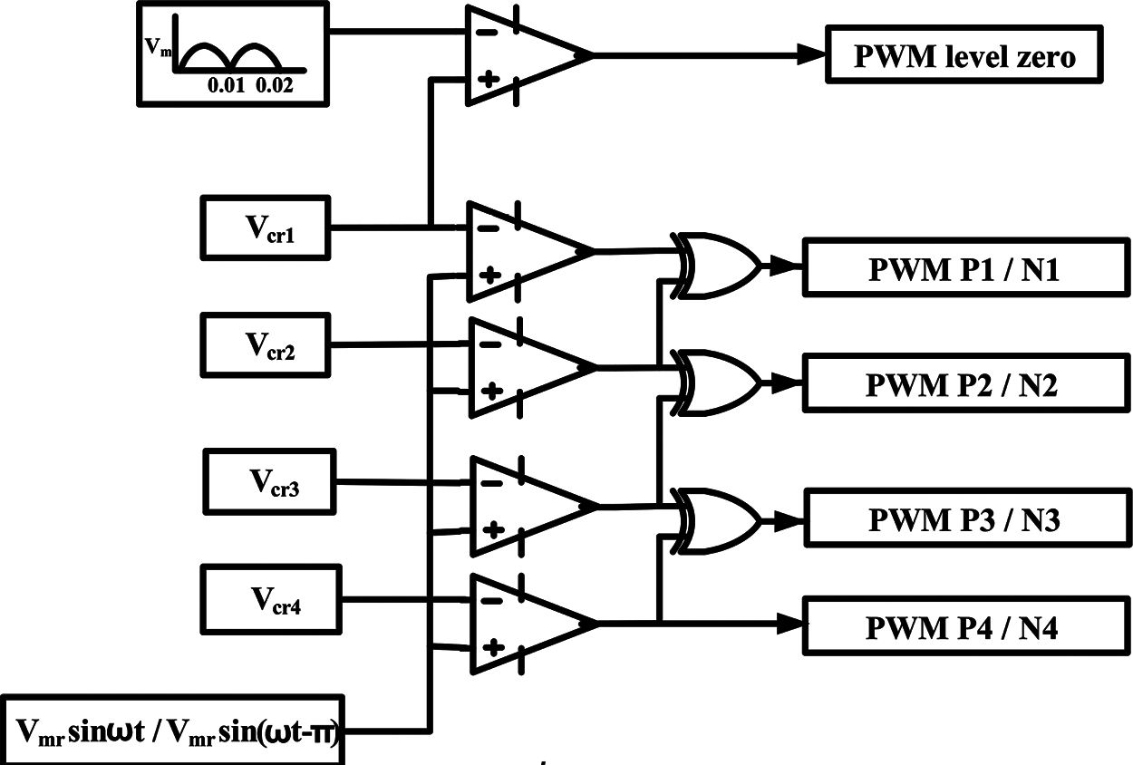
Figure 7: Circuit for PWM generation
The reference wave is consistently contrasted and every one of the transporter signals. On the off chance that the reference wave is in excess of a transporter signal, at that point the dynamic gadgets comparing to that bearer are turned on. Otherwise, the devices are switched off. The frequency of the carrier signal determines the frequency of the AC voltage waveform. And the magnitude of the reference signal determines the effective RMS value of the output voltage waveform.
To validate the proposed method, simulation results summarized in this section have been obtained with a single-phase 15-level CDDCLC using MATLAB/Simulinkenvironment as shown in Figs. 8–10. The simulation conditions are shown in Tab. 2.
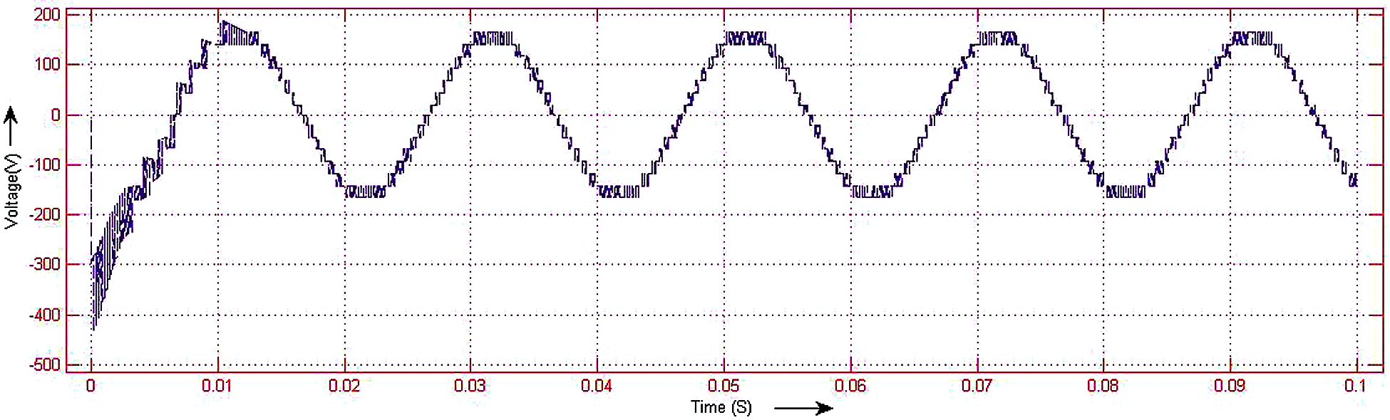
Figure 8: Output (Level generation unit and H bridge) voltage
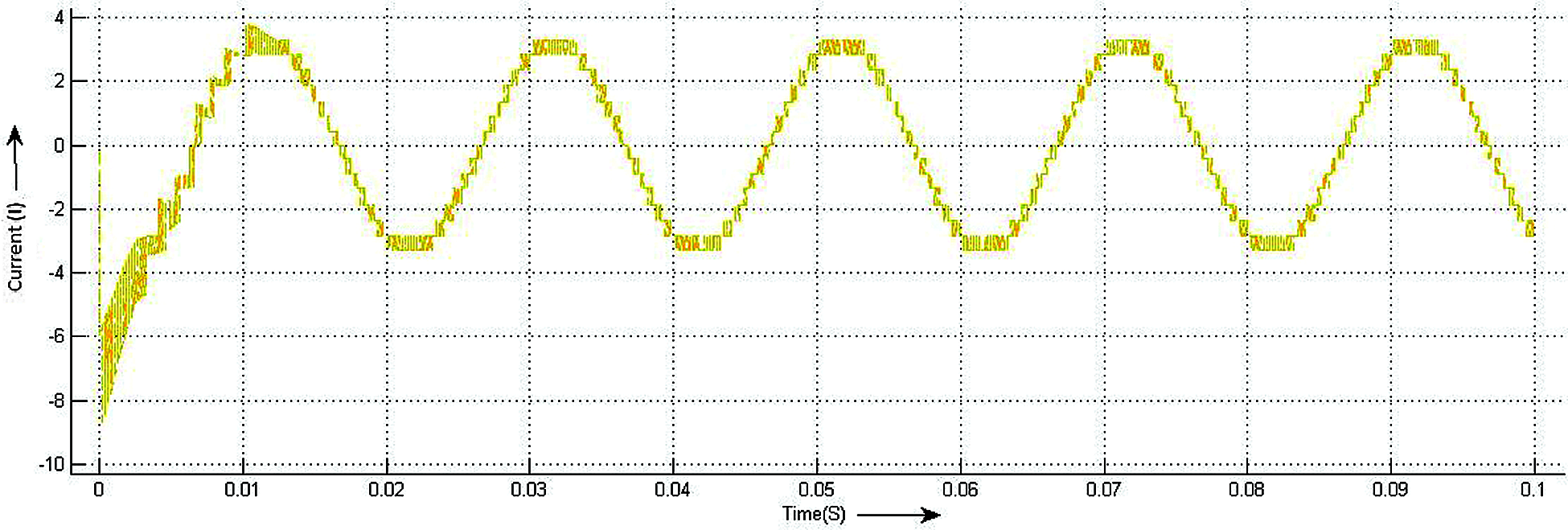
Figure 9: Output (Level generation unit and H bridge) current
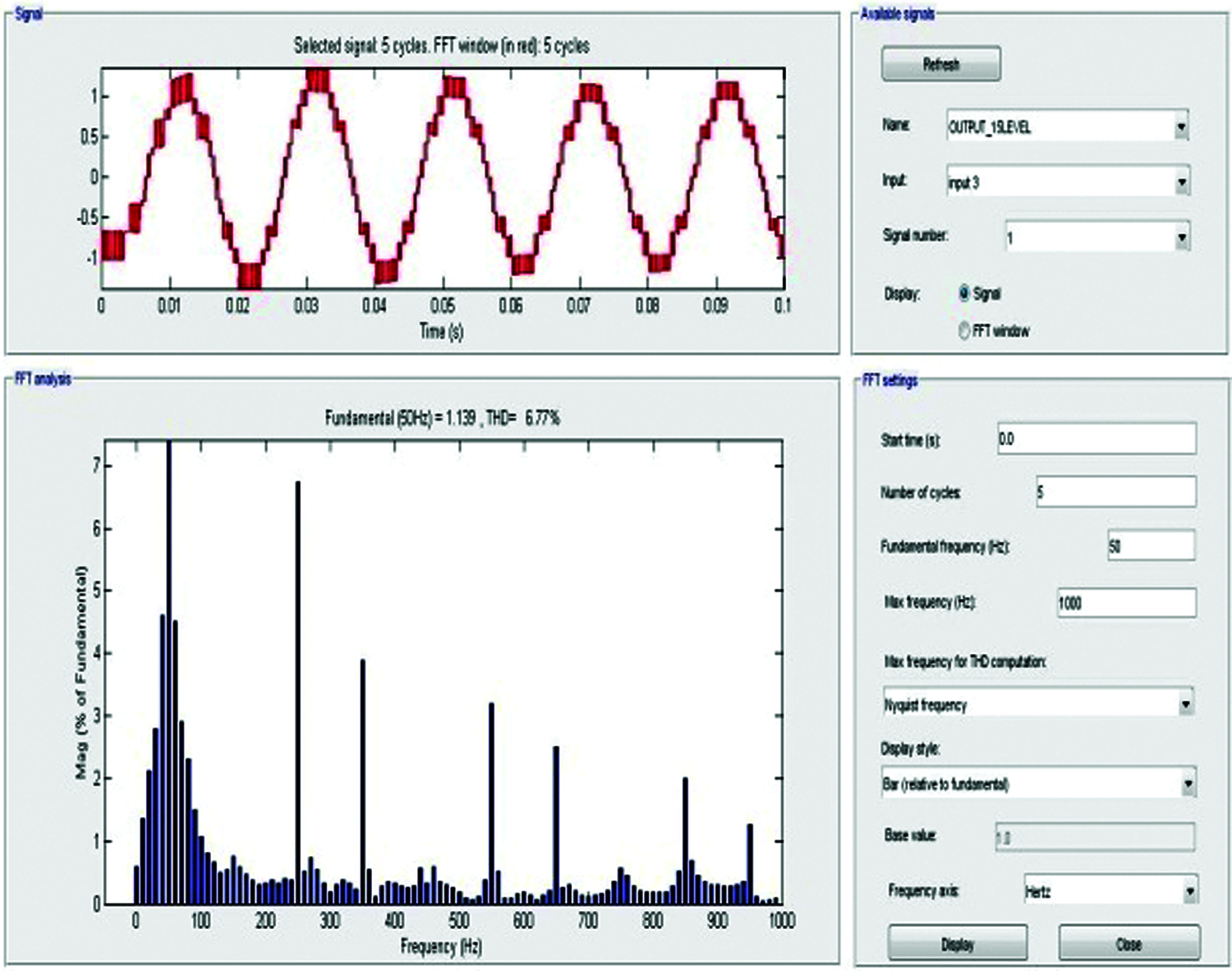
Figure 10: FFT analysis of proposed 15 levels CDDCLC
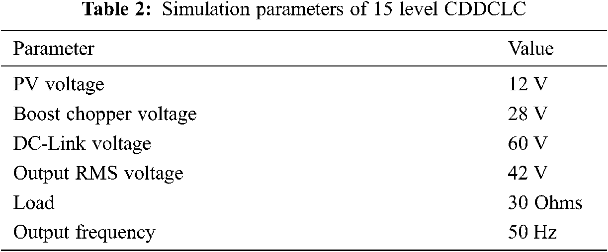
Fig. 8 illustrates the inverter output voltage of level generation unit and the common H Bridge. As a steady-state response, the current waveform for a resistive load is also shown in Fig. 9. In this case, the fs is kHz with the output frequency of 50 Hz.
Simulation results show that the line-to-neutral voltage THD is 6.73% for the proposed 15 level CDDCLC. This confirms the improved power quality of increased output voltage.
6 Comparison of Hardware System Design
A CDDCLC from the DC input to AC output mainly consists of three parts: a chopper, a level generation unit, and common H Bridge. The power loss of the CDDCLC originates from the three parts. The IGBTs are selected for the chopper and multilevel inverter. Most of the power loss in the CDDCLC is due to the switching loss and the conduction loss of the IGBTs and diodes. The 1Ø CDDCLC configuration is intended and applied for 150 V (Vmax) output voltages. It is observed that the Controller and driver unit with CDDCLC constitute the implementation setup. Further, the DC input for the lift chopper units is derived from the supply of rectifier and battery banks. Here, the boost chopper is made up of HGTG20N100D2 insulated gate bipolar transistor (IGBT) switches and passive components (L1 = L2 = 2 mH and C1 = C2 = 100 μF). Tab. 3 represents the technical specifications of HGTG20N100D2 power IGBT and driver ICTLP250. Fig. 11 shows the experimental setup.
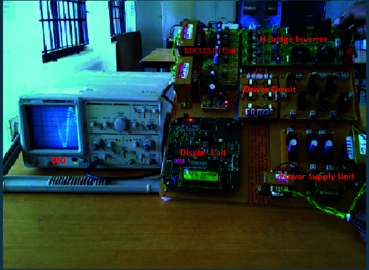
Figure 11: Experimental setup
The control signs to the IGBT driver circuit are given by the microcontroller (ATmega328). The driver circuit is designed using the driver IC from Toshiba-TLP250. HGTG20N100D2 power IGBT switches used in fabricating the DCLM and H-bridge inverter systems. Isolation and amplification processes are provided by the driver circuit using TLP250. Tab. 4 shows the technical specifications of driver IC TLP250.
The hardware results show that the line-to-neutral voltage is 139.9 V as shown in Fig. 12 and the THD is 9.7% as shown in Fig. 13 for the proposed 15 level CDDCLC. It shows the improved power quality performance of output voltage.

Figure 12: Fifteen level Inverter (a) Output voltage & (b) Output current for R Load
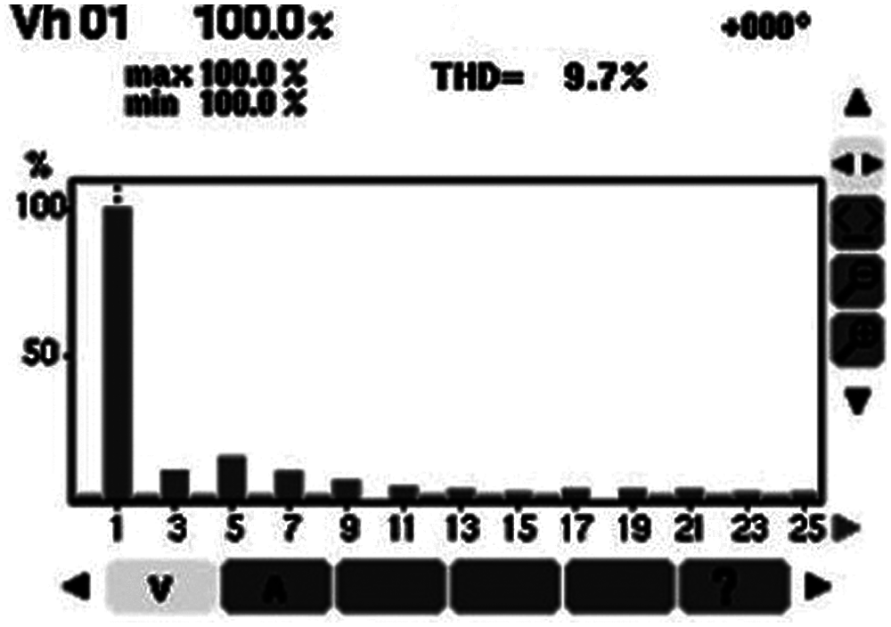
Figure 13: Voltage THD
Fig. 12 illustrates the output voltage and current waveform of inverter circuit with R Load.
Fig. 13 illustrates the Voltage THD harmonic profile for Proposed topology.
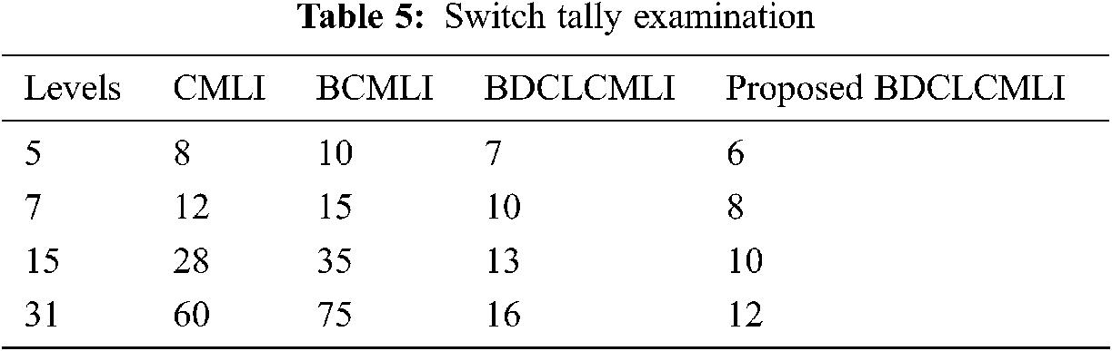
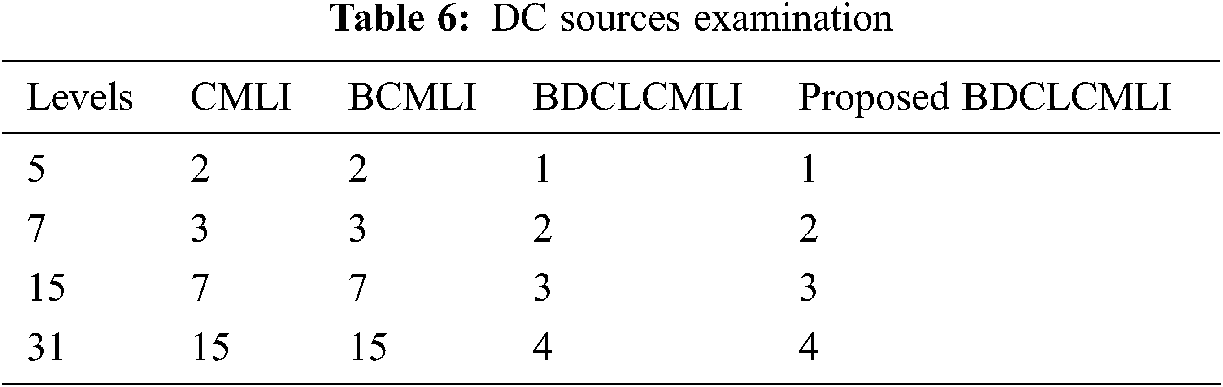
Fig. 14 illustrates the output voltage and current waveform of inverter circuit. The inverter independently generates the desired fifteen level output voltage and current. Tab. 5 shows the correlation of proposed geography with that of other papers mentioned in literature. When compared with other four research papers the work proposed in CDDCLC gives better results. It requires just 10 switches for accomplishing 15 levels. Fig. 16 also shows the qualitative analysis of proposed CDDCLC work. Tab. 6 shows the correlation of proposed geography with that of other papers mentioned in literature. It requires just 3 DC sources for accomplishing 15 levels.
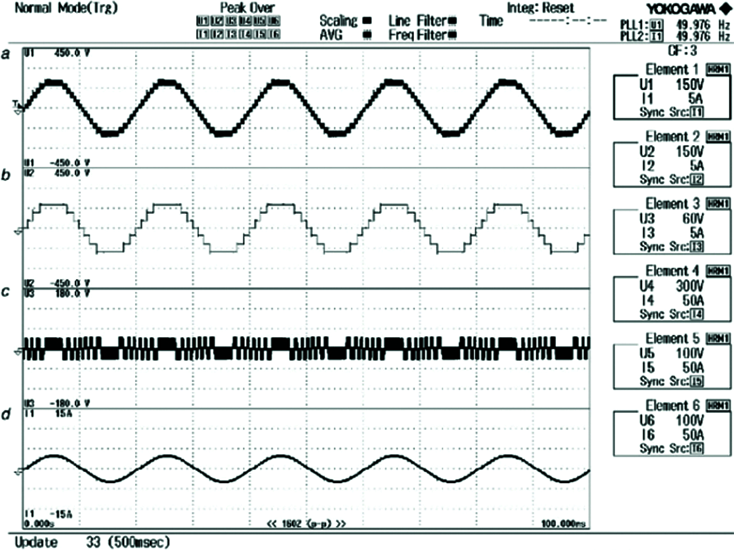
Figure 14: Output voltage and current waveform
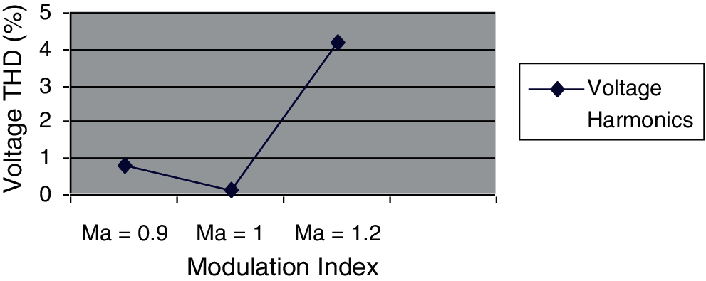
Figure 16: Voltage harmonic analysis of proposed BDCLCMLI (for R Load Vs = 230 V)
Tab. 7 shows simulated harmonic analysis of proposed BDCLCMLI. From the examination voltage harmonics from 8.45%( BDCLCMLI) to 6.73%( Proposed BDCLCMLI). Fig. 15 illustrates the qualitative analysis of proposed BDCLCMLI with other relevant works. The chart demonstrates the improvement of boundaries to be specific number switches, number of sources and voltage stress.
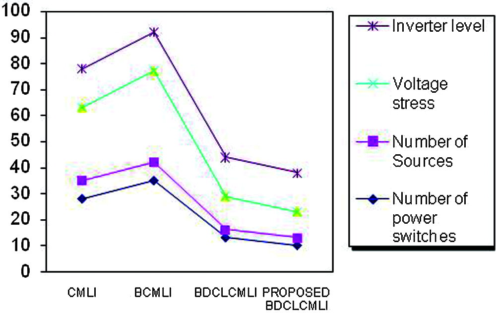
Figure 15: Line chart base qualitative analysis of proposed BDCLCMLI with other works
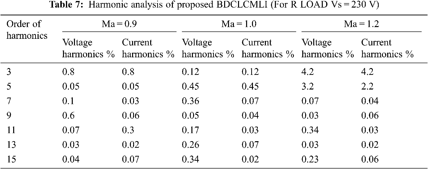
Fig. 16 illustrates the voltage harmonic analysis of proposed BDCLCMLI for R load. The diagram shows the voltage THD for different recurrence adjustment record esteems are investigated.
In this paper single-stage fifteen levels DC-interface converter (CDDCLC) is proposed for sun oriented photovoltaic (PV) applications. The proposed topology is incorporated with support DC chopper and H-connect inverter to optimize the power converter to achieve the minimum harmonic profile. In examination with the traditional inverter frameworks, the proposed framework is utilized with decreased voltage stress, reduced switch check and DC source count. The proposed research work with CDDCLC configuration requires three DC sources for synthesizing fifteen-level AC output. This exploration structure is emphatically suggested for power converters utilized in UPS and drive applications since it is very economical. A reproduction and model of fifteen-level CDDCLC geography shows its total execution. This investigation structure switching technique is phase opposition and disposition pulse width modulation technique (POPD) which results in improved quality of obtained output AC power with 6.73% THD.
Funding Statement: The authors received no specific funding for this study.
Conflicts of Interest: The authors declare that they have no conflicts of interest to report regarding the present study.
1. J. S. Lai and F. Z. Peng, “Multilevel converters-a new breed of power converters,” IEEE Transactions on Industry Applications, vol. 32, no. 3, pp. 509–517, 1996. [Google Scholar]
2. E. E. Espinosa, J. R. Espinoza, P. E. Melín, R. O. Ramírez, F. Villarroel et al., “A new modulation method for a 13-level asymmetric inverter toward minimum THD,” IEEE Transactions on Industry Applications, vol. 50, no. 3, pp. 1924–1933, 2013. [Google Scholar]
3. A. Hota, S. Jain and V. Agarwal, “An improved three-phase five-level inverter topology with reduced number of switching power devices,” IEEE Transactions on Industrial Electronics, vol. 65, no. 4, pp. 3296–3305, 2017. [Google Scholar]
4. Y. Hinago and H. Koizumi, “A single-phase multilevel inverter using switched series/parallel dc voltage sources,” IEEE Transactions on Industrial Electronics, vol. 57, no. 8, pp. 2643–2650, 2009. [Google Scholar]
5. S. Kouro, P. Lezana, M. Angulo and J. Rodriguez, “Multicarrier PWM with DC-link ripple feedforward compensation for multilevel inverters,” IEEE Transactions on Power Electronics, vol. 23, no. 1, pp. 52–59, 2008. [Google Scholar]
6. M. Malinowski, K. Gopakumar, J. Rodriguez and M. A. Perez, “A survey on cascaded multilevel inverters,” IEEE Transactions on Industrial Electronics, vol. 57, no. 7, pp. 2197–2206, 2009. [Google Scholar]
7. S. Rohner, S. Bernet, M. Hiller and R. Sommer, “Modulation, losses, and semiconductor requirements of modular multilevel converters,” IEEE Transactions on Industrial Electronics, vol. 57, no. 8, pp. 2633–2642, 2009. [Google Scholar]
8. I. Colak, E. Kabalci and R. Bayindir, “Review of multilevel voltage source inverter topologies and control schemes,” Energy Conversion and Management, vol. 52, no. 2, pp. 1114–1128, 2011. [Google Scholar]
9. J. Pereda and J. Dixon, “Cascaded multilevel converters: Optimal asymmetries and floating capacitor control,” IEEE Transactions on Industrial Electronics, vol. 60, no. 11, pp. 4784–4793, 2012. [Google Scholar]
10. R. S. Alishah, S. H. Hosseini, E. Babaei and M. Sabahi, “Optimal design of new cascaded switch-ladder multilevel inverter structure,” IEEE Transactions on Industrial Electronics, vol. 64, no. 3, pp. 2072–2080, 2016. [Google Scholar]
11. J. Rodriguez, J. S. Lai and F. Z. Peng, “Multilevel inverters: A survey of topologies, controls, and applications,” IEEE Transactions on Industrial Electronics, vol. 49, no. 4, pp. 724–738, 2002. [Google Scholar]
12. Y. Liu, H. Hong and A. Q. Huang, “Real-time algorithm for minimizing THD in multilevel inverters with unequal or varying voltage steps under staircase modulation,” IEEE Transactions on Industrial Electronics, vol. 56, no. 6, pp. 2249–2258, 2009. [Google Scholar]
13. M. Shen, F. Z. Peng and L. M. Tolbert, “Multilevel DC–DC power conversion system with multiple DC sources,” IEEE Transactions on Power Electronics, vol. 23, no. 1, pp. 420–426, 2008. [Google Scholar]
14. N. A. Rahim and J. Selvaraj,"Multistring five-level inverter with novel PWM control scheme for PV application,” IEEE Transactions on Industrial Electronics, vol. 57, no. 6, pp. 2111–2123, 2009. [Google Scholar]
15. J. Selvaraj and N. A. Rahim, “Multilevel inverter for grid-connected PV system employing digital PI controller,” IEEE Transactions on Industrial Electronics, vol. 56, no. 1, pp. 149–158, 2008. [Google Scholar]
16. R. Uthirasamy, U. Ragupathy, V. K. Chinnaiyan and C. Megha, “Experimentation of boost chopper interfaced cascaded multilevel inverter topology for photo voltaic applications,” Int. Rev. Electr. Eng, vol. 1, no. 9, pp. 16–25, 2014. [Google Scholar]
17. E. Espinosa, J. Espinoza, R. Ramirez, J. Rohten, F. Villarroel et al., “A new modulation technique for 15-level asymmetric inverter operating with minimum THD,” in Proc. IECON 2013, IEEE Industrial Electronics Society, Vienna, Austria, pp. 6164–6169, 2013. [Google Scholar]
18. A. Ajami, M. R. J. Oskuee, M. T. Khosroshahi and A. Mokhberdoran, “Cascade-multi-cell multilevel converter with reduced number of switches,” IET Power Electronics, vol. 7, no. 3, pp. 552–558, 2013. [Google Scholar]
19. M. Miranbeigi, H. Iman-Eini and M. Asoodar, “A new switching strategy for transformer-less back-to-back cascaded H-bridge multilevel converter,” IET Power Electronics, vol. 7, no. 7, pp. 1868–1877, 2014. [Google Scholar]
20. A. Masaoud, H. W. Ping, S. Mekhilef and A. Taallah, “Novel configuration for multilevel DC-link three-phase five-level inverter,” IET Power Electronics, vol. 7, no. 12, pp. 3052–3061, 2014. [Google Scholar]
21. S. Maheswaran, B. K. Paul, M. A. Khalek, S. Chakma, K. Ahmed et al., “Design of tellurite glass based quasi photonic crystal fiber with high nonlinearity,” Optik, vol. 181, pp. 185–190, 2019. [Google Scholar]
 | This work is licensed under a Creative Commons Attribution 4.0 International License, which permits unrestricted use, distribution, and reproduction in any medium, provided the original work is properly cited. |