DOI:10.32604/csse.2022.022386
| Computer Systems Science & Engineering DOI:10.32604/csse.2022.022386 | |
| Article |
Efficient Supply Current Control Strategies for Bridgeless Interleaved AC-DC Converter
1Department of Electrical and Electronics Engineering, Sathyabama Institute of Science and Technology (Deemed to be University), Chennai, Tamil Nadu, 600119, India
2Department of Electrical and Electronics Engineering, SSN College of Engineering, Chennai, Tamil Nadu, 603110, India
*Corresponding Author: R. Sasikala. Email: r.sasikala.phd@gmail.com
Received: 05 August 2021; Accepted: 29 October 2021
Abstract: This paper presents an efficient supply current wave shaping technique for bridgeless interleaved Single Ended Primary Inductor Converter (SEPIC). The SEPIC converter converts an Alternating Current (AC) to Direct Current (DC) with the boost converter. Power Factor Correction (PFC) is progressively significant to achieve high energy efficiency. The overall system efficiency can be increased as the bridgeless topology has less conduction losses from rectifying bridges. Also, the bridgeless and interleaved techniques are incorporated in this study to achieve better performance. The performance of the system is analyzed on both current control and sensor-less techniques. Different controllers such as Proportional Integral (PI) control, peak current control, Non-Linear Carrier (NLC) control, and sensor-less current control are integrated. All the above controllers are implemented using MATrix LABoratory (MATLAB)/SIMULINK. The performance parameter, namely Power Factor (PF), Total Harmonic Distortion (THD), is computed for both open loop and closed loop condition. The sensor-less current control method is implemented using the DsPIC30F2010 controller. The circuit performance is also verified from the simulation and hardware results. The proposed controller has inbuilt Analog-to-Digital Converter (ADC), Digital-to-Analog Converter (DAC), Pulse Width Modulation (PWM) generator, and provides fast responses.
Keywords: Light emitting diode; power factor correction; SEPIC converter; current control method; sensor-less method; fast Fourier transform analysis for input current
Light Emitting Diode (LED) becomes the most eco-friendly and fashionable light source due to its advantages such as highlight efficacy, long lifetime, high reliability, low maintenance requirements, small sizes and harm-free than other light sources [1]. The LEDs are used in many domains such as street lighting, traffic lighting, automotive lighting and decorative lighting system [2]. Since the demand of the LEDs is increased in both industrial and commercial applications, it requires a high reliable power supply. The conventional AC to DC power converter has limitations such as poor input PF and increased supply current harmonic [3]. To overcome these limitations, single-stage and two-stage methods are designed for active methods.
Two-stage methods have an additional converter such as boost, buck, and buck-boost converter that improve the input PF [4]. This two-stage AC to DC converter increases the cost, size, and reduces the system efficiency. Many single-stage AC to DC converters are designed for regulating the input current harmonics and PF. The integrated buck-boost converter with a buck converter is discussed in [5] for single-stage PFC correction. It has two active switches which increases the control complexity. The integrated double buck converter is designed in [5] for single-stage PFC correction. It suffers from zero-crossing distortion in input current and requires floating driver circuit [5].
The bridgeless topology in SEPIC Converter is implemented in [6] instead of integrating two converters which better PF and reduces harmonics also. In the conventional bridgeless SEPIC converter, only one semiconductor device will be in conduction at a time so that the conduction loss can be reduced which in turn increases the overall efficiency of the system. In addition to the bridgeless topology interleaved technique is added to the SEPIC converter in [7]. The interleaved circuit is able to process more power with reduced circuit ripples, harmonic distortion and current stresses.
In the conventional PFC techniques, the resistive sensor is normally used for sensing the current which is more costly and creates huge problems in the circuit due to the heating and power loss. Instead of using resistive sensor, the use of digital control method requires the voltage across the resistor to be converted into digital format using ADC and the frequency of the supply current should match with the switching frequency. Thus, the ADC used for sensing the supply current should have higher sampling frequency than the ADCs used for the input and output voltages which change at the line frequency and can be low cost ADCs. Numerous PFC control algorithms are available by the use of current sensor less control. In [8], PF correction based on digital current rebuilding is achieved. The computational cost is high and also the supply current has a distorted waveform and is not perfectly in phase with the input voltage. In [9], a current-sensor less digital controller for active PFC based on Kalman filters is designed. It also has high computational cost and the input current waveform is not nearly a sinusoidal waveform [9].
In this paper, interleaved bridgeless SEPIC converter is proposed based on the current control technique along with current sensor less technique. Also, a comparative study is made using the following parameters; supply current THD and PF [10]. Two current control techniques; peak current control technique and NLC control techniques are implemented. In the current sensor less method, current sensor is not used directly in the circuit so that the total cost of the system is reduced. For sensing the supply and load voltage, ADCs are used which make the system reliable when compared to other methods [11]. For the current wave shaping and to make the proposed technique more accurate than other techniques, especially in the transient operations, a Zero-Crossing Detector (ZCD) is connected in the circuit which gives perfect result even in the transient conditions. The input current has a sinusoidal waveform when using distorted supply voltage.
2 Interleaved Bridgeless SEPIC Converter
The SEPIC is a type of DC/DC converter that enables electric power (voltage) at its output to be higher than, lower or equal to that on its input. The SEPIC output is regulated by the control switch’s operating cycle. The SEPIC interleaved functions are operated in two modes; continuous and discontinuous modes. The output voltage of the interleaved SEPIC exceeds or equivalents to the input voltage. The interleaved technique reduces the switching stress of the converter and also improves the efficiency. PFC-boost bridgeless design decreases the conduction loss by failing to use the rectifying bridge and enhances the efficiency. The advantages of this converter are decreased driving loss, less equipment and high performance.
The interleaved bridgeless SEPIC converter is shown in Fig. 1. Both bridgeless and interleaved concepts are added in the modified circuit for the wave shaping technique in [12]. The modified circuit consists of two additional diodes and Metal Oxide Semiconductor Field Effect Transistor (MOSFET) switches than the normal conventional bridged rectifier circuit. This configuration gives high efficacy due to low conduction losses and reduces THD with improved supply current PF. This circuit has two modes of operation. During the positive half cycle, switches Q1 and Q3 are on at that time, the L1 and L3 are get charging, and L2 and L4 are discharging the energy through capacitor C2 and C4 via body diode of Q4/Q2 switches and deliver to the load. During the negative half cycle, switches Q2 and Q4 are on at that time, the L2 and L4 are get charging, and L1 and L3 are discharging the energy through capacitor C1 and C3 via body diode of Q1/Q3 switches and delivers to the load [13].
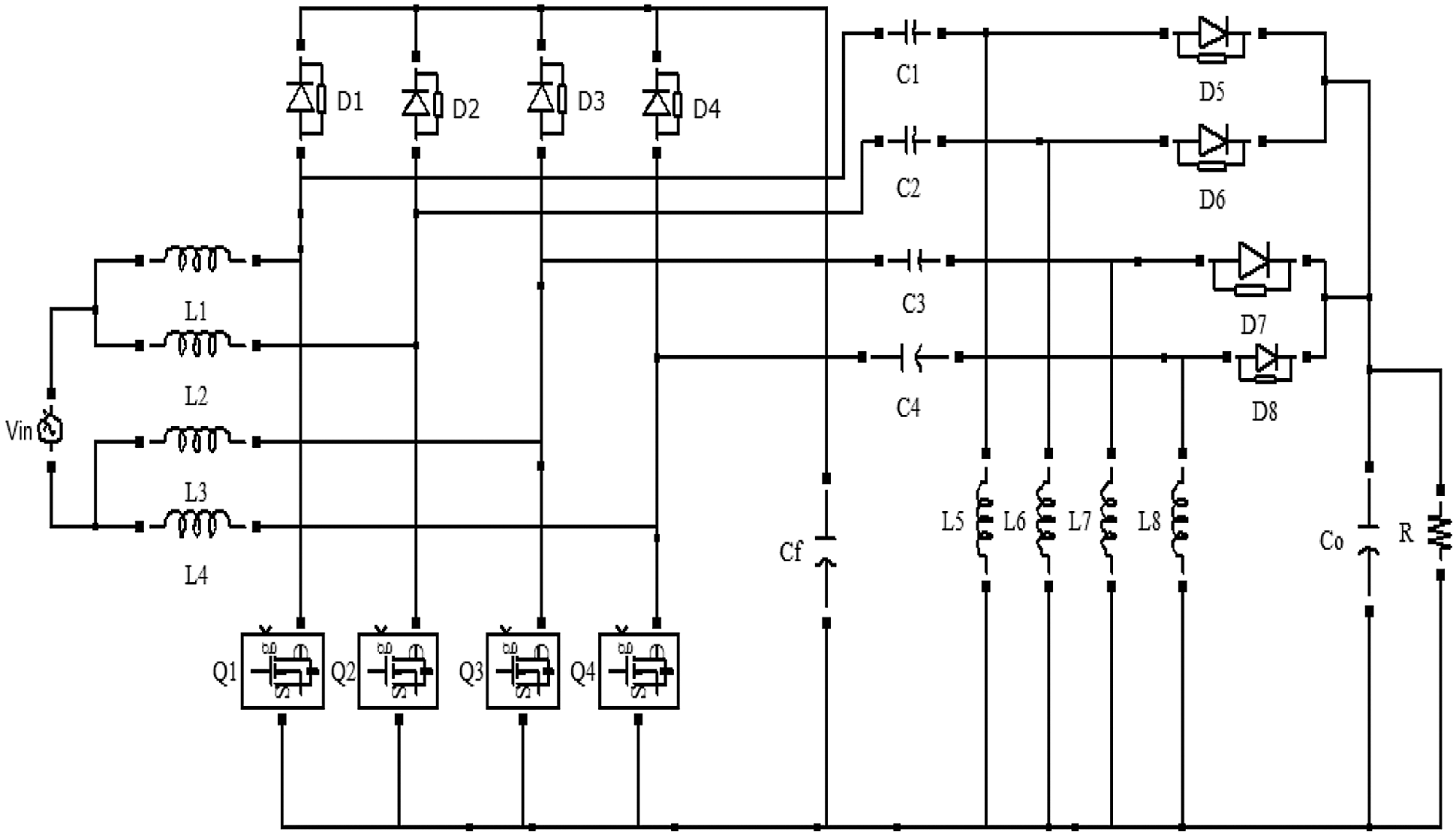
Figure 1: Interleaved bridgeless SEPIC converter circuit diagram
The design equations for the proposed converter are as follows:
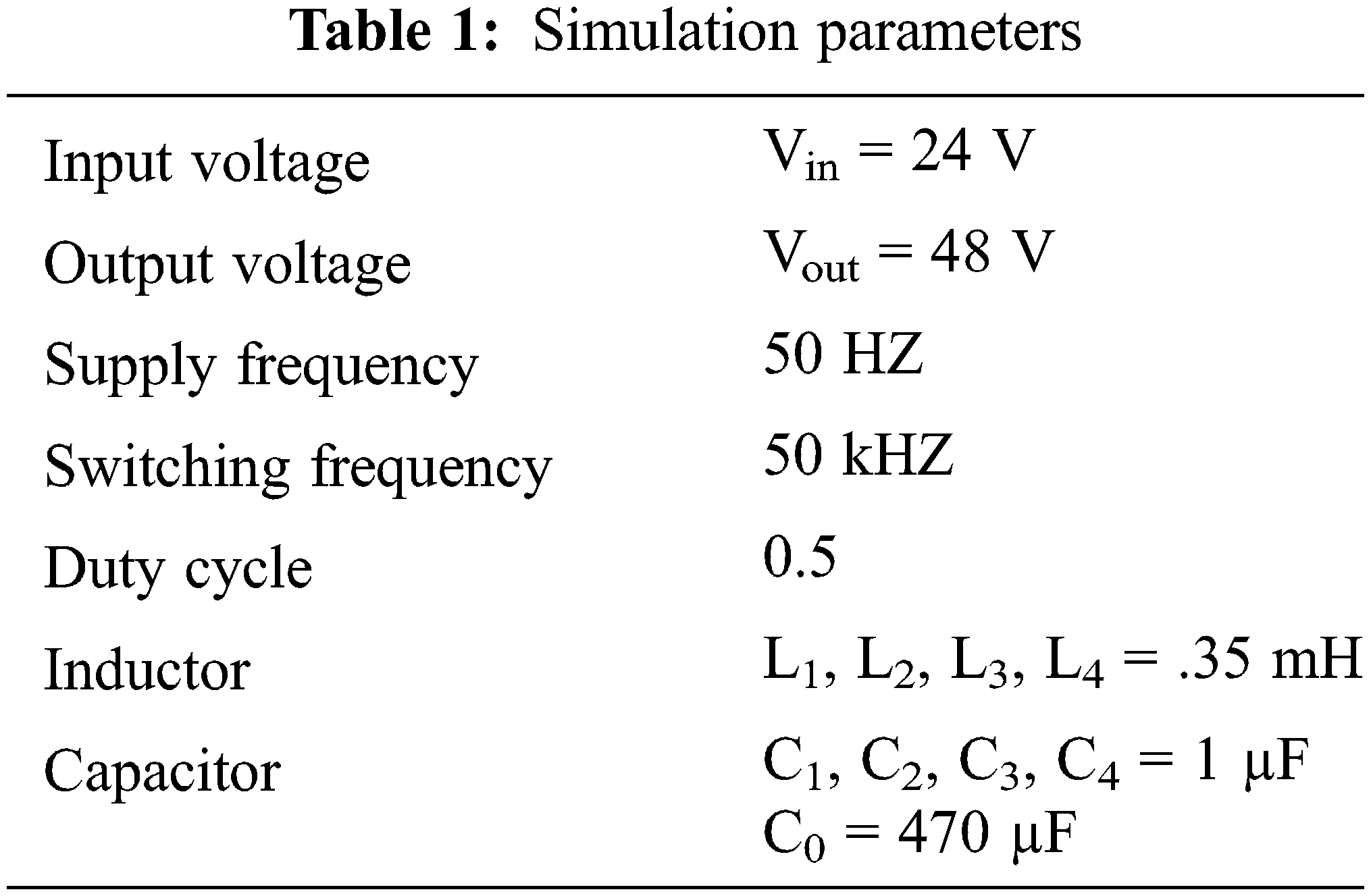
The components are designed using the above mentioned Eqs. (1)–(5) and the computed parameters are tabulated in Tab. 1.
3 Current Control Strategies for the Proposed Topology
The main drawback of the AC to DC PFC converters is poor input PF and increased current harmonics. The closed loop control is implemented to shape the supply current by taking feedback from the source and load side [14]. The inner control loop is used to control the PF and to reduce the harmonics and the outer loop is used to regulate the output voltage. Various supply current wave shaping methods are discussed in the literature [15]. In this work, the control method such as PI controller, peak current controller, NLC controller, and sensor-less current control method are presented and compared.
Fig. 2 shows the circuit diagram of interleaved bridgeless SEPIC converter with the PI controller. The PI controllers adjust the proportional gain (Kp) and the integral gain (Ki) value according to the error signal and regulate the output voltage. The final adjusted values of Kp and Ki are 1, 0.5 respectively. Though it is a simple and low cost method, the input side parameters are not considered for regulating the output voltage and control the input PF [16].
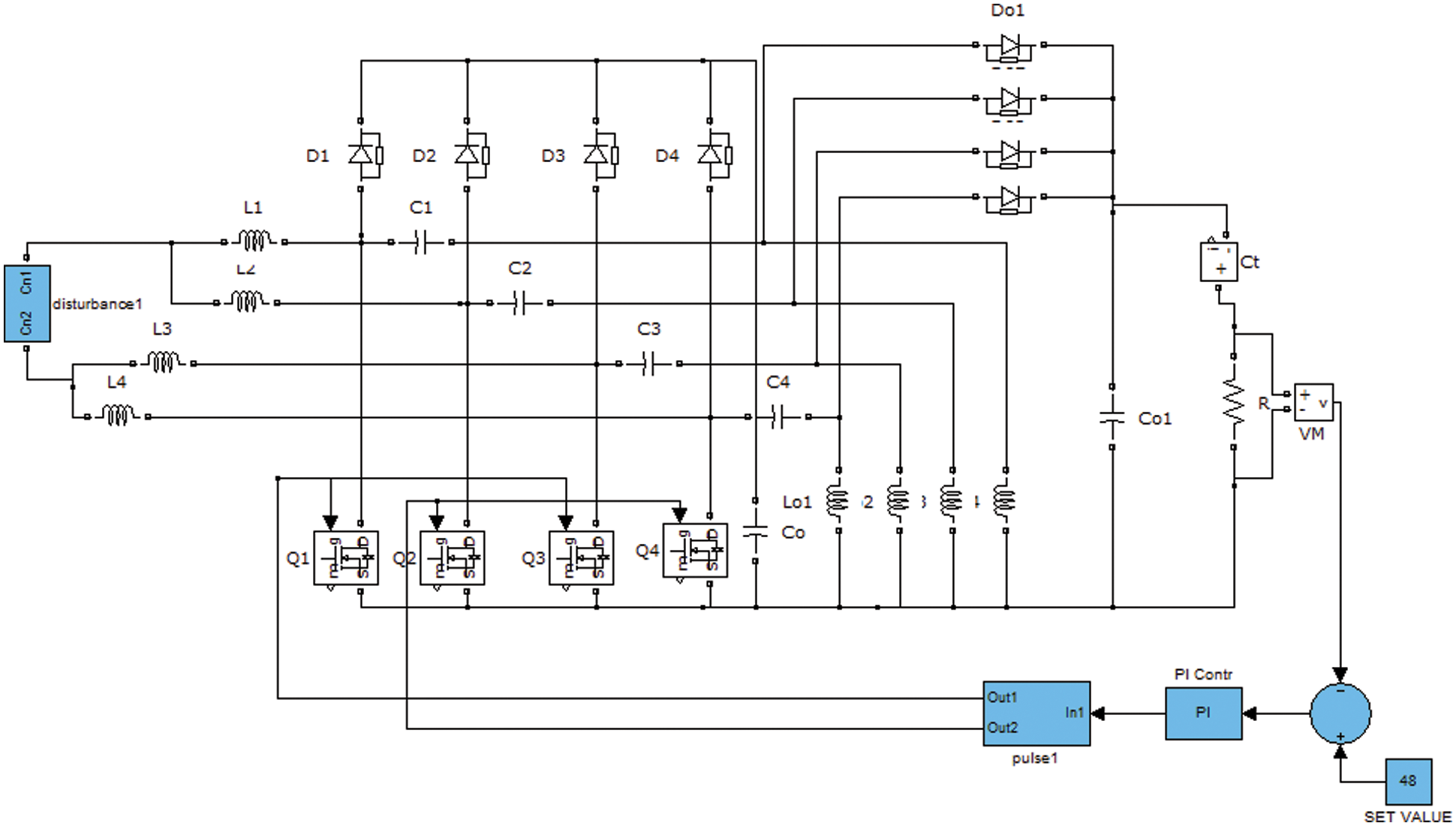
Figure 2: Interleaved bridgeless SEPIC converter with PI controller
3.2 Peak Current Control Method
Fig. 3 shows the interleaved bridgeless SEPIC converter with peak current controller. In this circuit, the measured output voltage is taken as a reference signal-1 and the measured input current is converted into equivalent voltage which is taken as a reference signal-2. These two reference signals are multiplied and compared with input inductor current. This signal difference is called as an error signal. It is given to the flip flop circuit. A flip-flop or latch in electronics is a two-stable circuit, which is suitable for storing state information. It is an artificial multi vibrator.
The circuit may be created to modify the state of signals for one or more input controls and has one or two outputs. The flip flop circuit generates the PWM pulses and regulates the output voltage. This method also does not consider the input side parameters for regulating the output voltage and control the input PF. This controller has the following advantages; cycle-by-cycle current limiting, a simple feedback compensation network, and inherent short circuit protection.
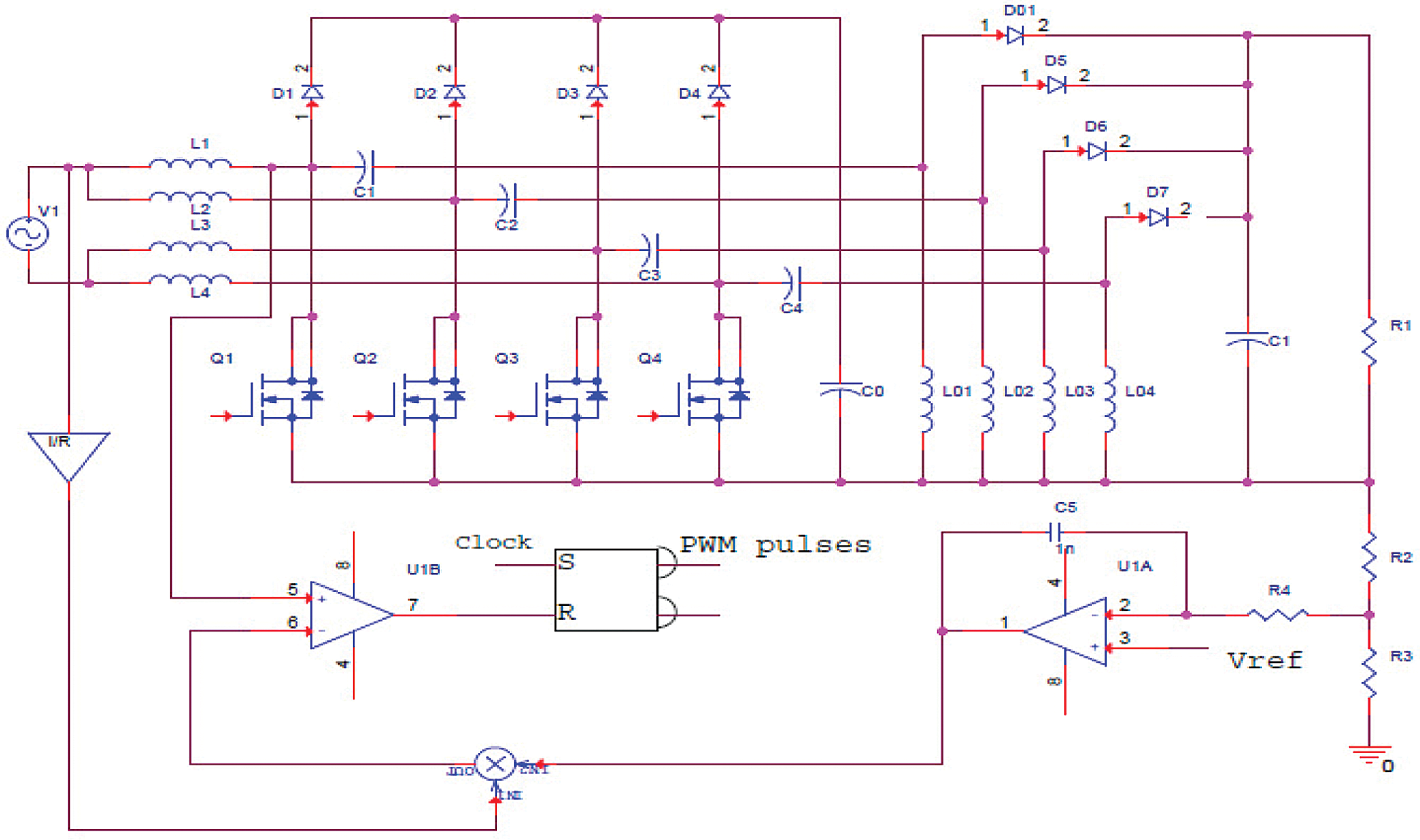
Figure 3: Interleaved bridgeless SEPIC converter with peak current controller
3.3 Non-Linear Carrier Control
Generating the periodic carrier waveform is the main component of the NLC control. Fig. 4 shows the interleaved bridgeless SEPIC converter with non-linear carrier current controller. The waveform generator can be built with the same technique as the NLC. The NLC with the highest current has the same benefits as the NLC. In this way, a negative waveform is produced from the output voltage in comparison with the reference voltage.
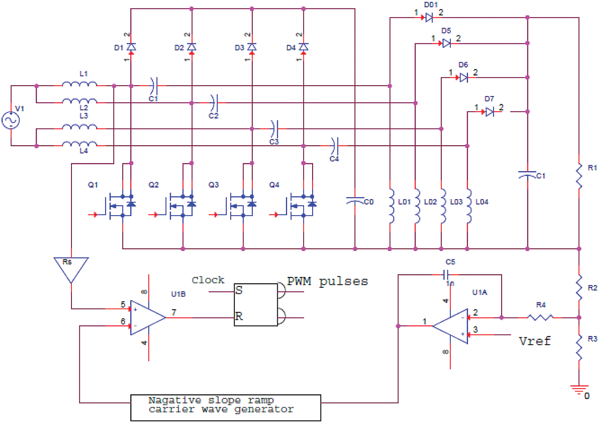
Figure 4: Interleaved bridgeless SEPIC converter with non-linear carrier current controller
The controller uses switch-current sensing that do not need a current-sensing amplifier, no input voltage sensing, and no voltage feedback multipliers/dividers. In this case, the service cycle is regulated in two ways: through the sensor electricity and through the sensing of the switch. The duty ratio is calculated by comparing the periodic NLC waveform with a signal derived from the primary switch current.
3.4 Sensor-Less Control Method
Fig. 5 shows the sensor-less current controller functional diagram. The inductor current can be obtained without using a current sensor and it depends on the sensed input and output voltage. The output voltage Vo(t) is given to the ADC and the output of the ADC is given to the comparator which compares the output voltage to Vref (48 V) and generates the error signal (Verror). The error signal (Verror), which gives the first Iref signal, is provided as an input to the PI controller. A ZCD is used to detect the sine waveform transition from positive and negative and provides signal when the zero voltage is crossed. The phase metre and time indicator generator are designed by using ZCD. The lookup table is used to generate the second (Isin) signal from the input voltage and these signals are multiplied and compared to generate other reference signals.
The PWM pulse output is generated using a hysteresis band gap according to the error signal. In order to ensure the exact control during transit, the ZCD is used by the sensor-less current technique. Thus, this approach has a simple control mechanism than other control techniques. The inherent instantaneous over-current safety for the power switch has an additional benefit. However, the NLC has a simpler waveform generator and enables a greater tolerance to noise due to the integration of the sensed switch current.
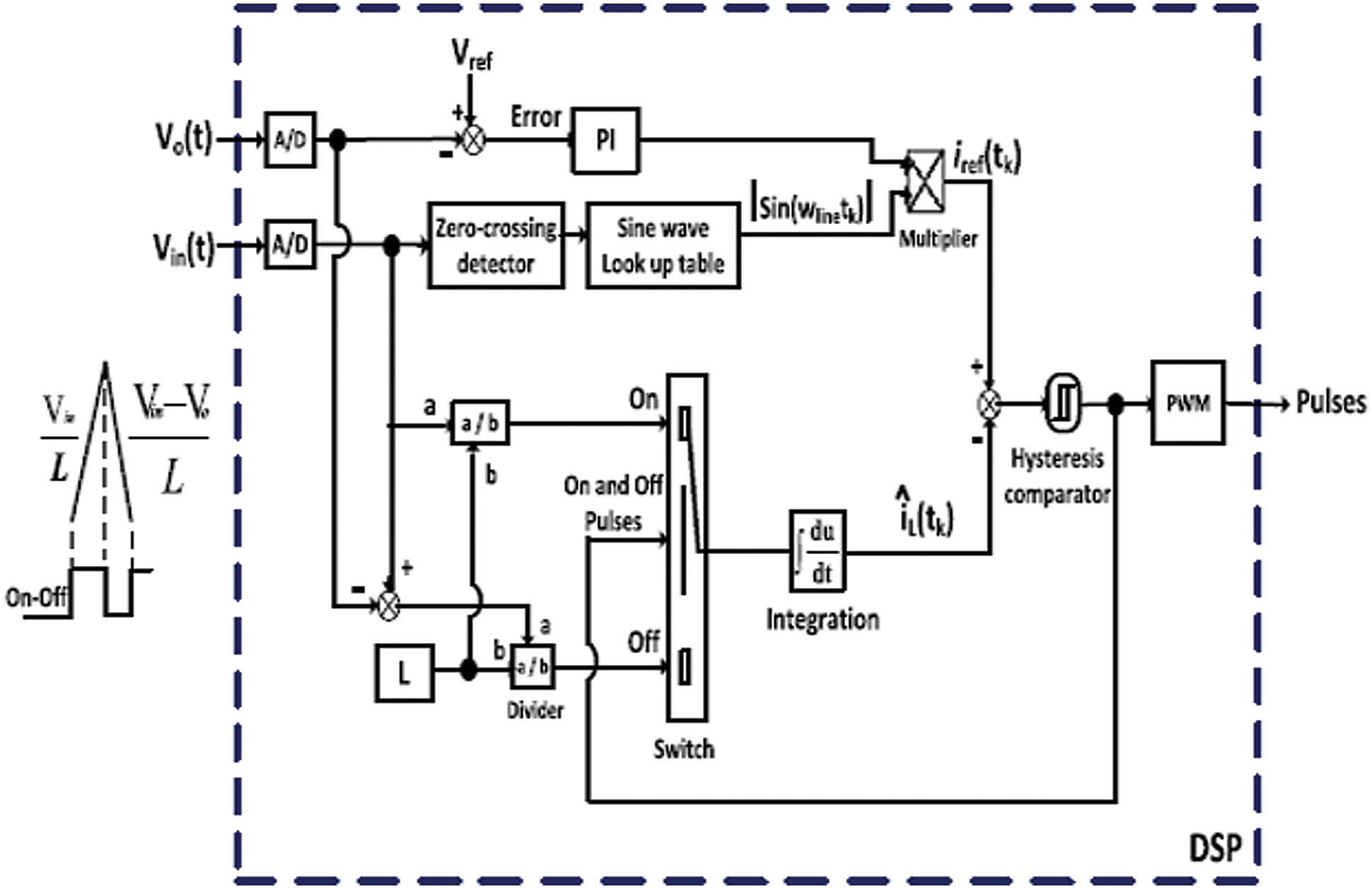
Figure 5: Proposed control technique without using the current sensor
The proposed circuit is simulated using MATLAB/SIMULINK. Tab. 2 shows the parameters chosen for the AC to DC converter.
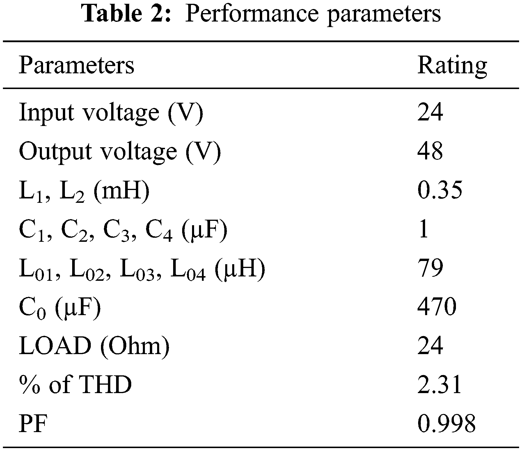
Fig. 6 shows the output voltage at a fixed duty cycle.
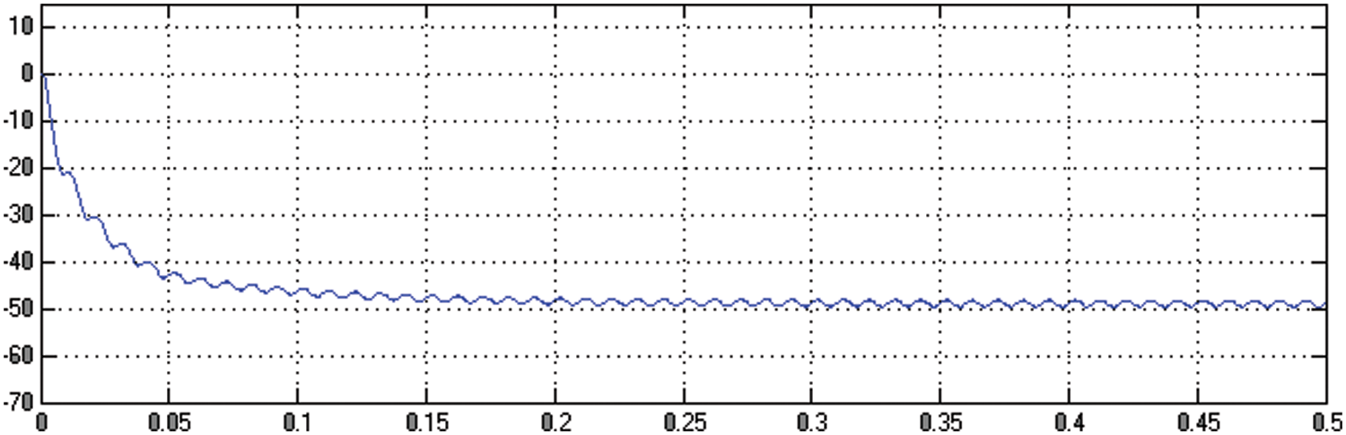
Figure 6: Output voltage waveform
Fig. 7 shows the input voltage and the current waveform.
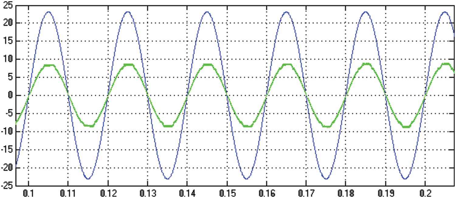
Figure 7: Input voltage and current waveform
Fig. 8 shows the FFT analysis for the input current. The input current has a THD of 6.24%.
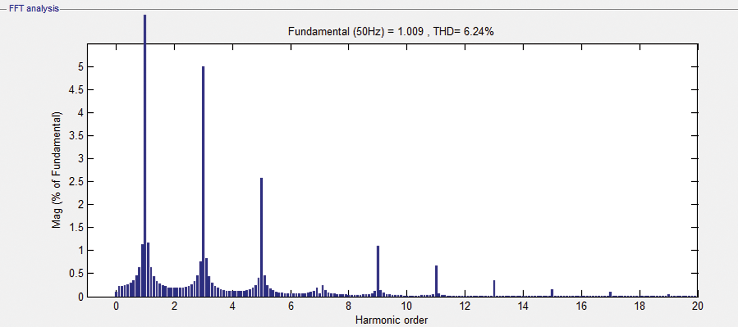
Figure 8: FFT analyses for current waveform
The performance of the proposed sensor-less current control method is analyzed with three different current control techniques such as PI control method, peak current control method, and average current control method.
Fig. 9 shows the output voltage for the PI controller.
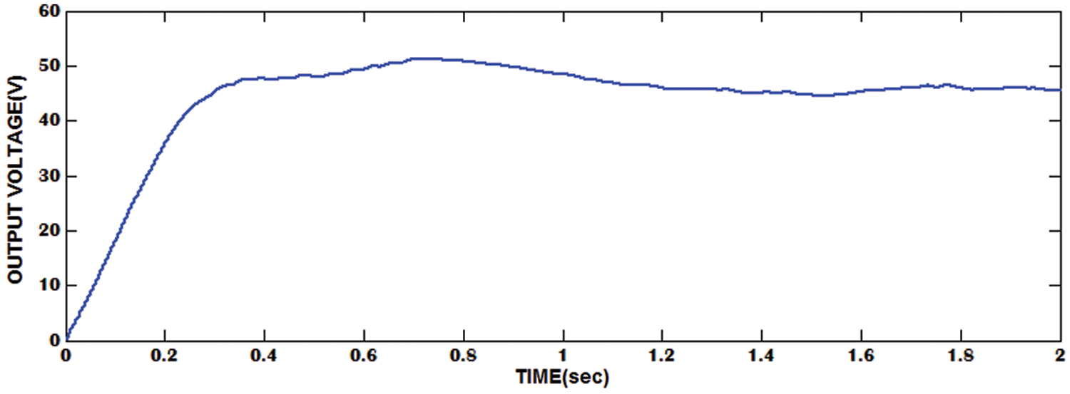
Figure 9: Output voltage waveform
Fig. 10 shows the input voltage and current waveform for the PI controller.
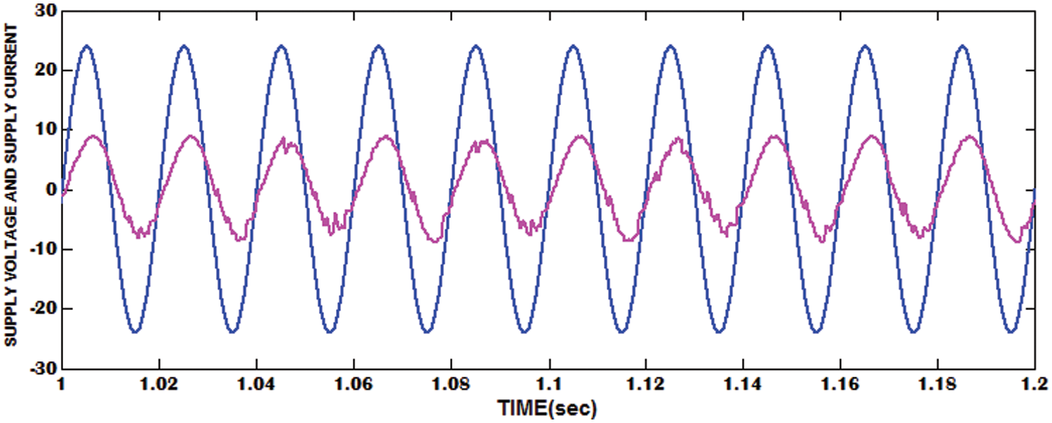
Figure 10: Input voltage and current waveform
Fig. 11 shows the FFT analysis for current. The input current has a THD of 26.95%.
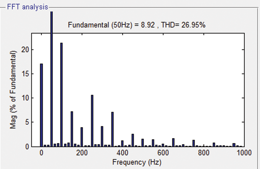
Figure 11: FFT for supply current waveform
Fig. 12 shows the output voltage for the peak current controller.
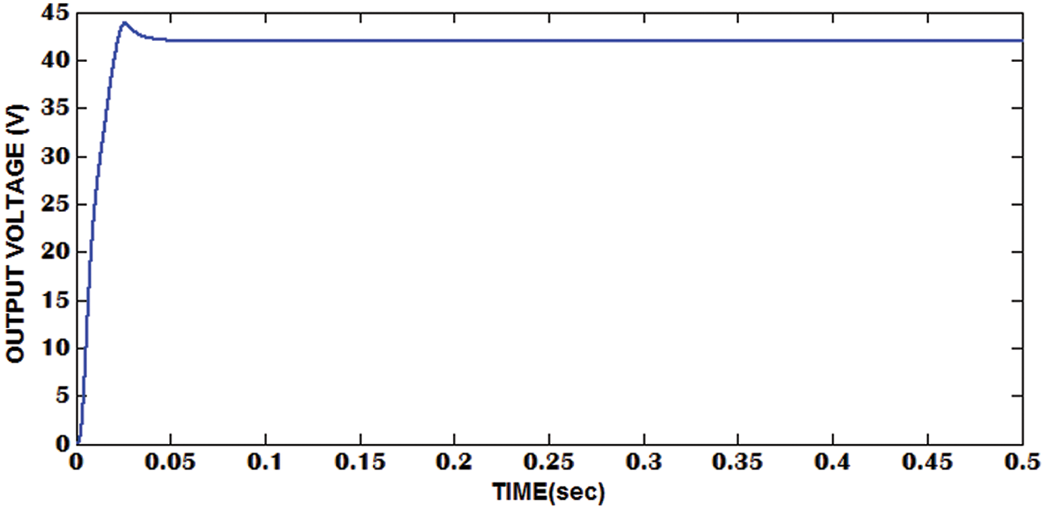
Figure 12: Output voltage waveform
Fig. 13 shows the input voltage and current waveform for the peak current controller.
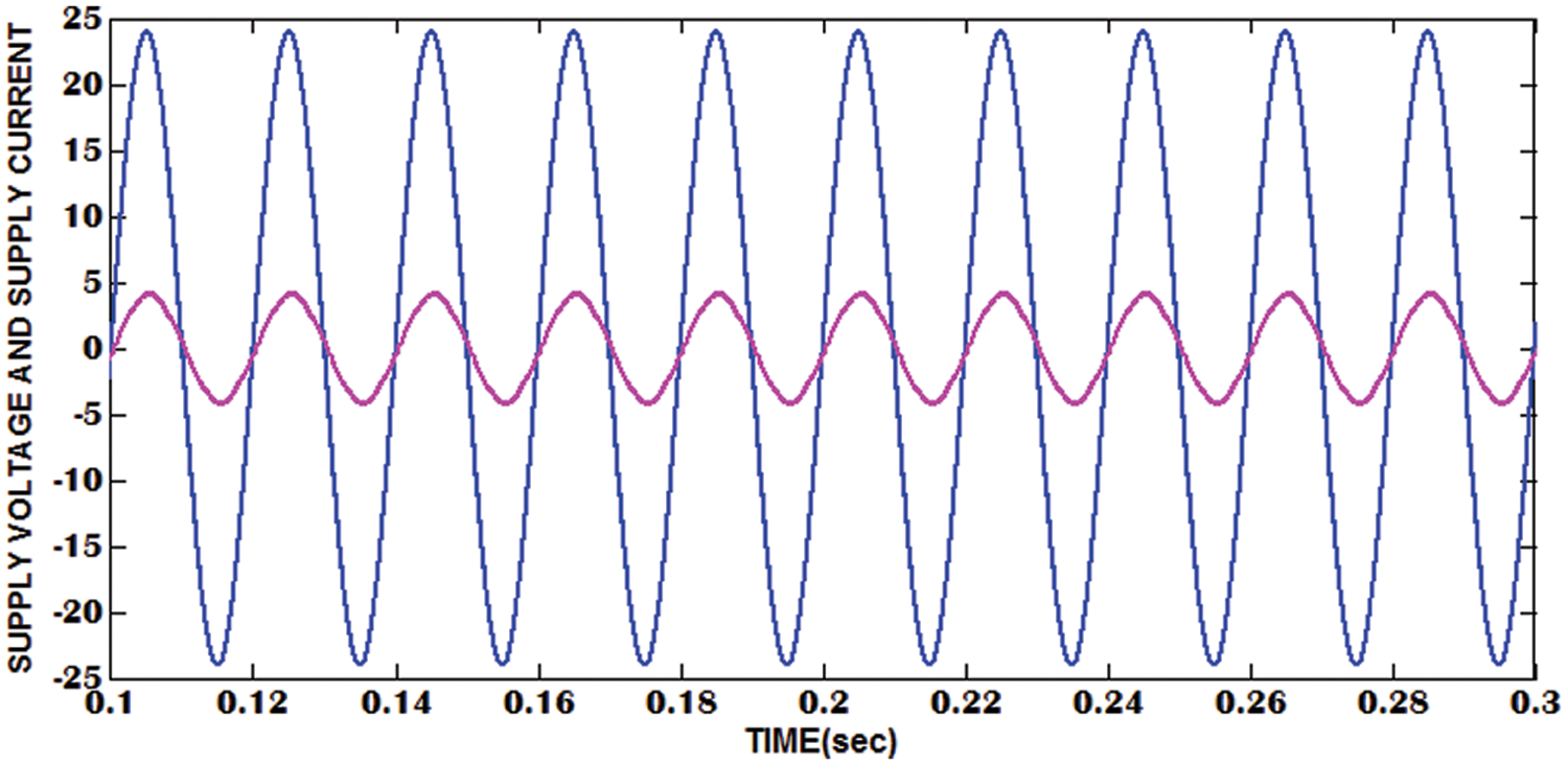
Figure 13: Input voltage and current waveform
Fig. 14 shows the FFT analysis for input current. The input current has a THD of 10.16%.
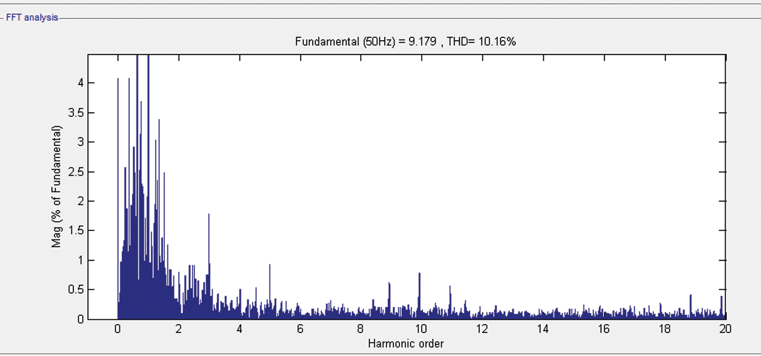
Figure 14: FFT analyses for current waveform
Fig. 15 shows the output voltage for the NLC controller.

Figure 15: Output voltage waveform
Fig. 16 shows the input voltage and current waveform for NLC controller.
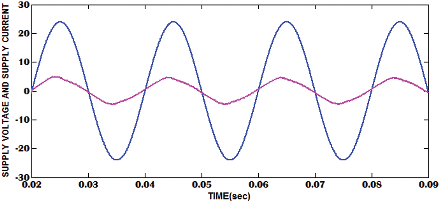
Figure 16: Input voltage and current waveform
Fig. 17 shows the FFT analysis for input current. The input current has a THD of 6.33%.
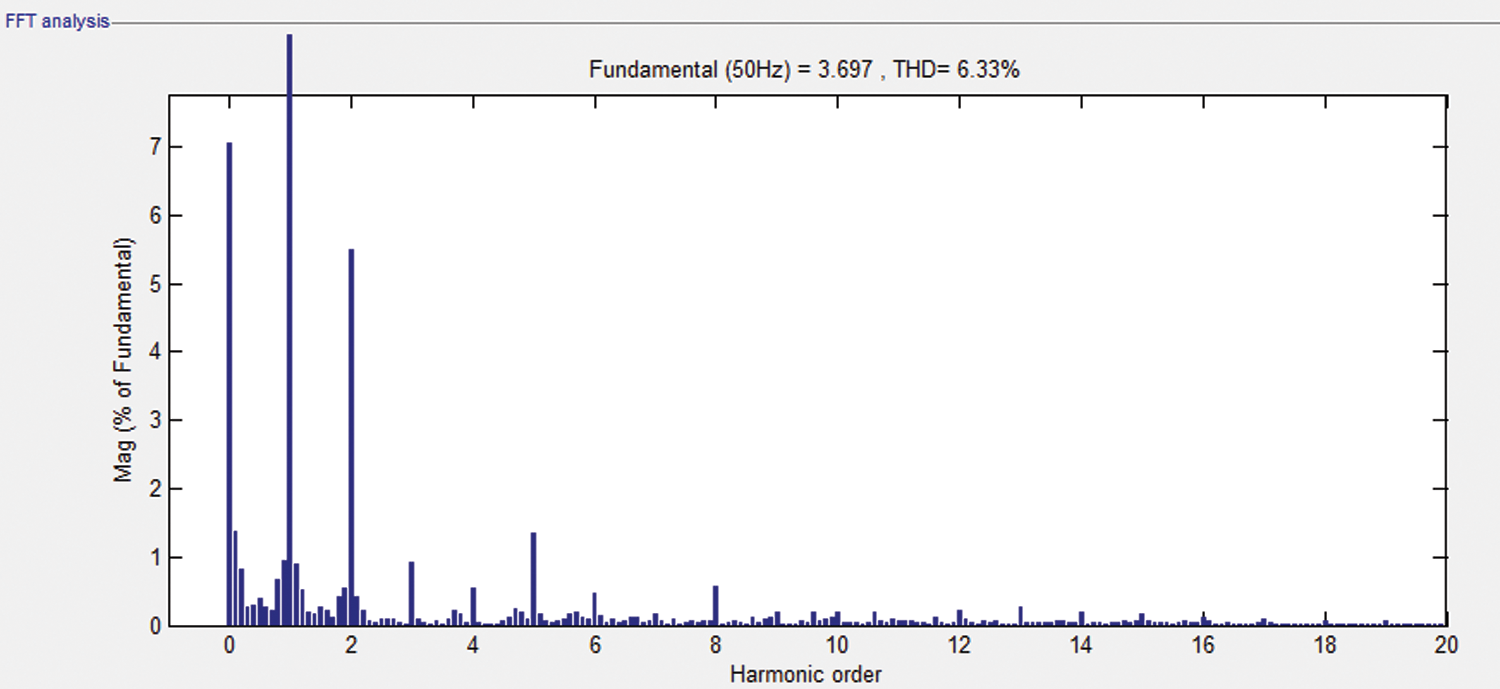
Figure 17: FFT analyses for current waveform
4.2.4 Sensor-Less Current Controller
Fig. 18 shows the output voltage from the sensor-less current controller.
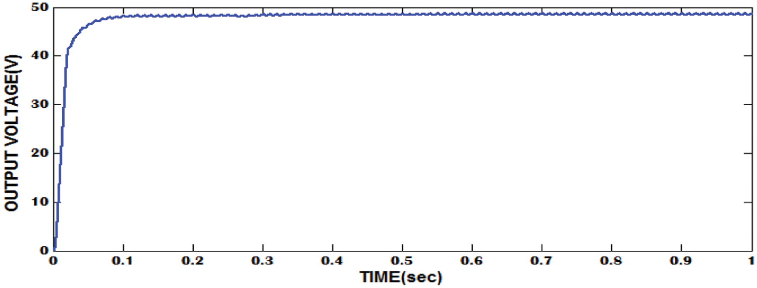
Figure 18: Output voltage waveform
Fig. 19 shows the input voltage and current waveform from the sensor-less current controller. Both input current and voltage waveform cross the zero point at the same time. Due to this the input current follows the sinusoidal shape and has fewer harmonics.
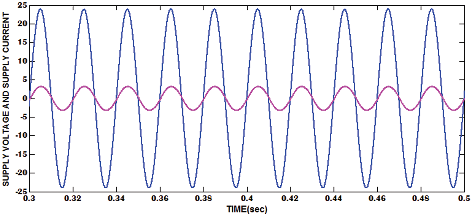
Figure 19: Input voltage and current waveform
Fig. 20 shows the FFT analysis for input current of sensor-less current controller. The input current has a THD of 2.31%.
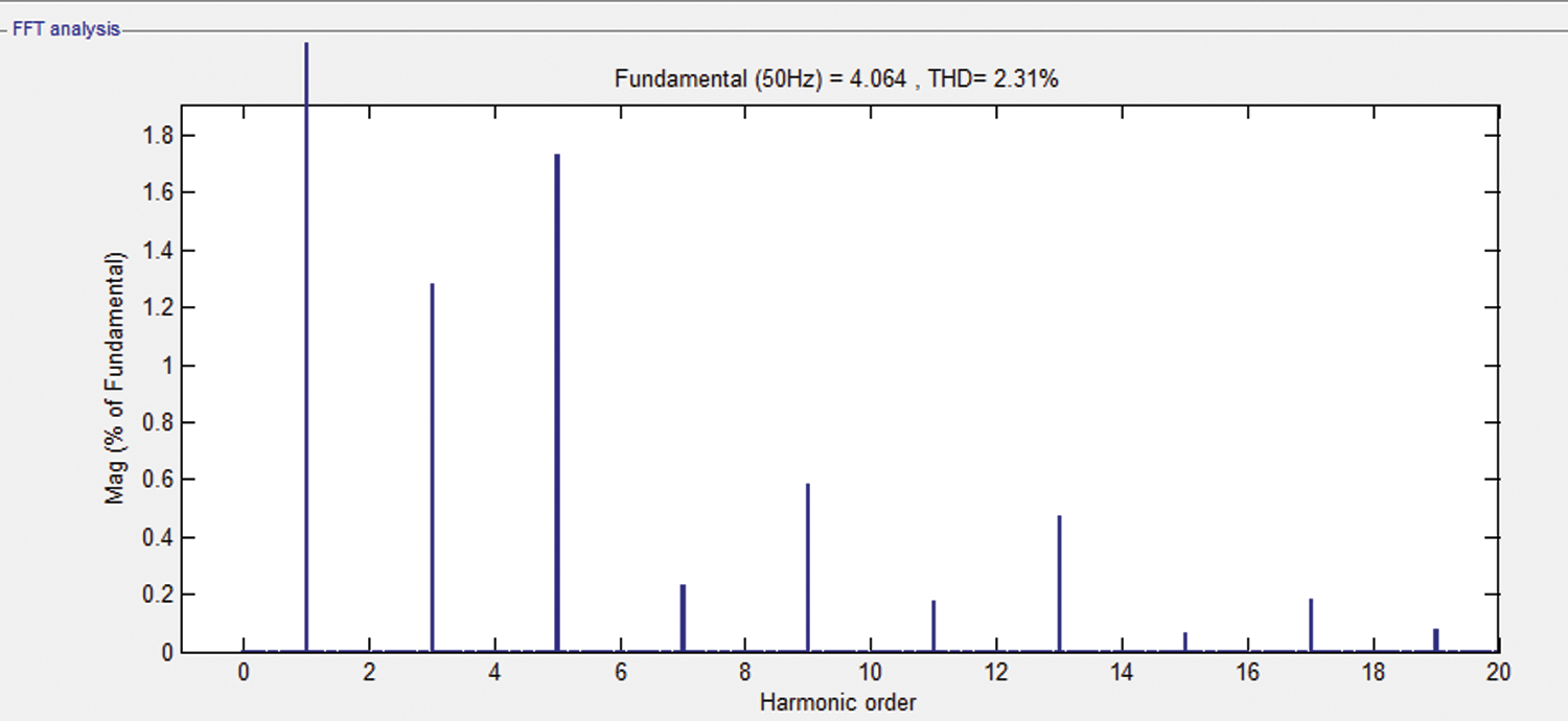
Figure 20: FFT analyses for current waveform
5 Comparative Analyses for the Different Control Method
Tab. 3 shows the performance comparisons of the proposed system with different control methods.
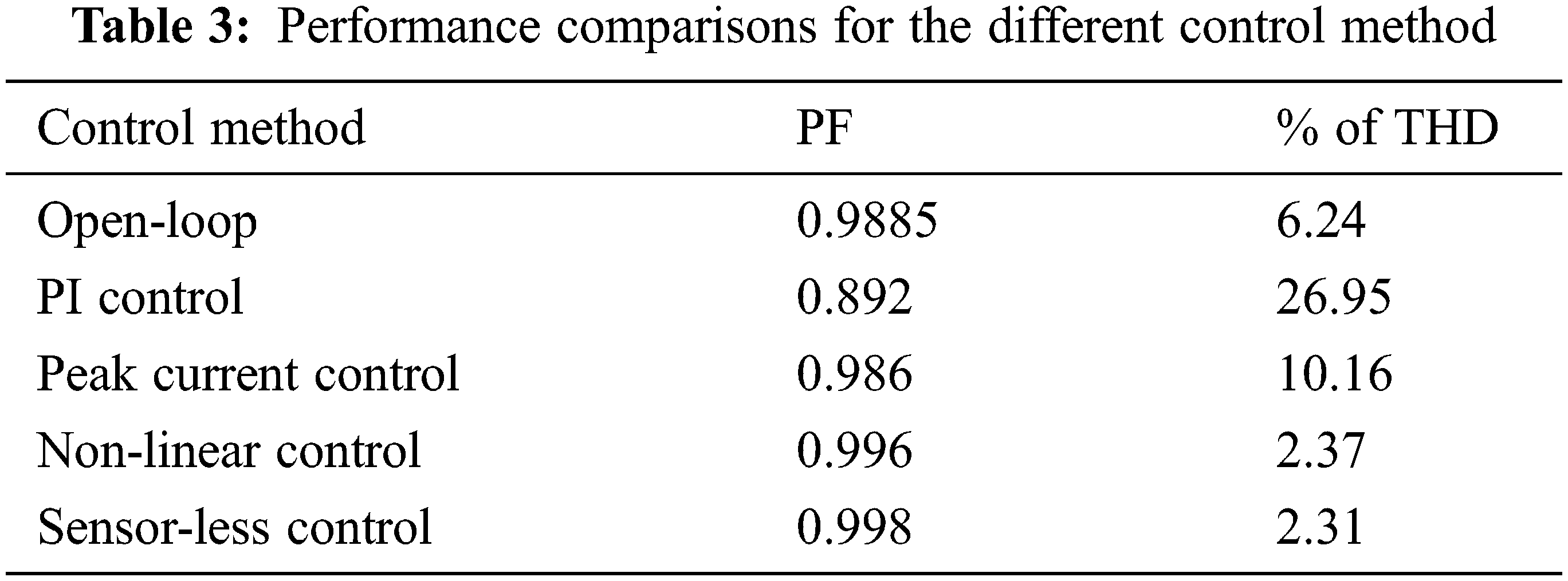
The open-loop system has a PF of 0.9885 and the proposed sensor-less closed-loop system has an input PF of 0.998. The proposed system has less THD of 2.31% than the open-loop system THD of 6.24%. The NLC method has more PF of 0.996 than the PI controller and peak current control method. Also, the NLC method has a less THD of 2.37% compared to the PI controller and peak current control method. The sensor-less control method have more PF of 0.998 than the non-linear control method that has a PF of 0.996. The sensor-less control method has less current harmonic of 2.31% compared to non-linear control method THD of 2.37%. The simulation results are coinciding with the implementation results. Thus the performance of the system is verified.
Fig. 21 shows a prototype of the proposed converter circuit diagram. DsPIC30F2010 controller is used for PWM generation with a sensor-less current control method.
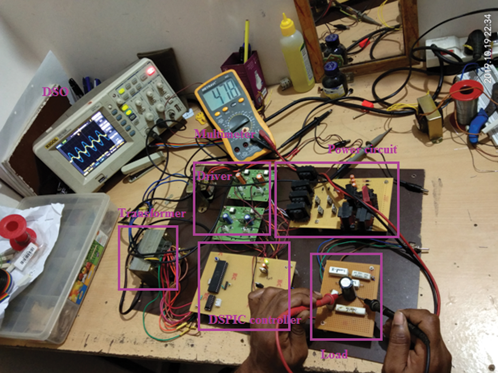
Figure 21: Experimental setup for the proposed converter
The dsPIC30F2010 is small in size and affordable controller which is excellent for applications of motor controllers. It has a strong, high-performance microchip and a high-speed core that is intended to swiftly execute the complicated calculations. It has inbuilt components such as ADC, DAC, PWM generator, and also provides fast response. The switching frequency is 10 kHz. The pulses from the PIC controller are given to MCT2E IC which is an OptoCoupler phototransistor. The term “phototransistor” implies that it is a light-based transistor (photon). It provides electrical insulation between IR LED circuit and the photo transistor circuit. The MOSFET IRF840 is used for switching the device. The IRF840 handles loads up to 8 A and 500 V on an n-canal MOSFET power. It is a high-voltage switching device that requires 10 V on the door terminal to trigger the conduction process. The IRF840 MOSFET is a three-terminal device composed of a gate, drain and source. Tab. 4 shows the list of components used for the implementation.
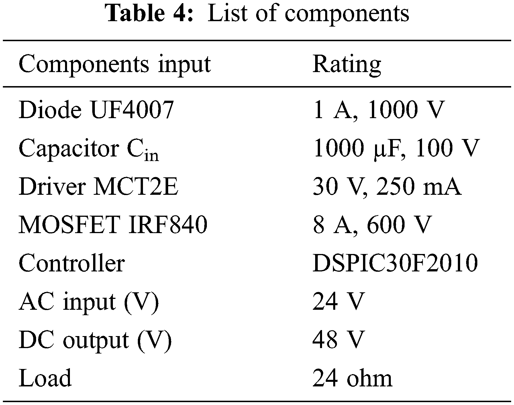
Fig. 22 shows the triggering pulse for switch S1 which is shown in blue colour and for switch S2 which is in red colour, respectively.
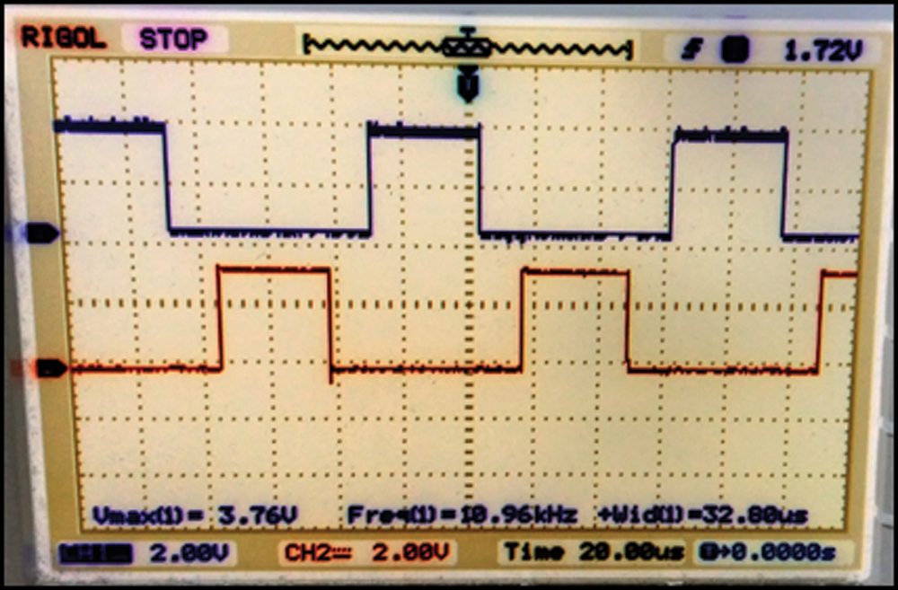
Figure 22: Gate pulse output for switch S1 and S2
Fig. 23 shows the input voltage and current waveform for the open-loop system. The input current follows the sinusoidal wave shape with distortion.
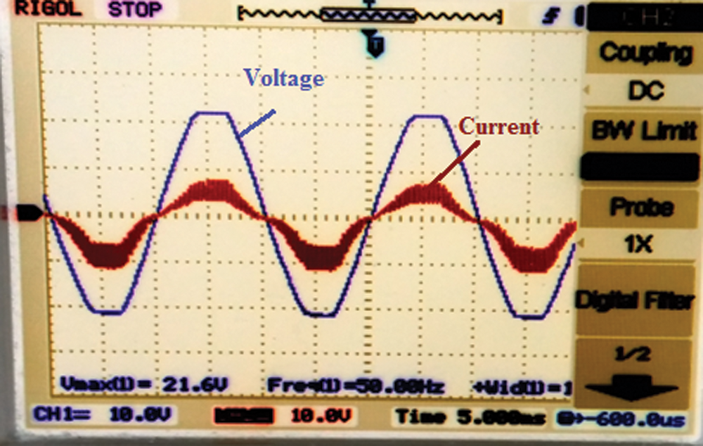
Figure 23: Input voltage and current for the open-loop system
Fig. 24 shows the input voltage and current waveform for the sensor-less current control method. The input current follows the sinusoidal shape with less distortion. The proposed converter converts AC voltage into DC voltage with boost.
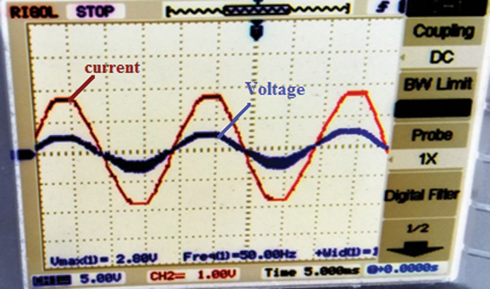
Figure 24: Input voltage and current for the closed-loop system
Fig. 25 shows the output voltage of the closed-loop system. Initially, a 25-Ω load is connected to the converter. After t = 3 min, the load value is changed from 25 to 50 Ω which changes the output voltage from 48 to 80 V suddenly. The output voltage is reduced to again 48 V immediately after a second due to the closed-loop system of the sensor-less control method. Thus the sensor-less method is used to regulate the output voltage and improves the input PF.
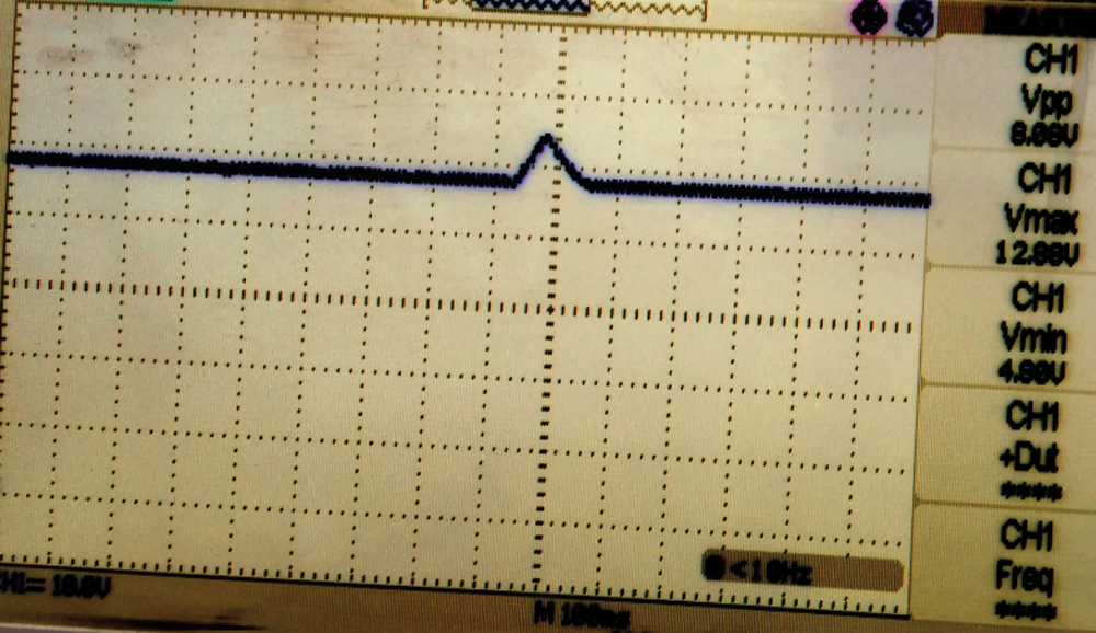
Figure 25: Output voltage for a closed-loop system
In this work, an efficient supply current wave shaping technique is presented for bridgeless interleaved SEPIC. The signal from the main switch current is contrasted with a standard NLC waveform to determine the switch duty ratio. The continuous conduction mode of interleaved bridgeless SEPIC converter is obtained by unity PF. This model can be programmed to achieve low input current THD for a broad range of loads even though it can operate discontinuously. Different control methods are discussed to increase the input PF and also minimize the current harmonics. The sensor-less control method have more PF of 0.998 than other current control methods such as open-loop (0.9885), PI control (0.892), Peak current control (0.986), and non-linear control (0.996). The sensor-less control method has less current harmonic of 2.31% than other current control methods such as open-loop (6.24%), PI control (26.95%), peak current control (10.16%), and non-linear control (2.37%). The simulation results obtained from MATLAB/SIMULINK model are coinciding with the implementation results. The sensor-less current control method brings the PF to almost unity and THD is also within the IEEE range of 5% (expand).
Funding Statement: The authors received no specific funding for this study.
Conflicts of Interest: The authors declare that they have no conflicts of interest to report regarding the present study.
1. E. F. Schubert, “History of light-emitting diodes,” in Light-Emitting Diodes, 2nd ed., New York, USA: Cambridge University Press, pp. 1–26, 2012. [Google Scholar]
2. J. Y. Tsao, “Solid-state lighting: Lamps, chips, and materials for tomorrow,” IEEE Circuits and Devices Magazine, vol. 20, no. 3, pp. 28–37, 2004. [Google Scholar]
3. S. Wang, X. Ruan, K. Yao, S. C. Tan, Y. Yang et al., “A flicker-free electrolytic capacitor-less AC-DC LED driver,” IEEE Transactions on Power Electronics, vol. 27, no. 11, pp. 4540–4548, 2011. [Google Scholar]
4. J. M. Alonso, J. Viña, D. G. Vaquero, G. Martínez and R. Osorio, “Analysis and design of the integrated double buck-boost converter as a high-power-factor driver for power-LED lamps,” IEEE Transactions on Industrial Electronics, vol. 59, no. 4, pp. 1689–1697, 2012. [Google Scholar]
5. M. He, F. Zhang, J. Xu, P. Yang and T. Yan, “High-efficiency two-switch tri-state buck-boost power factor correction converter with fast dynamic response and low-inductor current ripple,” IET Power Electronics, vol. 6, no. 8, pp. 1544–1554, 2013. [Google Scholar]
6. H. L. Cheng and C. W. Lin, “Design and implementation of a high-power-factor LED driver with zero-voltage switching-on characteristics,” IEEE Transactions on Power Electronics, vol. 29, no. 9, pp. 4949–4958, 2014. [Google Scholar]
7. Y. Chen, Z. Zhong and Y. Kang, “Design and implementation of a transformer less single-stage single-switch double-buck converter with low DC-link voltage, high step-down, and constant input power factor features,” IEEE Transactions on Power Electronics, vol. 29, no. 12, pp. 6660–6671, 2014. [Google Scholar]
8. M. Ferdowsi, “An estimative current mode controller for DC-DC converters operating in continuous conduction mode,” in 21st Annual IEEE Applied Power Electronics Conf. and Exposition, Dallas, TX, USA, pp. 19–23, 2006. [Google Scholar]
9. K. I. Hwu, H. W. Chen and Y. T. Yau, “Fully digitalized implementation of PFC rectifier in CCM without ADC,” IEEE Transactions on Power Electronics, vol. 27, no. 9, pp. 4021–4029, 2012. [Google Scholar]
10. T. Komine and M. Nakagawa, “Fundamental analysis for a visible-light communication system using LED lights,” IEEE Transactions on Consumer Electronics, vol. 50, no. 1, pp. 100–107, 2004. [Google Scholar]
11. Q. Hu and R. Zane, “Minimizing required energy storage in off-line LED drivers based on series-input converter modules,” IEEE Transactions on Power Electronics, vol. 26, no. 10, pp. 2887–2895, 2011. [Google Scholar]
12. C. S. Moo, Y. J. Chen and W. C. Yang, “An efficient driver for dimmable LED lighting,” IEEE Transactions on Power Electronics, vol. 27, no. 11, pp. 4613–4618, 2012. [Google Scholar]
13. H. J. Chiu and S. J. Cheng, “LED backlight driving system for large-scale of LCD panels,” IEEE Transactions on Industrial Electronics, vol. 54, no. 5, pp. 2751–2760, 2007. [Google Scholar]
14. X. Long, R. Liao and J. Zhou, “Development of street lighting system-based novel high-brightness LED modules,” IET Optoelectronics, vol. 3, no. 1, pp. 40–46, 2009. [Google Scholar]
15. C. W. Clark, F. Musavi and W. Eberle, “Digital DCM detection and mixed conduction mode control for boost PFC converters,” IEEE Transactions on Power Electronics, vol. 29, no. 1, pp. 347–355, 2014. [Google Scholar]
16. R. Sreemallika and R. Seyezhai, “Investigation of closed-loop current control strategies for bridgeless interleaved SEPIC converter,” Electrical and Electronics Engineering: An International Journal, vol. 3, no. 3, pp. 63–70, 2014. [Google Scholar]
 | This work is licensed under a Creative Commons Attribution 4.0 International License, which permits unrestricted use, distribution, and reproduction in any medium, provided the original work is properly cited. |