DOI:10.32604/csse.2022.022855
| Computer Systems Science & Engineering DOI:10.32604/csse.2022.022855 | |
| Article |
Capacitive Coupled Wide-Notch Stepped Impedance Narrow-Band Bandpass Filter for WiMax Application
Department of Electronics and Communication Engineering, Anand Institute of Higher Technology, Chennai, Tamil Nadu, 603103, India
*Corresponding Author: A. Kayalvizhi. Email: annamalaikayal@gmail.com
Received: 20 August 2021; Accepted: 12 October 2021
Abstract: The development of wireless communication standards necessitates optimal filter design for the selection of appropriate bands of frequencies. In this work, a compact in size pair of parallel coupled symmetric stepped impedance-based resonator is designed with supporting to the WiMAX communication standards. The coupled resonator is tuned to allow the frequency band between 3.4 GHz and 3.8 GHz, which is centered at 3.6 GHz. A parasitic effect of capacitively coupled feed structure is used for exciting the two symmetrical stepped impedance resonators. The bandwidth and selectivity of the filter are enhanced with the change of characteristic impedances and controlling the coupling gap between resonators. This design offers single narrow sharp passband selectivity as well as multiple stopband harmonic suppression arising as a result of multiple transmission zeros. The designed filter operates with a fractional bandwidth (FBW) of 11.47%. The proposed single narrowband bandpass filter provides better suppression in either side of the tuned frequency (3.6 GHz) without degrading the passband performance. Also, this novel filter offers an insertion loss of about −0.08 dB and a return loss of greater than −30 dB in passband. This approach is useful for eliminating unwanted spurious harmonics responses that enter the desired response. The suggested bandpass filter has been simulated using Advanced Design System (ADS) tool, and the measurement has been made using a network analyzer, and the results are reported.
Keywords: Single narrowband bandpass filter; fractional bandwidth; selectivity; insertion loss; return loss; transmission zeros
Advancement and technological development in wireless communication standards demand optimal design of a single band, dual-band, multi-band, and wideband bandpass filters (BPFs) which are needed for the design of Radio Frequency (RF) front end. The multi-service wireless communication systems [1], namely, Wireless Local area network IEEE 802.3 (WLAN), IEEE 802.16 Worldwide Interoperability for Microwave Access (WiMAX), and Radio-Frequency Identification (RFID) is employed with the filter design. Different techniques can be implemented in order to design a bandpass filter for Industrial, Scientific, and Medical (ISM) frequency band applications. Generally, a microwave bandpass filter consists of distributed elements of a transmission line section. These transmission line filters are designed using stepped impedances and coupled lines called coupled resonators which are widely used in industrial, medical areas, and microwave applications. A microwave two-port, reciprocal, passive, linear device attenuates unwanted signal frequencies heavily and allows only wanted frequencies.
In general, filter performance is described in terms of insertion loss, return loss, frequency selectivity, and the number of transmission zeros on either side of the passband. Bandpass filters are also designed by conversion and adjusting the lowpass prototype for meeting this requirement. The bandpass filter can be constructed using a lowpass and high pass network for the achievement of a desired band of frequencies. In conventional bandpass conversion, each lowpass prototype series inductor is transformed into a series capacitor and a series inductor. Each prototype shunt capacitor is transformed into a shunt capacitor and a shunt inductor. Therefore, the bandpass filter has two reactive elements in its proto-type design.
RF Filter is an essential part of telecommunication and radar systems. The bandpass filter is the most significant component in the front end of both the transmitter and the receiver in wireless communication. Generally, the design of the RF filter depends on a half-wavelength resonator and admittance inverters. The coupling gaps, odd mode, and even mode impedances correspond to admittance or impedance inverters. The odd-mode indicates the two signals having the same magnitude and out-of-phase characteristics. Likewise, even-mode specifies the same magnitude and in-phase signal characteristics. The use of these inverters helps the realization of BPFs separated by series or shunt inductor and capacitor (LC) resonant circuits. Then odd and even mode impedances are helpful in the calculation of the dimensions of the filters and its design transformation techniques suggested in [2]. Transmission zeros, selectivity, and fractional bandwidth play a vital role in filter design. These parameters determine the performance of filter response in various microwave structures.
There is a growing demand for single-band, dual-band, and wideband microwave devices. There are many research methodologies proposed for meeting this demand [3,4]. The design of Ultra-wideband (UWB) filters has been analyzed and expressed in [5,6]. Recently, the high selective UWB BPFs are described to enhance passband and stopband rejection in multimode resonators, stepped impedance resonators, and parallel coupled resonators [7]. Interdigital coupled lines [8] are realized in the planar microstrip structures.
The resonant frequency is obtained by a half-wavelength open-circuited transmission line resonator of uniform and non-uniform stepped impedances [9]. Here, the existence of the second resonance with n = 2 is at twice the first resonance frequency. The main drawback of the uniform impedance resonator is the occurrence of few unwanted spurious resonant modes at integer multiples of its first resonant frequency. It could be destructive to design a single-band bandpass filter. A popular technique called the realization of non-uniform stepped impedance resonators through the alternative connection of very low and high impedance of microstrip lines are helped to solve this problem. Such filters are designed conveniently and require less space. However, the usage of such filters is limited to applications where the sharp cutoff is not needed because their performance in electrical characteristics is imperfect.
The Multi-Mode Resonator (MMR) introduces five resonant modes in the passband and improved transmission zeros at the upper and the lower passband sides [10]. Here, the multiple resonance frequencies could be excited synchronously and realized to make up a wide bandwidth in the desired frequency range.
Single-band and dual-band bandpass filter designs are obtained using a multi-mode Substrate Integrated Waveguide (SIW) circular cavity resonator [11]. A miniaturized quarter-wavelength stepped impedance resonators were directly coupled for wideband achievement in [12]. A wideband bandpass filter with three coupled line cross-shaped structures is used for realizing the strong coupling in [13]. Qiang et al. [14] proposed the three cascaded transmission lines for achieving 10-dB bandwidth of 480 MHz. Further improvement on selectivity, a coupled line section is utilized. The single band-notched filter performance is achieved using the inter-digital coupling resonator structure. The asymmetric coupled line structure is used for the implementation of dual notch characteristics. A parallel coupled transmission line supports to design of many types of filters. Single-band and dual-band filter response is proposed by stepped-impedance with coupled-resonator [15].
A hexagonal shape filter is proposed with the source-load coupling for the achievement of narrow bandwidth [16]. Recently, a narrow-band balanced BPF is designed using two coupled rectangular dielectric resonators [17]. This filter is analyzed based on differential mode with low return loss (12.5 dB) in passband response and sharp roll-off in the stopband. The design of the filter is modelled by mutual inductor coupling between microstrip feed lines and two resonators. In [18], parallel-coupled lines and shorted stubs are employed to design dual-band BPF. Four transmission poles in the two passbands and the nine deep transmission zeros (TZs) in the stopband are realized. The bandwidth of the designed filter is tuned by controlling the impedance of the coupled lines and shorted stubs of moderate size. The mutual coupling between dielectric resonators (DR) is proposed on the surface of the PCB planar structure [19].
This DR is excited through microstrip feed to produce a lower cutoff, and three slots were introduced in the ground plane to produce upper cutoff frequencies. In [20–22], the spectral efficiency and optimal system parameters improved by the mutual coupling effect between the multiple input multiple output antenna terminals. The mutual coupling effect is analyzed by varying the length and the inter-distance spacing of terminals. The selection of optimal parameters is based on different channel conditions and circuit power consumption.
Usually, narrow-bandwidth filters need tightly coupled lines, and it is hard to design and fabricate in the printed circuit board. A compact size inter-digital filter can be constructed using coupled lines by folding the lines at their midpoints. The high selective single narrow passband and increased transmission zeros with multiple notch band BPF still constitute a challenge in the design area. The contributions and novelties of this article are listed as follows.
1. The proposed work shows the superior in a narrow passband at 3.6 GHz with the rejection of spurious out of band response using the distributed approach. The compact in size and simple design are implemented on a cost-effective FR4 substrate material.
2. Transmission zeros have been realized in the upper stopband without using a defective ground structure. It has achieved a better insertion loss of 0.08 dB in the passbands when it is compared with the existing methodology works, and it has also realized a better return loss greater than −30 dB in the passband.
3. The proposed work is also implemented on an equivalent schematic circuit model using the lumped element values of the Chebyshev approximation lowpass prototype. The Chebyshev approximation is modified as an elliptic bandpass structure to achieve the excellent high selectivity of both passband edges.
This paper is organized as follows. Section 1 provides an introduction to the design of the filter and the relevant literature surveys. In Section 2, coupled line resonator design is presented. The suggested BPF with a single narrowband and wide-notch characteristics are discussed in Section 3. Section 4 deals with results and discussion. Section 5 presents the conclusion and indicates the future work to be carried out.
2 Design of Coupled Line Resonator
This section describes the design of the bandpass filter using Chebyshev approximation. A wide-notched single narrow passband filter is proposed and designed to operate between 3.4 GHz and 3.8 GHz, which is specifically utilized for WiMAX applications. The planar microwave components are easier to fabricate in the printed circuit board, which has less weight, low cost, and low power consumption.
The design specifications considered are center frequency and passband edges 1.8 GHz and 1.19 GHz−2.4 GHz respectively [14]. Tab. 1 details the design specifications of the proposed Chebyshev bandpass filter. The suggested filter is of a single narrow passband for WiMAX application, and hence this design offers a narrow-bandwidth which is achieved by the appropriate selection of FBW. The proposed filter achieves a FBW of 11.47%. This shows that the filter design provides a good performance in terms of FBW as mentioned in [14] and gives an optimal FBW of less than 20% required for implementing the narrow-band design. The 50 Ω impedances are assigned at the input and output ports. The proposed filter design is operated with a fractional bandwidth of less than 20%.
where, f0 is the center operating frequency of the bandpass filter & f1, f2 denotes the edges of passband.

The design equations of a prototype lowpass filter are mentioned here. This filter design is used for the achievement of the transformation of BPF. The distributed capacitive and inductive line width and length are exploited for the formation of the relationship among the microstrip lines in the Printed Circuit Board (PCB) layout. The elementary values required for computing the filter coefficient bk of a prototype lowpass filter are denoted as β and γ and are given in Eqs. (2) and (3). The coefficient bk is a function of γ and is specified in Eq. (5). The elementary value β is required for computation of γ and its mathematical expression is given in Eq. (3). Pass band ripple LAr is used for the calculation of the elementary value β which is mentioned in Eq. (2).
The element values for a lowpass prototype were calculated with the passband ripple LAr = 0.1 dB is applied in Eqs. (2) and (3). The lowpass prototype filter coefficient values ak and bk for order n = 3 is calculated using the following Eqs. (4) and (5).
Eqs. (4) and (5) can be utilized for the determination of the proposed lumped filter element values gk for lowpass filter prototypes for 0.1 dB ripple which is referred to in Eq. (6).
Then the following design Eqs. (7)–(10) are used for the determination of the lumped inductors and capacitors element values in the series and shunt combination in the resonators. These element values could be transformed into equivalent distributed values using the transformation technique. The design values of the proposed filter can be calculated using the characteristic impedance Z0, the angular resonant frequency ω0, the lowpass prototype element values of g1, g2 and the fractional bandwidth.
Series Element
Shunt Element
The computed coefficients and the lumped element values of both series and parallel combinations in the networks are listed in Tabs. 2 and 3. They indicate the normalized Chebyshev element values for 0.1 dB ripple for the third-order filter. Inductance and Capacitance elements form a two-port network model of a bandpass filter was shown in Fig. 1b.


Figure 1: (a) Simulated layout of the proposed BPF (b) Simulated schematic circuit model of the proposed bandpass filter
Analysis of the two-port networks in high frequency ranges was made using scattering (S) parameters. Hence, in this work, the calculations were carried out in terms of S parameters. This work involves the realization of a wide-notch single narrow passband with high selectivity. The selectivity of the filter performance was finalized with the presence of transmission zeros on either side of the passband of the BPF. The proposed coupled lines impedances of even-mode Z0e and odd-mode Z0o sections were determined using the characteristic admittance Y0 and admittance inverters J. The conventional formulae are described in Eqs. (11) and (12).
The calculated impedance values from Eqs. (11) and (12) were transformed into their equivalent width, length, and space of the distributed element using the line calculator option in the ADS tool. The calculated parameter values of the proposed coupled lines impedances of even-mode and odd-mode sections are shown in Tab. 4 with Z0 = 50 Ω. These distributed microstrip line impedances are exploited in the proposed PCB layout Fig. 1a.

3 Proposed Stub Loaded Stepped Impedance with Parallel Coupled Resonator
The design of the filter is implemented based on the microstrip line and coplanar waveguide (CPW). In CPW, the filter is designed in between the top and the bottom interfaces of a substrate, and the significance of a broad coupled line section is to aim high degree of coupling. The major drawback of CPW over the strip line of microstrip circuits is lower effective dielectric constant and creation of RF loss. The designer generally prefers the microstrip-based filter design on the planar structure. Therefore, the proposed work is implemented on the basis of a microstrip line.
The microstrip bandpass filter layout is usually designed using conventional odd and even mode characteristics impedances and admittances. These odd and even mode impedances are considered in the analysis of the performance of the filter transmission. For the odd mode, the currents on two signal lines are anti-symmetric, which creates an electric wall between the two coupled lines. For the even mode, the currents on two signal lines are symmetric with the reference conductor, which creates a magnetic wall at the symmetric plane. When even and odd mode lines are not properly terminated, a portion of resonances appear along the length of a line. Therefore, the coupled lines are described by characteristics impedances that are excited at the same time to experience the different permittivity to support two quasi TEM (Transverse Electro Magnetic) modes.
Fig. 1a shows the compact size pair of symmetric stepped impedance resonators with capacitive coupled input and output feed line bandpass structure. The network used in this investigation was composed of stub loaded non-uniform stepped impedance transmission line resonators mutually coupled with other resonators. Edges of two resonators were directly coupled to each other to provide a good return loss in the passband. The layout of the proposed bandpass filter was connected with 50 Ω input and output impedance ports for better impedance match to enable the achievement of the desired filter resonance characteristics. The space between coupled lines indicates impedance inverter acting as a transmission line discontinuity for the improvement of the performance of the filter passband. The odd and even mode signals were excited through the port utilized on either side of the filter. Fig. 1b shows a schematic circuit model of bandpass filter simulated using Agilent ADS tool and a response generated with 50 Ω impedances. The calculated lumped element values in Fig. 1b are described in Tab. 3. Particularly, this schematic circuit model indicated the elliptic bandpass structure for achieving a good selectivity and desired bandwidth applications was shown in Fig. 2a. This structure consisting of two shunt capacitors is attached on either side of inductors, which provides excellent stopband performance.

Figure 2: Performance of simulated S-parameter of the proposed BPF. (a) Resonance frequency for schematic circuit model (b) Resonance frequency for EM-layout model
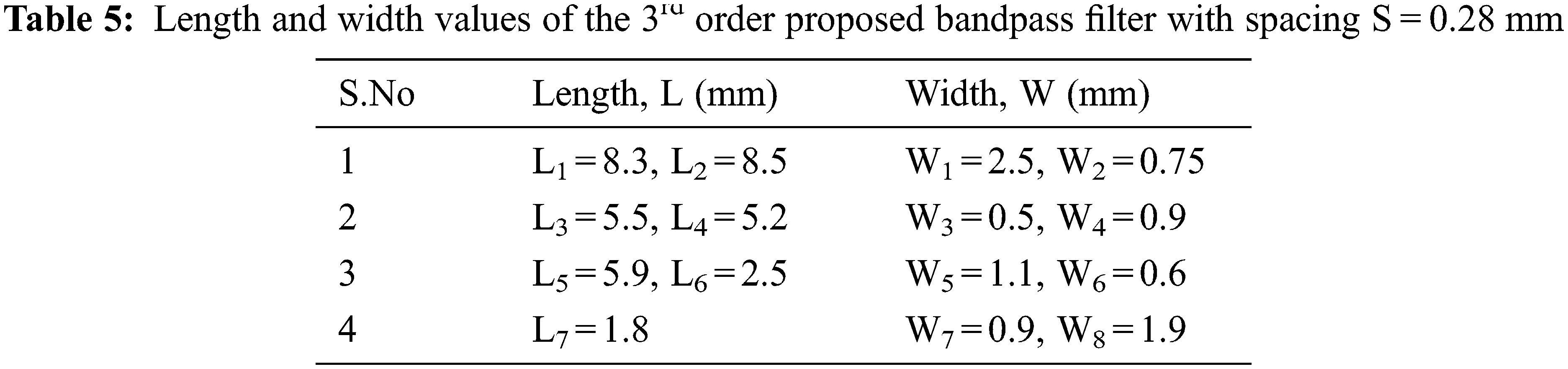
Following optimization, the proposed filter simulates a single narrow-band, and its filter design dimensions details are shown in Tab. 5. The dimensions were measured in millimeters (mm), and the spacing between the coupling was denoted as S where S = 0.288 mm. The designed filter was then fabricated and measured using a Keysight Technologies N9917A, SN: MY53101606 Network Analyzer. The proposed distributed layout design was optimized further using a momentum EM simulator for obtaining good bandpass characteristics. These impedances were used in the determination of resonant frequencies, which were implemented on a printed circuit board through the determination of the length, and width of the traces as shown in Tab. 5.
The symmetric proposed resonator was implemented using the transmission line of odd and even mode analysis method. For the odd mode, short-circuit structure was considered and analyzed. This short-circuited odd mode input admittance is expressed in Eq. (13).
where θ1 = ωL1/c indicates the electric length of open-ended transmission line. At resonance odd mode input admittance
where “c” is the velocity of light in free space. Similarly, in the even mode, analysis of the open-circuited stub structure was implemented. These resulted in the total absence of any current flow through the symmetrical structure of stub loaded resonator. Finally, the symmetrical structure was divided into two halves to enable the analysis of the even mode. The even mode admittance is given in Eq. (15).
where
Open stub was exploited for the design of the proposed bandpass filter. The electrical length of this stepped impedance stub resonator and capacitive coupled feed line structure introduce a total phase shift of 1800, which resulted in a wide-notch characteristic except for the band between 3.4 GHz and 3.8 GHz. The proposed filter was composed of two resonators that were mutually capacitive coupled to each other. Either side of open-ended transmission line edges was coupled.
Odd and even mode resonant impedances were affected on the basis of the length of the coupling lines mentioned in Eqs. (13)–(16), leading to a single narrow passband with wide-notch characteristics of the resonators. The impedances of the coupled lines are calculated by the conventional method as described in Eqs. (2)–(12). When the coupling coefficient of a particular resonant mode was zero, the resonator could not allow the field to the next one and hence, they were not excited. Capacitive coupling between source and load could be easily established using the gap between the microstrip feed line structures. Inductive coupling could be easily implemented by adding series impedances on C-shaped resonators.
Beyond 500 MHz, the filter design with discrete elements is very difficult to realize as the wavelength of the filter is compared with the physical dimensions of the filter, resulting in various losses which degrade the filter performance. Hence, the distributed element-based design approach was utilized for overcoming this difficulty. Lumped element-based filter was transformed into its equivalent distributed element using the Chebyshev approximation method and it is widely utilized as a ripple in the passband region in order to achieve a better slope in the stop-band region. Generally, passband ripples for Chebyshev approximation are considered as 0.1 dB, or 0.01 dB, or higher values. The passband ripple considered in this work is 0.1 dB.
In this section, the simulation results and analysis of the suggested bandpass filter are presented. The layout of the proposed filter was simulated using the Electro Magnetic (EM) model, and its frequency response was attained using an ADS tool. The simulation results of the proposed filter were analyzed in terms of the acceptable range of return loss better than 10 dB and minimum insertion loss of 0.2 dB. For better design, reflected power is as low as possible for the preservation of effective transmission of incident power. Likewise, the amount of output power deficit when examining input power is expressed by insertion loss S21.
The simulated return loss S11 and insertion loss S21 characteristics of the proposed schematic circuit model and EM layout model bandpass filter are depicted in Figs. 2a and 2b respectively. Narrow single-band filter performance was observed in terms of S11 and S21 parameters with high selectivity by introducing transmission zeros on either side of the passband.
Similarly, the out-of-band response and the passband response are illustrated in Figs. 3 and 4 respectively. The passband characteristics of the proposed filter provide the required confined bandwidth used in WiMAX applications. The proposed filter introduced a wide-notch on either side of the narrow passband between 3.4 GHz and 3.8 GHz respectively. The maximum insertion loss parameter S21 magnitude indicated a merely flat frequency response near 0.08-dB horizontal line over the desired passband and minimum return loss obtained in the range of 30 dB between the passband which is shown in Fig. 4. The results lead to the understanding of the proposed design offering a significant improvement in filter performance.

Figure 3: Measured and simulated S-parameters of out-of-band response of the proposed filter (a) Insertion loss (b) Return loss

Figure 4: Simulated S-parameter passband response of the proposed filter
The prototype model of the proposed BPF manufactured is shown in Fig. 5. The measurements of proposed filter S-parameter responses are compared with the simulated responses. The group delay graph is inserted in Fig. 5. The prototype design of filter was fabricated on Flame Retardant (FR4) substrate having a dielectric constant of 4.4 with a thickness of 1.6 mm. The FR4 substrate is suitable for high frequencies because the resonant frequency depends on the length of the microstrip lines and the dielectric constant of the substrates.

Figure 5: Photograph of the proposed narrow-band filter with simulated and measured S-parameters and group delay of BPF
The experimental results showed the achievement of a 3 dB fractional bandwidth of 11.47% at the center frequency of 3.6 GHz. Sub-Miniature Version A (SMA) connector on both sides of the manufactured board resulted in insertion loss of −2.21 dB instead of 0.08 dB and it is shown in Fig. 5. The difference between the measured and simulated filter responses can be obtained by the substrate dielectric loss and parasitic effects of the SMA connectors. Measurement of the proposed filter was carried out using a network analyzer. The experimental setup is shown in Fig. 6, where ports 1 and 2 of the fabricated board are connected to the two-port of the SMA connector (50 Ω) using a coaxial cable. It is observed that all the simulated results of the proposed filter are validated with measured results in terms of insertion loss, return loss, and group delay.

Figure 6: Experimental setup
Tab. 6 compares the measured parameters of the proposed work with that of the results achieved by various types of existing methodology work described in [14–16]. The proposed filter offers better performance in terms of single-band characteristics with a bandwidth of 400 MHz when examined with dual-band-based other filter designs. The unwanted noises up to the frequency range of 10 GHz in the proposed filter were eliminated. Compared with the other similar filters in the existing methodology work, it is observed that the overall performance of the proposed filter indicates an 86% of improvement in the insertion loss. Hence the proposed capacitive coupled approach-based “C” shaped filter attained the required bandwidth and a minimum loss.

In this work, a design of BPF filter has been proposed for the achievement of a single narrow-band. The proposed filter was designed for a wide-notch single narrow-band with high selectivity for WiMAX applications. The suggested filter design was compact in size and provided the enhanced out of the band rejection with a capacitive coupled feed resonator. Selectivity of the filter response was achieved through the use of controllable transmission zeros on both sides of the passband. The design parameters were tuned to enable the achievement of optimal filter performance. The designed filter, which was simulated and fabricated, was of planar type. The simulation result of the proposed filter achieved 0.08 dB insertion loss over the desired passband and a significant improvement in return loss which was less than 30 dB. This design provided a FBW of 11.47% and a bandwidth of 400 MHz between 3.4 GHz and 3.8 GHz. Based on this design concept, future work is to be carried out on the dual narrow-band design using the different Ansoft tools and the various dielectric substrates. This suggested filter can be used in communication and sensor signal processing-based applications.
Funding Statement: The authors received no specific funding for this study.
Conflicts of Interest: The authors declare that they have no conflicts of interest to report regarding the present study.
1. L. Zhu, S. Sun and W. Menzel, “Ultra-wideband (UWB) band pass filters using multiple-mode resonator,” IEEE Microwave and Wireless Components Letters, vol. 15, no. 11, pp. 796–798, 2005. [Google Scholar]
2. R. Saal and E. Ulbrich, “On the design of filters by synthesis,” IRE Transactions on Circuit Theory, vol. 5, no. 4, pp. 284–324, 1958. [Google Scholar]
3. P. Sarkar, R. Ghatak, M. Pal and D. R. Poddar, “Compact UWB band pass filter with dual notch bands using open circuited stubs,” IEEE Microwave and Wireless Components Letters, vol. 22, no. 9, pp. 453–455, 2014. [Google Scholar]
4. H. Zhu and Q. X., Chu, “Compact ultra-wideband (UWB) bandpass filter using dual-stub loaded resonators (DSLR),” IEEE Microwave and Wireless Components Letters, vol. 23, no. 10, pp. 527–529, 2013. [Google Scholar]
5. X. Y. Zhang, Y. W. Zhang and Q. Xue, “Compact band-notched UWB filter using parallel resonators with a dielectric overlay,” IEEE Microwave and Wireless Components Letters, vol. 23, no. 5, pp. 252–254, 2013. [Google Scholar]
6. M. H. Weng, C. -T. Liauh, H. -W. Wu and S. R. Vargas, “An ultra-wide band pass filter with an embedded open- circuited stub structure to improve in-band performance,” IEEE Microwave and Wireless Components Letters, vol. 19, no. 3, pp. 146–148, 2009. [Google Scholar]
7. C. H. Kim and K. Chang, “Ultra-wideband (UWB) ring resonator band-pass filter with notched band,” IEEE Microwave and Wireless Components Letters, vol. 21, no. 4, pp. 206–208, 2011. [Google Scholar]
8. P. Sing, S. Basu and Y. H. Wang, Member IEEE, “Planar ultra-wideband bandpass filter using edge coupled microstrip lines and stepped impedance open stub,” IEEE Microwave and Components Letters, vol. 17, no. 9, pp. 112–121, 2007. [Google Scholar]
9. H. Wei and Y. Yang, “A new quad-band band pass filter using asymmetric stepped impedance resonators,” IEEE Microwave and Wireless Components Letters, vol. 21, no. 4, pp. 203–205, 2014. [Google Scholar]
10. Q. X. Chu, X. H. Wu and X. K. Tian, “ “Novel UWB bandpass filter using stub-loaded multi-mode resonators,” IEEE Microwave and Wireless Components Letters, vol. 21, no. 8, pp. 403–405, 2011. [Google Scholar]
11. A. R. Azat and A. Mohan, “Single-and dual-band bandpass filters using a single perturbed SIW circular cavity,” IEEE Microwave and Wireless Components Letters, vol. 29, no. 3, pp. 602–618, 2019. [Google Scholar]
12. L. Liu, P. Zhang, M. -H. Weng, C. -Y. Tsai and R. -Y. Yang, “A miniaturized wideband bandpass filter using quarter-wavelength stepped-impedance resonators,” Electronics, vol. 8, no. 12, pp. 1540, 2019. [Google Scholar]
13. D. S. La, X. Guan, S. -M. Chen, Y. -Y. Li and J. -W. Guo, “Wideband band-pass filter design using coupled line cross-shaped resonator,” Electronics, vol. 9, no. 12, pp. 2173, 2020. [Google Scholar]
14. J. Qiang, J. Shi, Q. cao and Z. Shen, “Compact differential wideband band pass filters based on half-wavelength lines,” IEEE Microwave and Wireless Components Letters, vol. 27, no no. 10, pp. 906–908, 2017. [Google Scholar]
15. H. Zhu and A. Abbosh, “Single- and dual –band band pass filters using coupled stepped- impedance resonators with embedded coupled lines,” IEEE Microwave and Wireless Components Letters, vol. 26, no .9, pp. 675–677, 2016. [Google Scholar]
16. D. Ni, Y. Zhu and Y. Xie, “Design of hexagonal filter with source-load coupling,” Electronics Letters, vol. 23, no. 42, pp. 1560, 2006. [Google Scholar]
17. J. -X. Chen, Y. Zhan, W. Q. Ain, Z. -H. Bao and Q. Xue, “Novel narrow-band balanced bandpass filter using rectangular dielectric resonator,” IEEE Microwave and Wireless Components Letters, vol. 25, no. 5, pp. 289–291, 2015. [Google Scholar]
18. D. Li and K. -D. Xu, “Compact dual-band bandpass filter using coupled lines and shorted stubs,” Electronics Letter, vol. 56, no. 14, pp. 721–724, 2020. [Google Scholar]
19. J. Kishor, B. K. Kanaujia, S. Dwari and A. Kumar, “Bandpass filter using dielectric resonator with transmission zeros,” Microwave and Optical Technology Letters, vol. 58, no. 7, pp. 1583–1586, 2016. [Google Scholar]
20. P. Uthansakul, A. A. Khan, M. Uthansakul and P. Duangmanee, “Energy efficient design of massive MIMO based on closely spaced antennas,” Energies, vol. 11, no. 8, pp. 2029–2054, 2018. [Google Scholar]
21. A. A. Khan, P. Uthansakul and M. Uthansakul, “Energy efficient design of massive MIMO by incorporating with mutual coupling,” International Journal on Communications Antenna and Propagation, vol. 7, pp. 198–207, 2017. [Google Scholar]
22. A. A. Khan, P. Uthansakul, P. Duangmanee and M. Uthansakul, “Energy efficient design of massive MIMO by considering the effects of nonlinear amplifiers,” Energies, vol. 11, no. 5, pp. 1045–1066, 2018. [Google Scholar]
 | This work is licensed under a Creative Commons Attribution 4.0 International License, which permits unrestricted use, distribution, and reproduction in any medium, provided the original work is properly cited. |