DOI:10.32604/csse.2022.024393
| Computer Systems Science & Engineering DOI:10.32604/csse.2022.024393 | |
| Article |
An FPGA Design for Real-Time Image Denoising
Department of Electrical Engineering, Jouf University, Sakaka, Aljouf, Saudi Arabia
*Corresponding Author: Ahmed Ben Atitallah. Email: abenatitallah@ju.edu.sa
Received: 15 October 2021; Accepted: 29 November 2021
Abstract: The increasing use of images in miscellaneous applications such as medical image analysis and visual quality inspection has led to growing interest in image processing. However, images are often contaminated with noise which may corrupt any of the following image processing steps. Therefore, noise filtering is often a necessary preprocessing step for the most image processing applications. Thus, in this paper an optimized field-programmable gate array (FPGA) design is proposed to implement the adaptive vector directional distance filter (AVDDF) in hardware/software (HW/SW) codesign context for removing noise from the images in real-time. For that, the high-level synthesis (HLS) flow is used through the Xilinx Vivado HLS tool to reduce the design complexity of the HW part. The SW part is developed based on C/C++ programming language and executed on an advanced reduced instruction set computer (RISC) machines (ARM) Cortex-A53 processor. The communication between the SW and HW parts is achieved using the advanced extensible Interface stream (AXI-stream) interface to increase the data bandwidth. The experiment results on the Xilinx ZCU102 FPGA board show an improvement in processing time of the AVDDF filter by 98% for the HW/SW implementation relative to the SW implementation. This result is given for the same quality of image between the HW/SW and SW implementations in terms of the normalized color difference (NCD) and the peak signal to noise ratio (PSNR).
Keywords: AVDDF filter; image denoising; HW/SW codesign; high-level synthesis; FPGA
In the image processing application, the corruption of the image by the noise (impulsive noise, Gaussian noise, mixed Gaussian and impulsive) presents one of the most common problems. This noise is due from same limitations imperfections and can appear for example in the medical images, scanned images, during the transmission, etc. Thus, it is very important to remove the noise and repair the images before executing any subsequent task in the image processing. However, various non-linear filters are proposed in literature for images denoising such as the adaptive vector directional distance filter (AVDDF) [1], the vector directional distance filter (VDDF) [2,3], the vector directional filter (VDF) [4,5], etc. The strong point of these filters are their capability to remove the noise and repair the images without introducing a significant distortion. But unfortunately, these filters present a high computational complexity.
In this context, researchers are worked continuously to decrease the computational complexity of the non-linear filters by adopting as solution a hardware implementation on the field-programmable gate array (FPGA) circuit. In fact, in [6], the authors propose an FPGA design for the vector median filter (VMF) which is implemented and evaluated on Xilinx Spartan 3 FPGA. The experimental results show that this design can process 94 frames per second at 145 MHz. But, in [7], a hardware architecture for the VDF filter is proposed. This architecture is connected to the NIOS II processor and evaluated in hardware/software (HW/SW) codesign context. The proposed design allows to speed up the VDF filtering process. In [8], an approximated hardware design is proposed to implement the VDDF filter. This architecture provides a good balance between the filtering quality and the processing time. Nevertheless, these presented works use an estimate method of non-linear functions in order to be appropriate for low-level hardware implementation on FPGA using hardware description language (HDL) (e.g., Verilog or VHSIC hardware description language (VHDL)) which conducts to loss in the quality of the filtered images.
Over the years, the integration density in the FPGAs continues to evolve which allows to use the FPGA to implement several applications in various field such as image and video processing [9,10], IoT system [11], neural networks [12], etc. But these applications are characterized by their complexity. Hence, there is a necessity to raise the level of the design space abstraction from a traditional register-transfer level (RTL) based approach to an efficient approach to reduce the design complexity of the FPGA. Thus, the high-level synthesis (HLS) approach based on the software programming language such as C, C++, SystemC has become widely used with FPGA [13,14]. This increases the designer productivity and reduces the run-time in the design flow.
In this work, we propose an optimized HLS hardware design for the AVDDF filter in order to decrease the computational complexity and speed up the filtering process. This architecture uses a floating-point operation to implement this filter which permits to increase the accuracy of the image filtering. Also, for the performance evaluation, this filter is connected and integrated as intellectual property (IP) block with an advanced reduced instruction set computer (RISC) machines (ARM) Cortex-A53 processor in HW/SW codesign environment and evaluated on the Xilinx ZCU102 FPGA board. In fact, the HW implementation is used for performance. But the SW implementation is used for flexibility to upgrade the design [15,16].
However, in this paper, an overview of the AVDDF filter is introduced in Section 2. The HLS design flow is used to generate an optimized hardware design to implement the AVDDF filter as described in Section 3. In Section 4, the AVDDF design is integrated and evaluated in the HW/SW codesign context. In Section 5, the performance evaluation of the HW/SW implementation of the AVDDF filter is discussed. The conclusion is presented in Section 6.
The AVDDF filter [1] is designed based on the VDDF filter. It provides the benefits of the treatment by the direction and the magnitude. Furthermore, it improves the filtering process by using a threshold as reported in Fig. 1. Indeed, through this threshold, the AVDDF filter can determine whether the pixel contains noise or not.
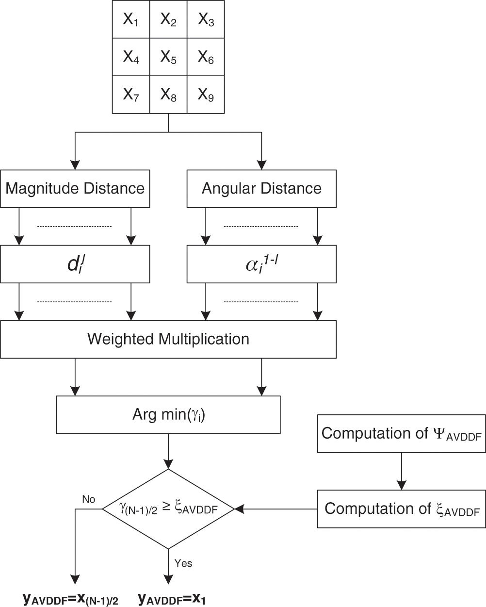
Figure 1: AVDDF algorithm
We consider by
where
The output
In Eq. (3), the
where
However, when
Recently, the HLS flow is used with FPGA to help engineers to explore the design space in fraction of time from a given behavioural description based on a high-level programming language (e.g., SystemC, C/C++, etc). For that, the HLS is emerged as an efficient and powerful tool to increase the productivity of design and decrease the design cycle time. In this context, different HLS tools are elaborated like Xilinx Vivado HLS tool which proposes several directives to generate an optimized hardware architecture for any algorithms. In fact, the arrays can be implemented as registers or memories through the RESOURCE directive. Besides, the implementation of the arithmetic operation can be optimized using ALLOCATION directive. Furthermore, the loops can be pipelined or not unrolled or fully/partially unrolled through the PIPELINE and UNROLL directives to reach a higher throughput for the loop iterations.
Nevertheless, Fig. 2 presents the block diagram of the hardware architecture generated for AVDDF filter using Xilinx Vivado HLS 18.1 tool from a specific C/C++ code. In fact, some directives (such as PARTITION, PIPLINE, RESOURCE) are added incrementally to the AVDDF C/C++ code to generate various AVDDF hardware designs. Indeed, our goal is to select an optimized design that gives a compromise between hardware cost and processing time. By the way, Tab. 1 shows the hardware resources needed for the different AVDDF designs under the Zynq XCZU9EG FPGA in terms of Look-up-table (LUTs), Flip-Flops (FFs), BRAM blocks and DSP blocks. But Fig. 3 illustrates the number of the clock cycles for HLS AVDDF generated design.
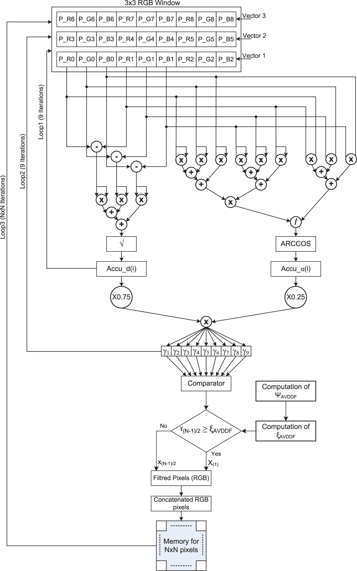
Figure 2: Proposed AVDDF filter block diagram
From Tab. 1, we can see that the FPGA resources required for the design 1 which presents the hardware architecture without any optimization is equal to 12% of LUTs, 3% of FFs, 10% of BRAMs and 18% of DSPs. But design 1 needs 2041947658 clock cycles to filter all pixels in the image as reported in Fig. 3. It is clear that the number of clock cycles is very high and must be reduced. For that, we suggest to generate design 2 by applying the PARTITION directive which allows to split the filtering window (Fig. 2) to small blocks and promote parallel access to data. According to Fig. 3 and Tab. 1, design 2 permits to decrease the number of clock cycles by 0.7% but with an increase by 20% of LUTs and 28% of FFs compared to design 1. From these results, we notice that the number of clock cycles is still high. For that, more directives should be added to decrease the number of clock cycles.
From Fig. 2, we can constate that the AVDDF filter contains three Loops. Loop1 needs 9 iterations. Loop2 needs 81 iterations. Loop3 needs 5308416 iterations. Thus, to decrease the number of clock cycles needed for the Loop3, the design 3 is generated by applying the PIPLINE directive. As shown in Fig. 3, the number of clock cycles is decreased by 99% for design 3 compared to design 2 but with an overflow in the FPGA space by 59% in term of LUTs (Tab. 1). Consequently, the RESOURCE directive is used. This allows to reduce the hardware cost by 67% in term of LUTs for design 4 relative to design 3 as illustrated in Tab. 1 with a raise by 81% in number of clock cycles (Fig. 3). When, we compare design 4 and design 2, we can notice that design 4 provides a decrease in number of clock cycles by 99% and uses more LUTs by 69% relative to design 2.
Subsequently, the design 4 is selected to implement and evaluate the AVDDF filter in HW/SW codesign context. In fact, this design allows a compromise between hardware cost and processing time.
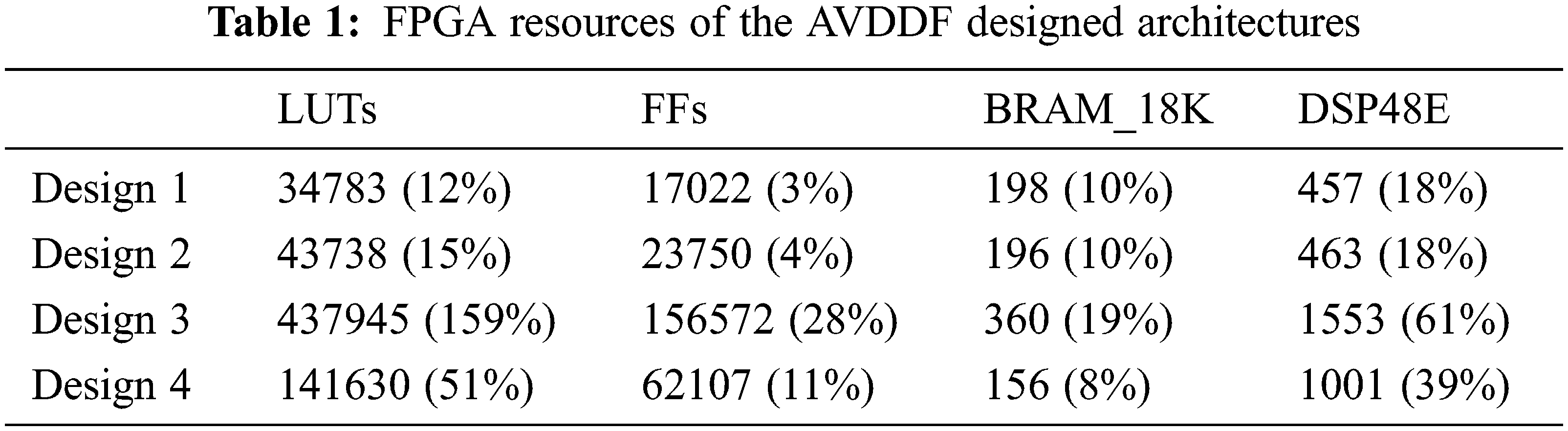
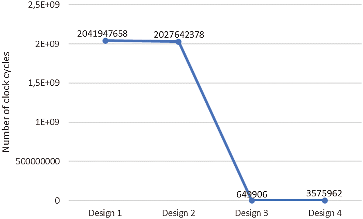
Figure 3: Number of clock cycles of the AVDDF architectures
4 HW/SW Implementation of the AVDDF Filter
The ZCU102 FPGA board [17] is selected to implement the AVDDF filter in HW/SW codesign context. The heart of this board is the Zynq XCZU9EG FPGA. Besides, this board contains many input/output devices such as 4 GB 64-bit DDR4 memory, 64 MB flash memory and SD card support which permits to designers to develop several designs for various applications such as automotive, video, industrial and communications.
The Zynq XCZU9EG FPGA contains the Programmable Logic (PL) and Processing System (PS) parts. The PS part is based on the ARM Cortex-A53 hardcore processor operating at 1.2 GHz. The ARM Cortex-A53 is a Harvard 64-bit processor and designed based on Armv8-A architecture. In this processor, the size of the L1 cache memory for data and instruction is equal to 32 KB. But the size of the L2 cache is 1 MB. On the other hand, the PL part contains 274 k of LUTs, 548 k of FFs, 32.1 Mb of BRAM memory and 2520 DSPs blocks. The Zynq XCZU9EG FPGA is completed by industry standard advanced extensible interface (AXI) protocol interface which defined by ARM. The AXI interface provides a high bandwidth, low latency connection between the PS and PL parts. Nevertheless, there are two main AXI4-interfaces: AXI4-Stream and AXI4-Lite [9]. Indeed, the AXI4-Stream provides a high-speed streaming data by using point-to-point streaming data without indicating any addresses. But the AXI4-Lite is a traditional low throughput memory communication which is used for status and control registers. However, with Zynq FPGA, Xilinx proposes an efficient HW/SW design flow through the Xilinx Vivado design 18.1 tool as presented in Fig. 4. This flow allows to accelerate design time and time-to-market (TTM). In fact, according to Fig. 4, the Vivado HLS tool is used through a SW specification such as C/C++ programming language and particular directives to develop an optimized RTL architecture. Then, when the HLS synthesis is completed, the compressed file (.ZIP) including all HDL files is generated and exported to the Xilinx Vivado tool which is used to implement a multiple accelerators blocks connected to the embedded processor across an AXI interface. This interface is created through the Vivado HLS tool. After that, the Xilinx Vivado tool synthesizes, implements and generates the Bitstream file (.bit) of the HW/SW design. Thereby, the HW/SW architecture of the AVDDF filter is designed based on this flow as depicted in Fig. 5.
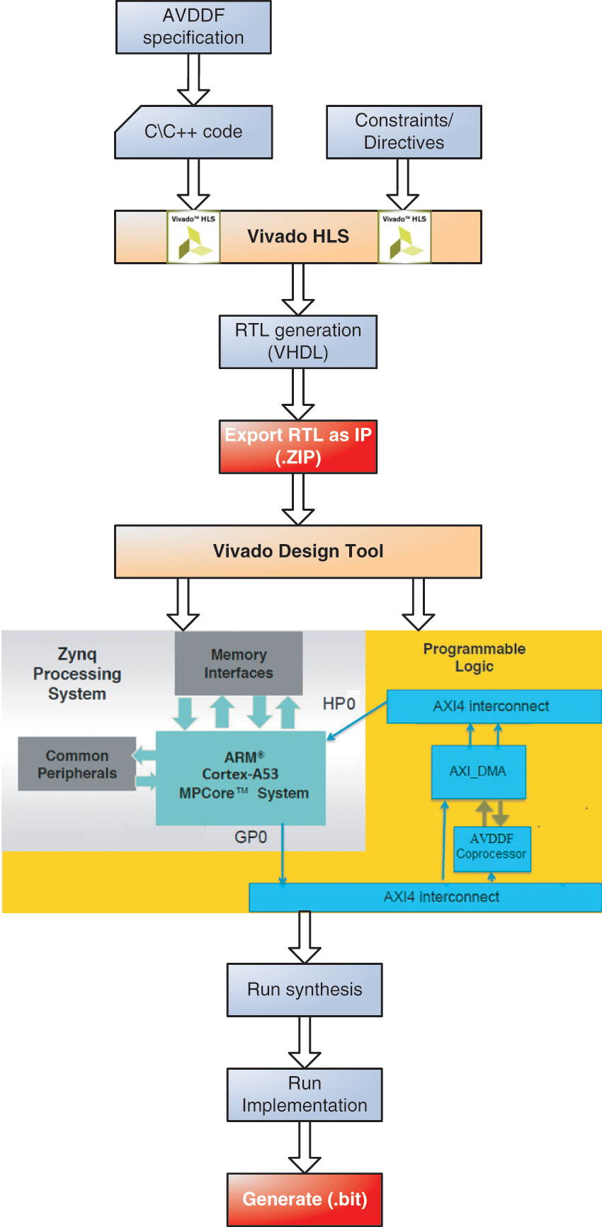
Figure 4: Xilinx Vivado design flow
According to Fig. 5, the AXI4-stream interface is used through the Direct Memory Access (DMA) to interconnect and transfer data between the PS and PL (AVDDF coprocessor) parts. In fact, the DMA provides a high throughput for data transfer. However, our architecture receives three image lines from DDR memory through three DMAs (DMA1, DMA2 and DMA3). Each 24-bit RGB pixel received by the AVDDF coprocessor is stored in internal memory. Once the 3 × 3 filtering window is constructed, the AVDDF filter starts to find the pixel which it has the minimum magnitude/angular distance. Then, the 24-bit RGB filtered pixel is concatenated and stored in the internal image memory. For the following filtering window, only three 24-bit RGB pixels are added with one RGB pixel for each line as shown in Fig. 6. In the end, when all RGB pixels in the noisy image are filtered, the DMA1 is used to transfer all RGB pixels of the filtered image from the internal memory to the DDR memory. After that, the ARM Cortex-A53 reads the data from DDR and reconstructs the image.
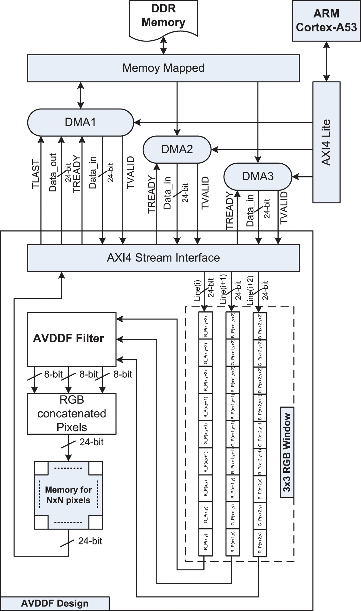
Figure 5: HW/SW architecture for AVDDF filter
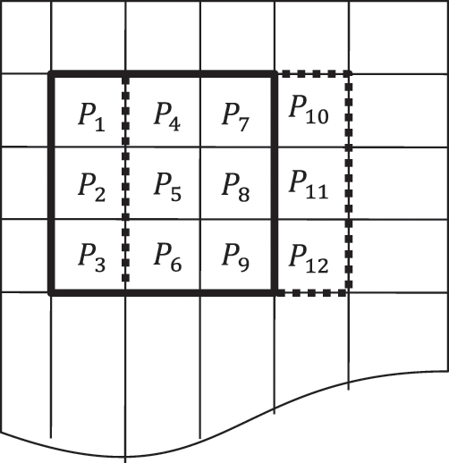
Figure 6: Construction of the 3 × 3 filtering window
The HW/SW AVDDF design is evaluated on the ZCU102 board in terms of processing time, quality of the filtered images and hardware cost. For that, various standard test images (e.g., Lena, Flower, Sailboat, Peppers and Monalisa) are uploaded in the SD card of the ZCU102 board. The size of these standard images is 256 × 256 pixels. Besides, these images are corrupted by “salt and pepper” impulsive noise. Besides, the ARM Cortex-A53 timer is used to measure the processing time. Further, the objective measurement [18] are used to determine the quality of the filtered images by using the normalized color difference (NCD) [19] and the peak signal to noise ratio (PSNR) which are defined by eqs. (6) and (7), respectively.
where
where (i,j) is the indices of a sample in the image, M and N characterizes the image size, k characterize the color channel,
Moreover, our design is synthesized using Xilinx Vivado design 18.1 tool to determine the hardware cost. Fig. 7 reports the hardware cost in terms of LUTs, FFs, BRAM and DSP. From, this figure, we can notice that our design requires 46% of LUTs, 10% of FFs, 8% of BRAM and 35% of DSP blocks which keep more FPGA resources to add more hardware blocks.
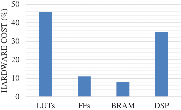
Figure 7: Hardware cost of the HW/SW AVDDF design on the XCZU9EG FPGA
The SW part is developed using C/C++ programming language. In our code the transfer of pixels between the DDR memory and HW part is controlled by three DMAs through the instructions presented in Fig. 8. Indeed, the DMA1 is addressed by the address of the 1st line of image, DMA2 by 2sd line and DMA3 by 3rd line. The DMA1 is used also to transfer the filtered image from HW part to DDR memory. So, DMA1 is configured in read/write mode. Besides, the “ff.h” library is added to our code in order to manage the reading and writing of images from/to SD card. However, our C/C++ code is developed and compiled through the Xilinx Software Development Tool Kit (SDK) based on the hardware specification as presented in Fig. 9. Thus, in our case, the executable file (.elf) is generated through the SDK to be performed by the ARM Cortex-A53 processor on standalone application mode.
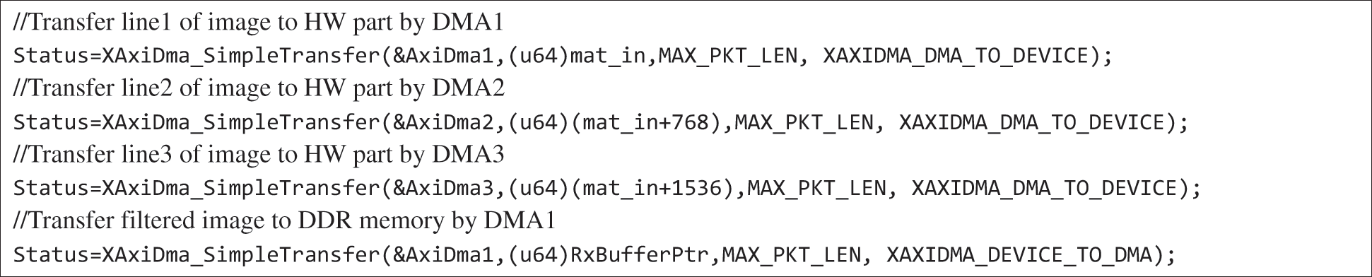
Figure 8: Transfer data between HW part and DDR memory by three DMAs
According to the Fig. 9, once the executable file (.elf) is generated, it is loaded with the Bitstream file (.bit) on the FPGA board. Our program is performed by the Cortex-A53 processor to read the noisy images from the SD card, process them by the AVDDF filter and store the filtered images in the SD card. Then, the computer is used to read the filtered images from the SD card and evaluate the image quality.
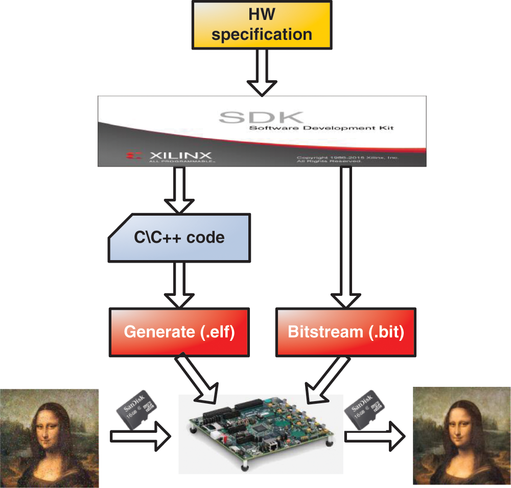
Figure 9: HW/SW codesign evaluation process
Tabs. 2 and 3 report the comparison of the processing time and the quality of the filtered images, respectively, for the SW and HW/SW implementations of the AVDDF filter.
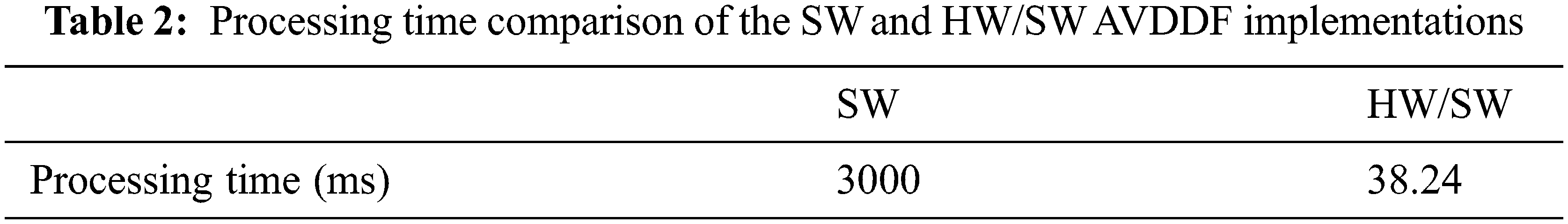
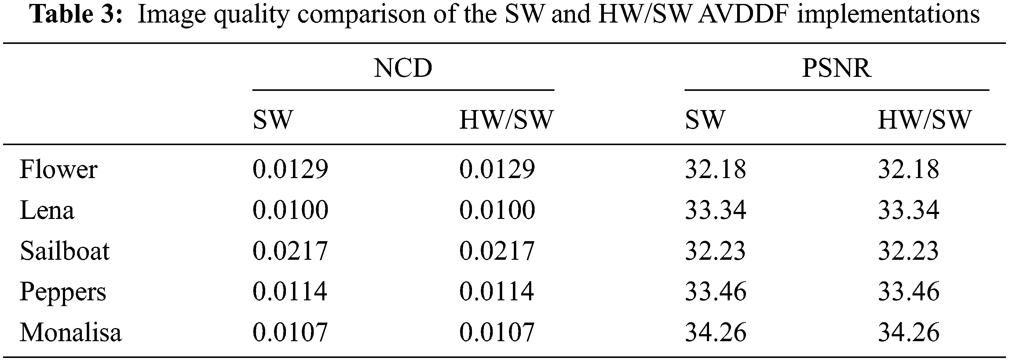
In fact, from Tab. 2, we can notice that the HW/SW AVDDF design is 79 times faster than the SW implementation which permits an improvement in processing time by 98% for the HW/SW AVDDF implementation relative to SW implementation of the AVDDF filter. This result is given for the same the quality of the filtered images in terms of NCD and PSNR between these two implementations as shown in Tab. 3. As well, the quality of the filtered images, it is confirmed by the subjective measurement as presented by Fig. 10. This quality is confirmed also for medical image. Indeed, we cannot notice any difference between the images filtered by SW and HW/SW implementations. Therefore, we can conclude that the HW/SW AVDDF design provides better results relative to the SW implementation despite of the HW part is implemented in floating-point through the HLS flow. From Tab. 4, we can conclude that our design is more performant than [7,8,20] in spite of that the AVDDF is more complex than the VDF, DDF and VDDF filters.
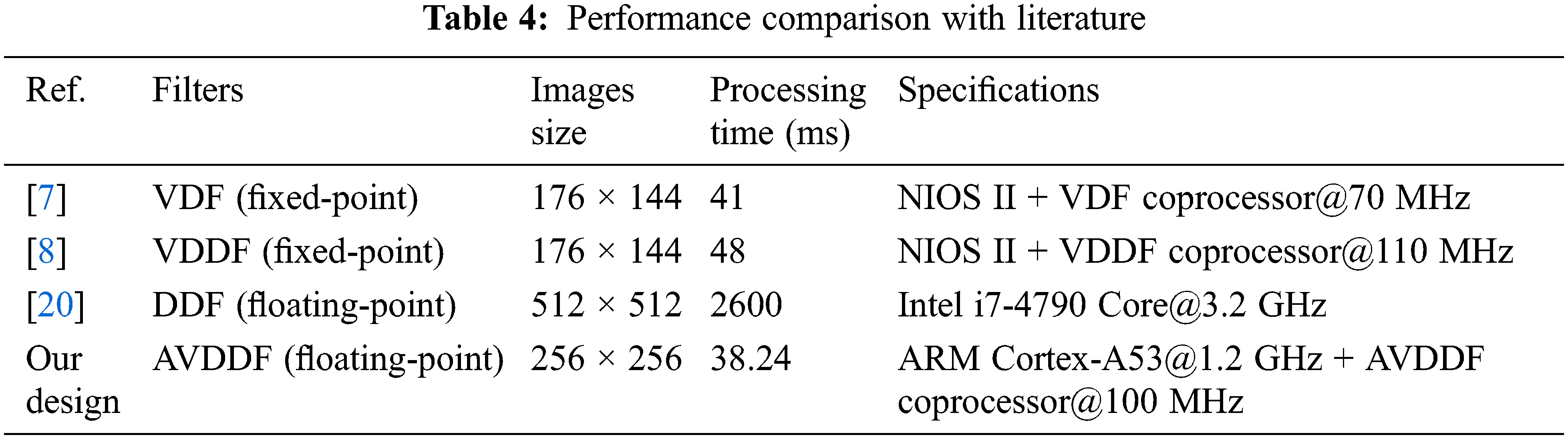
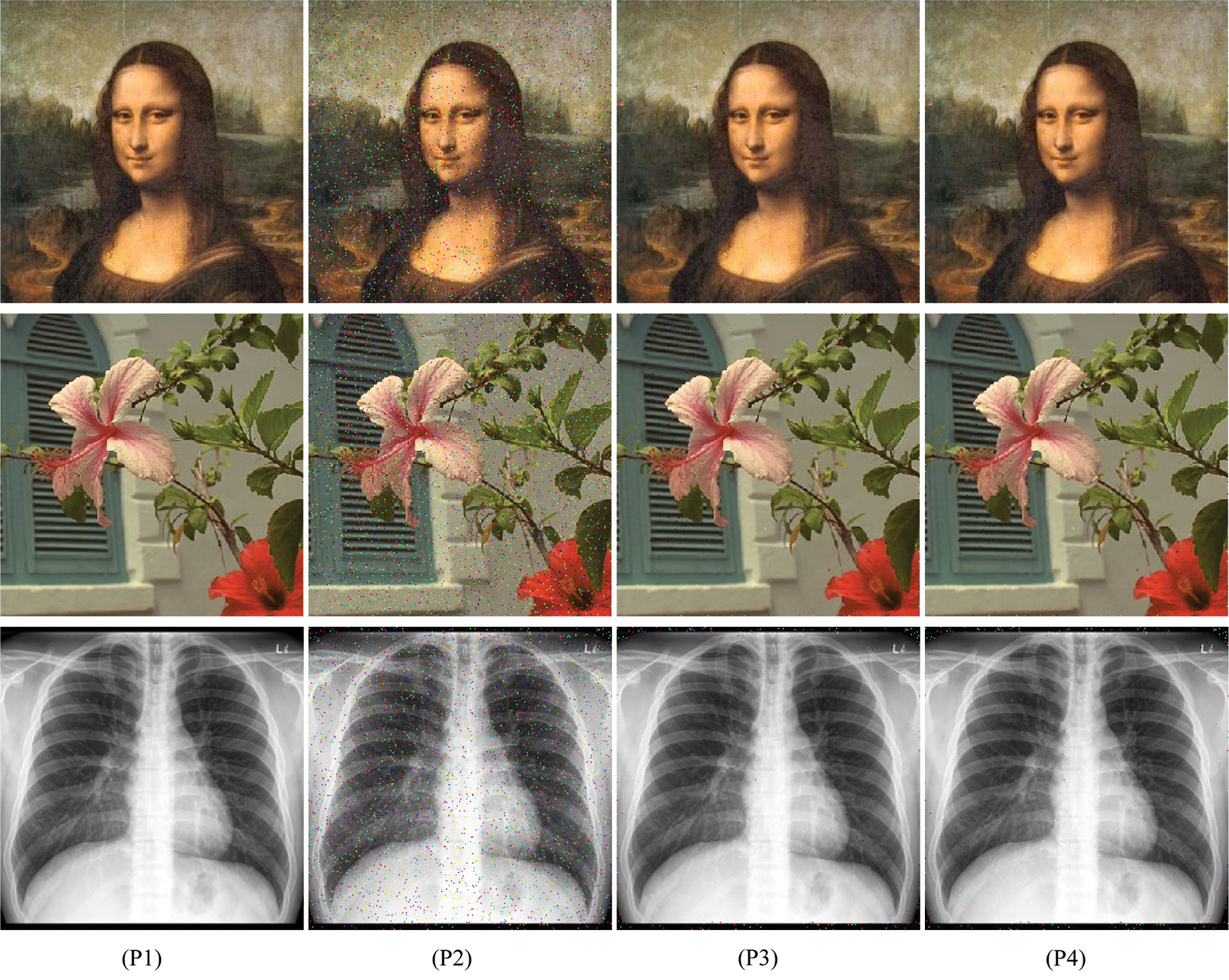
Figure 10: (P1) Original images, (P2) contaminated images with impulsive noise (3%), filtered images with (P3) SW and (P4) HW/SW AVDDF implementations
In this work, an efficient HW/SW AVDDF design is proposed to remove noise from corrupted images. However, an optimized HW architecture in terms of hardware cost and number of clock cycles is designed using the HLS flow through the Xilinx HLS Vivado tool. This architecture is designed by adding PARTITION, PIPLINE and RESOURCE directives to the floating-point AVDDF C/C++ code. The AXI-stream protocol interface is used through the DMAs to accelerate the data transfer between the AVDDF coprocessor and PS part. The HW/SW AVDDF design is evaluated on ZCU102 FPGA board. The experiment results report that the HW/SW implementation permits to speed up the processing time by 78 times with the same quality of the filtered images compared to the SW implementation.
Funding Statement: This work was funded by the Deanship of Scientific Research at Jouf University (Kingdom of Saudi Arabia) under Grant No. DSR-2021-02-03106.
Conflicts of Interest: The author declares that they have no conflicts of interest to report regarding the present study.
1. I. Abid, A. Boudabous and A. Ben Atitallah, “Reduction of impulsive noise in colour image using an adaptive vector distance directional filter,” in Proc. of the IEEE Conf. on Advanced Technologies for Signal and Image Processing, Monastir, Tunisia, 2016. [Google Scholar]
2. L. Khriji, “Vector directional distance rational hybrid filters for color image restoration,” Journal of Engineering Research, vol. 2, no. 1, pp. 1–11, 2005. [Google Scholar]
3. D. G. Karakos and P. E. Trahanias, “Combining vector median and vector directional filters: The directional-distance filters,” in Proc. of the IEEE Conf. on Image Processing, Washington, DC, USA, 1995. [Google Scholar]
4. P. E. Trahanias and A. N. Venetsanopoulos, “Vector directional filters – a new class of multichannel image processing filters,” IEEE Transactions on Image Processing, vol. 2, no. 4, pp. 528–534, 1993. [Google Scholar]
5. R. Lukac, B. Smolka, K. N. Plataniotis and A. N. Venetsanopoulos, “Selection weighted vector directional filters,” Computer Vision and Image Understanding, vol. 94, no. 1, pp. 140–167, 2004. [Google Scholar]
6. Ozgur Tasdizen and Ilker Hamzaoglu, “Computation reduction techniques for vector median filtering and their hardware implementation,” in Proc. of the IEEE Conf. on Digital System Design: Architectures, Methods and Tools, Lille, France, 2010. [Google Scholar]
7. A. Ben Atitallah, A. Boudabous, L. Khriji and N. Masmoudi, “Reconfigurable architecture of VDF filter for multidimensional data,” International Journal of Circuit Theory and Applications, vol. 41, no. 10, pp. 1047–1058, 2012. [Google Scholar]
8. A. Boudabous, A. Ben Atitallah, L. Khriji, N. Masmoudi and P. Kadionik, “Efficient FPGA implementation of vector directional distance filters based on HW/SW environment validation,” International Journal of Electronics and Communications, vol. 65, no. 3, pp. 250–257, 2010. [Google Scholar]
9. M. Kammoun, A. Ben Atitallah, R. Ben Atitallah and N. Masmoudi, “Design exploration of efficient implementation on SoC heterogeneous platform: HEVC intra prediction application,” International Journal of Circuit Theory and Applications, vol. 45, no. 12, pp. 2243–2259, 2017. [Google Scholar]
10. A. Ben Atitallah, H. Loukil, P. Kadionik and N. Masmoudi, “Advanced design of TQ/IQT component for H.264/AVC based on SoPC validation,” WSEAS Transactions on Circuits and Systems, vol. 11, no. 7, pp. 211–223, 2012. [Google Scholar]
11. Y. Chen, J. He, X. Zhang, C. Hao and D. Chen, “Cloud-DNN: An open framework for mapping DNN models to cloud FPGAs,” in Proc. of the ACM/SIGDA Int. Sym. on Field-Programmable Gate Arrays, New York, NY, USA, pp. 73–82, 2019. [Google Scholar]
12. X. Zhang, A. Ramachandran, C. Zhuge, D. He, W. Zuo et al., “Machine learning on FPGAs to face the IoT revolution,” in Proc. of the Conf. on Computer-Aided Design, Irvine, CA, USA, pp. 894–901, 2017. [Google Scholar]
13. A. Ben Atitallah, M. Kammoun, K. M. A. Ali and R. Ben Atitallah, “An FPGA comparative study of high-level and low-level combined designs for HEVC intra, inverse quantization, and IDCT/IDST 2D modules,” International Journal of Circuit Theory and Applications, vol. 48, no. 8, pp. 1274–1290, 2020. [Google Scholar]
14. M. Kammoun, A. Ben Atitallah, K. M. Ali and R. Ben Atitallah, “Case study of an HEVC decoder application using high-level synthesis: Intra prediction, dequantization, and inverse transform blocks,” Journal of Electronic Imaging, vol. 28, no. 3, pp. 1, 2019. [Google Scholar]
15. A. Ben Atitallah, M. Kammoun and R. Ben Atitallah, “An optimized FPGA design of inverse quantization and transform for HEVC decoding blocks and validation in an SW/HW environment,” Turkish Journal of Electrical Engineering & Computer Sciences, vol. 28, no. 3, pp. 1656–1672, 2020. [Google Scholar]
16. A. Boudabous, M. A. Ben Atitallah, R. Kachouri and A. Ben Atitallah, “HW/SW design and FPGA implementation of the GCM for an efficient text extraction from complex images,” International Journal of Scientific & Technology Research, vol. 9, no. 3, pp. 6572–6581, 2020. [Google Scholar]
17. Xilinx, “Xilinx Zynq UltraScale+ MPSoC ZCU102 Evaluation Kit,” 2021. [Online]. Available: https://www.xilinx.com/products/boards-and-kits/ek-u1-zcu102-g.html#hardware. [Google Scholar]
18. R. Lukac, B. Smolka, K. N. Plataniotis and A. N. Venetsanopoulos, “Selection weighted vector directional filters,” Computer Vision Image Understanding, vol. 94, no. 1, pp. 140–167, 2004. [Google Scholar]
19. K. N. Plataniotis and A. N. Venetsanopoulos, Color image processing and applications. Berlin: Springer, 2000. [Google Scholar]
20. L. Jin, Z. Zhu, E. Song and X. Xu, “An effective vector filter for impulse noise reduction based on adaptive quaternion color distance mechanism,” Signal Processing, vol. 155, no. 12, pp. 334–345, 2019. [Google Scholar]
 | This work is licensed under a Creative Commons Attribution 4.0 International License, which permits unrestricted use, distribution, and reproduction in any medium, provided the original work is properly cited. |