DOI:10.32604/csse.2023.025575
| Computer Systems Science & Engineering DOI:10.32604/csse.2023.025575 | |
| Article |
Computerised Gate Firing Control for 17-Level MLI using Staircase PWM
1Department of Electronics and Communications Engineering, Kalaignar Karunanidhi Institute of Technology, Coimbatore, Tamilnadu, 641402, India
2Department of Electrical and Electronics Engineering, Anna University, Regional Centre Coimbatore, Tamilnadu, 641046, India
*Corresponding Author: M. Geetha. Email: geethampapers@gmail.com
Received: 29 November 2021; Accepted: 11 January 2022
Abstract: A basic 7-level MLI topology is developed and the same is extended to the 9-level then further increased to 17-levels. The developed structure minimizes the component’s count and size to draw out the system economy. Despite the various advantages of MLIs, efficiency and reliability play a major role since the usage of components is higher for getting a low Total Harmonics Distortion (THD) value. This becomes a major challenge incorporated in boosting the efficiency without affecting the THD value. Various parametric observations are done and realized for the designed 9-level and 17-level MLI, being the Total Standing Voltage (TSV), efficiency, cost function per level count, and power loss. The respective parameters are compared with several existing and modern circuits and found to be effective in their performance. A novel single-phase 17-level asymmetrical Multi-Level Inverter (MLI) topology is developed to reduce the number of overall components. The developed topology generates 17-levels by using unequal DC sources. The developed MLI is proved under various tests conducted experimentally for the various loads like resistive, inductive, and combinational loads. A detailed comparison is done on several factors and represented graphically represented. Further, the proposed design provides a less TSV value is 6 Vdc, efficiency is 94.21% and cost factor per level CF/L value for both values of α is 2.01 and 2.05 and devices count with a low THD value 41.4% with respectively.
Keywords: Inverters; 9-level and 17-level MLI; switches count; load current; voltages; round-robin staircase PWM
The multilevel inverter has grown in popularity in recent years due to several advantages, such as less harmonic content, fewer switching losses, and lower electromagnetic interferences [1]. Most commonly the demand for the MLIs is gradually increasing with the power conversion process i.e., from Direct Current (DC) - (AC) Alternating Current, DC-DC & AC-DC, and along with the applications like AC motor drives, active capacitive filters, electric vehicles, uninterrupted power supplies, etc. [2]. These types of MLIs provide a step voltage wave at the output and employ several DC sources with a power semiconductor interface, consisting of several switches [3]. Even though the traditional MLI topologies like Neutral point clamped (NPC), Flying capacitors (FC), and Cascaded H-bridge (CHB) are utilized at maximum in various industrial automated applications, still there are some disadvantages such as high device count in CHBs and unequal voltages in FC and NPC MLI topologies. The reliability of the NPC type of MLI has diminished due to the usage of diodes in the system [4].
The most demanding issues in operating the MLI are commonly the devices and switches count, balancing the capacitive voltages, TSV, employing the chance of incorporating asymmetric sources in the structure [5]. In the modern advanced technology, several MLI topologies are proposed concerning the combinations of several capacitors and DC sources concerning the various switching states. In [6], an advanced H-bridge MLI with various DC sources is presented. A 7-level MLI topology proposed in [7], utilizes 9 switches and 3 DC sources and tends to combine all DC levels at its voltage output. In [8], an MLI is introduced with eight switches making up the 7-level output and 3 DC sources having a cascaded structure that utilizes a half-bridge circuitry. Several modulation techniques are used in the MLI topologies, specifically the phase opposition and disposition technique is used in [9]. Novel 7-level MLI structure is proposed in [10] aims to reduce overall components like switches, sources, elements in the circuit and the A PI controller controls the current, which is not effective. The major disadvantage is that the modulation technique's complexity becomes high while the level count is raised, [11,12]. Further, the levels of MLI get increased to have more advantages related to reliability and efficiency. The topology presented in [13] is a 9-level MLI, consists of twelve switches, and the various units are cascaded in [14]. The author in [15] presented a 9-level MLI consisting of two capacitors and one DC source. An asymmetrical 17-level MLI topology is designed from the basic 7-level and 9-level MLI structures. Hence, both 9 and 17-level MLIs are accomplished in detail along their outcomes are observed to be advantageous when correlated with various conventional and modern topologies. The major advantages of the proposed structure involve the rapid increase in its output levels with lesser devices count. The TSV shows the peak voltage which is blocking at the switches and is obtained. However, the cost-function and cost-function per level count values are calculated based on the TSV value. Efficiency calculations along with power losses are calculated in detail, these extracted outcomes are compared in detail along with the several modern topologies. Experimental efficiency is calculated and compared with the simulation results. A developed MLI is cost-effective since it uses a low TSV value and has a high-efficiency value. Comparison is made between the respective power losses and efficiencies for all loads. The THD value is following IEEE standards. The developed topology is applied to applications like active filters, UPS, renewable energy sources, and FACTS. In this paper, a 17-level switched diode MLI is precisely tested under numerous loads including resistive, inductive, and combinational loads including both resistive and inductive loads. The challenges and practical recommendations for developing an efficient system were highlighted. In order to motivate and guide society to focus on developing an efficient and cost-effective multi-level inverter associated scheme that combines most of the used and reported inverters’ capabilities.
The information of the paper is laid out as follows: the basic 7-level and the developed 9 and 17-level MLIs are analyzed in section-II, section-III represents the validations of simulation and experimental outcomes. Several calculations like efficiency, TSV, cost factor, power loss, and various précised comparisons along with the existing structures are represented in segment IV. Lastly, the respective conclusions along with the future work are shown in segment V.
A modified topology is proposed in [16] with 7 switches and 2 capacitors, where it is essential to have two DC sources. To overcome the disadvantages, a compact switched-capacitor-based MLI is proposed [17] with reduced devices count. Several asymmetrical MLI topologies with various levels are proposed in [18–23] consists of high total standing voltage and THD. The MLI proposed in [24] consists of a high device count employing a heavy circuit with more THD employing less efficiency. The respective drawbacks are compensated among the topologies proposed in [25–27]. An asymmetrical type of topology is proposed in [28,29], where the respective DC links are continuously placed with their adverse polarities concerning the switches. An asymmetrical MLI proposed in [30], which is utilized in dynamic voltage restorer application. A 17-level asymmetric type MLI topology is proposed in [31], a square type representing a T-shape topology. A modified T-type topology is presented in [32], which utilizes two extra switches, and to provide 13-levels, the respective DC sources get reduced by altering the two capacitors. This type of topology with the absence of an H-bridge is proposed in [33] to provide higher levels of output consisting of ten unidirectional and two bi-directional switches. In [34], a cascaded topology with symmetric configuration is proposed, where the less total standing voltage is obtained and even extended to an advanced h-type topology utilized for symmetric and asymmetric configurations. The topology presented in [35], is well suited for high and low switching frequencies, which is a higher-level inverter configuration. Despite these topologies, several topologies are presented in [36–38] aim for the reduced switches and minimized devices count and voltage stress on the stress for the power switches.
Several modulation techniques are used in the MLI topologies, specifically the phase opposition and disposition technique, and the different types of topologies are as follows,
3.1 Proposed 9-Level MLI Topology
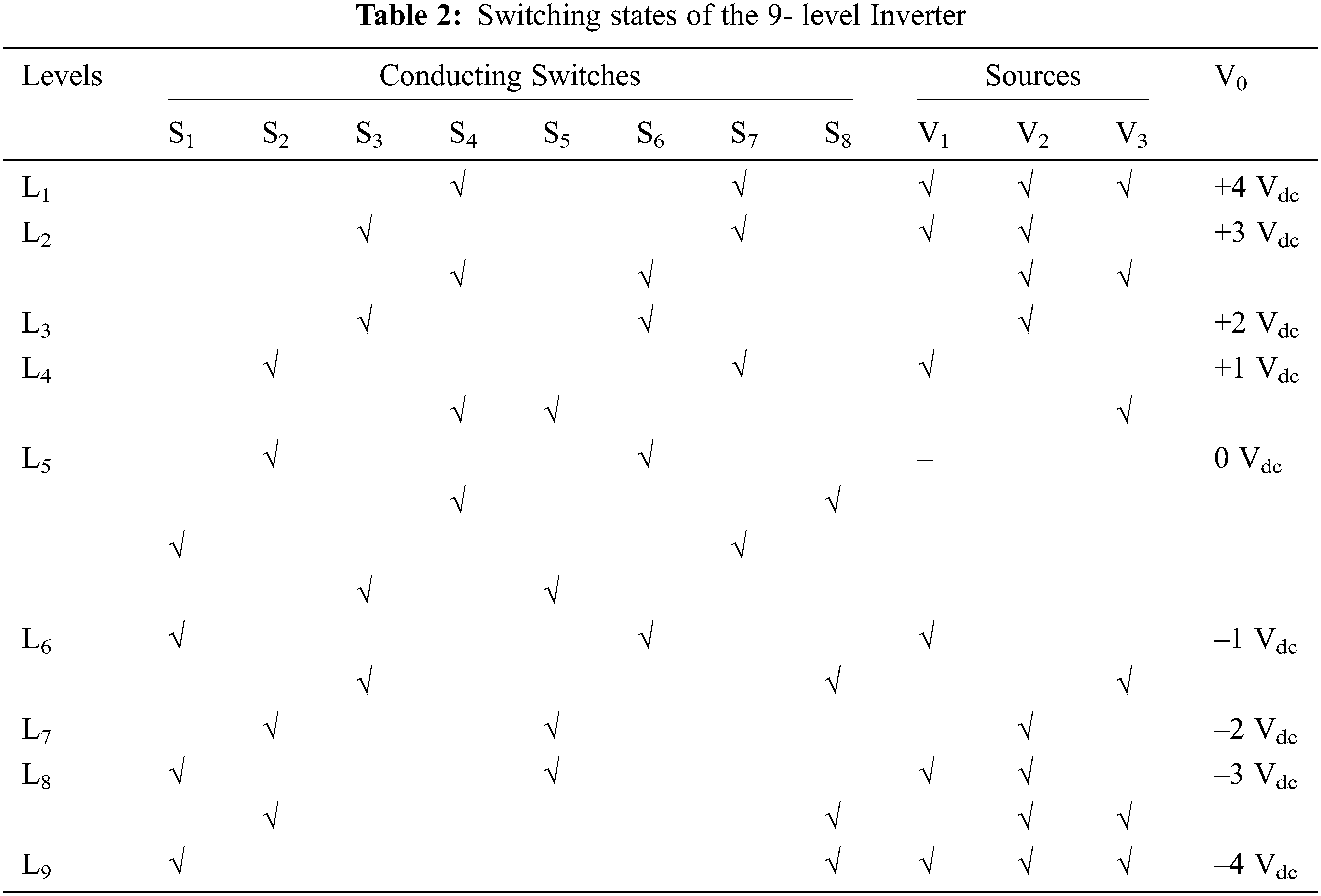
To develop a 9-level MLI, the seven-level inverter topology is enhanced with an addition of one extra DC excitation, and two switches. The developed 9-level MLI consists of eight unidirectional types of switches S1 to S8 and three DC excitations V1, V2, and V3 represented in Fig. 1. The magnitude of voltage for all the sources has opted with various values where the topology is to be termed as asymmetrical type. The DC excitations are selected concerning the ratio of 1:2:1, which are Vdc = V1= 100 V, V2 = 200 V and V3 = 100 V. The switching table for 9–level MLI is represented in Tab. 2. The operation of the 9-level MLI is employed from the respective pulses provided by the switches. For the generation of pulses, the modulation technique used is round-robin staircase type, whereas the activation of the switches is with a symbol `√’, where the switch is turned ON. In other states, the switch becomes turned OFF. The operating modes are represented in Tab. 1, whereas the path of load current is Io. An expected output waveform and several operating modes are denoted in Fig. 2.
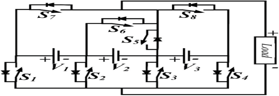
Figure 1: 9-Level asymmetrical MLI structure
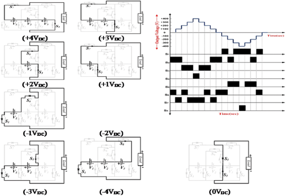
Figure 2: Operating modes and expected output waveform of nine-level MLI topology
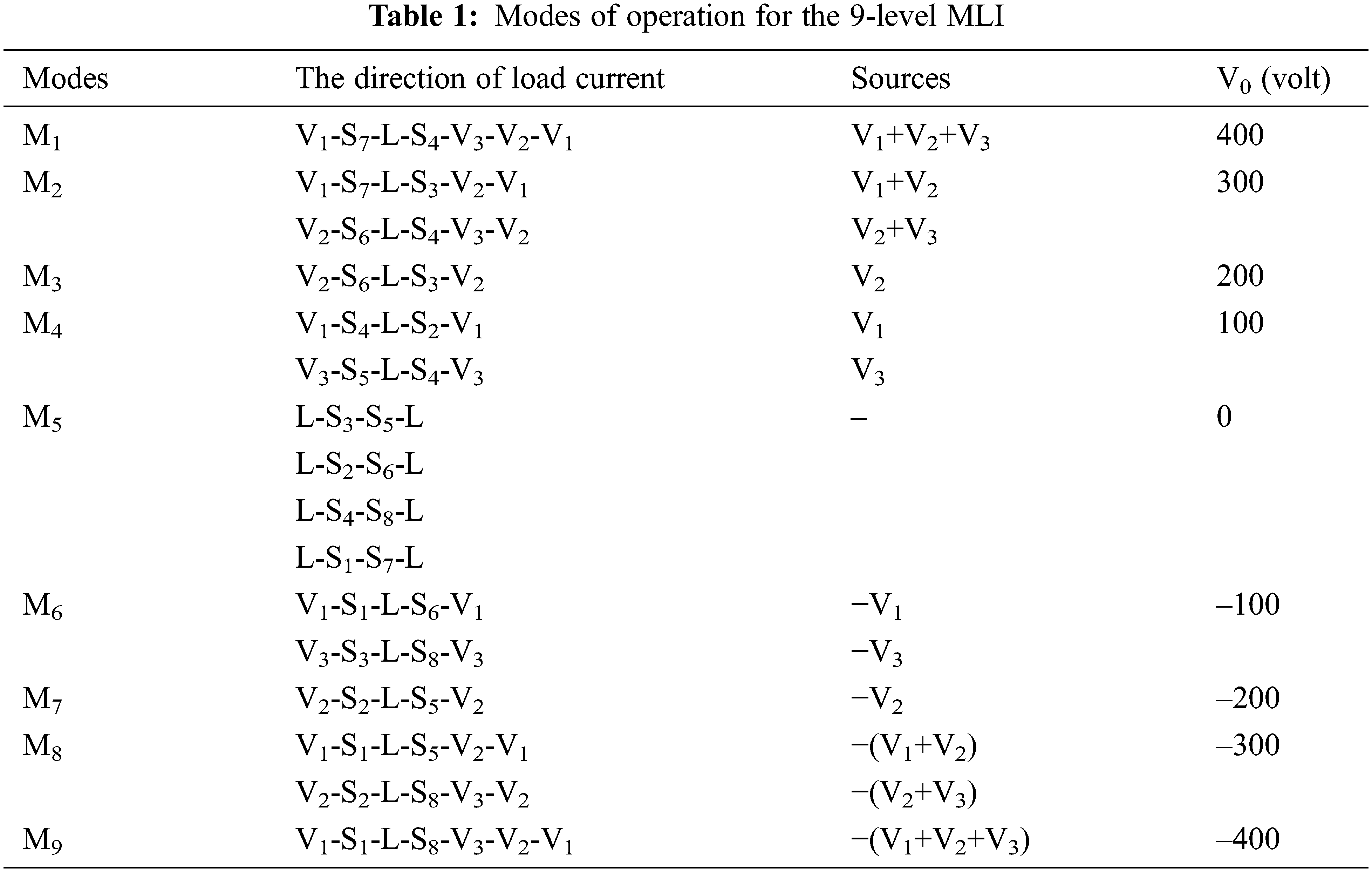
Let ‘p’ be the fundamental units’ count, where P is only one unit
The number of switches NSW is evaluated as Eq. (1)
Number of DC sources NDCS is evaluated as Eq. (2)
Levels count NLEL is evaluated as Eq. (3)
NSW is 8, which is the number of switches, NDCS is 3, DC excitations count and the levels count is NLEL is 9. In mode 1 operation, the switches S4, and S7 conducts and the respective load current Io follows over V1-S7-L-S4-V3-V2-V1, all three sources V1, V2, and V3 excites the network and produces a voltage of +4 Vdc. In the operation of mode 7, the switches S2, and S5 conduct and the respective load current Io path of V2-S2-L-S5-V2, where the source V2 excites the network and produces a voltage of –2 Vdc. In the operation of mode 8, the switches S2, and S8 conducts and the respective load current Io follows the path V2-S2-L-S8-V3-V2, where the sources V1 and V2 excites the network and produces a voltage of –3 Vdc. In the operation of mode 9, the switches S1, and S8 conducts and the load current Io follows the path over V1-S1-L-S8-V3-V2-V1, where all three sources V1, V2, and V3 excite the network and produces a voltage of –4 Vdc.
The 9-level structure is precisely incorporated for addressing various issues that affect the quality of power such as a THD, to have a lesser switches count, the reduced voltage stress on the components i.e., dv/dt stress these features are further enhanced to generate a higher number of levels with fewer switches count, the developed 9-level MLI topology helps in achieving this scenario with less switch count. The simulation output waveforms regarding voltage and currents are represented in Figs. 5 and 6. It is found that the simulation and experimental THD are the same and are represented in Figs. 7 and 10. The developed MLI is experimentally tested in a hardware prototype represented in Fig. 10.
‘√ ’ indicates the conducting switch
3.2 Proposed 17- Level MLI Topology
To develop a 17-level MLI, the nine-level inverter topology is enhanced with an addition of one extra DC excitation, and two switches count. The developed 17-level MLI contains ten unidirectional types of switches S1 to S10 and four DC excitations V1, V2, V3, and V4 represented in Fig. 3. Voltages for all the sources have opted with various values; hence, the developed topology is to be termed asymmetrical. The DC excitations are selected concerning the ratio of 1:2:4:1, which are Vdc = V1 = 50 V, V2 = 100 V, V3 = 200 V, and V4 = 50 V. The switching states for 17 level inverter is represented in Tab. 3.
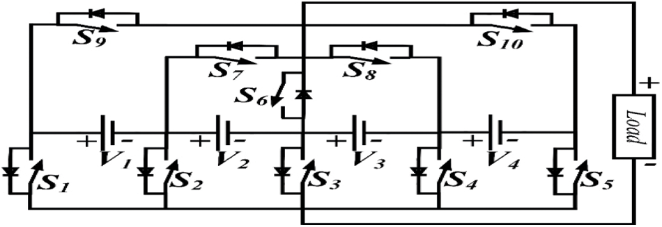
Figure 3: Proposed asymmetrical 17-level MLI topology
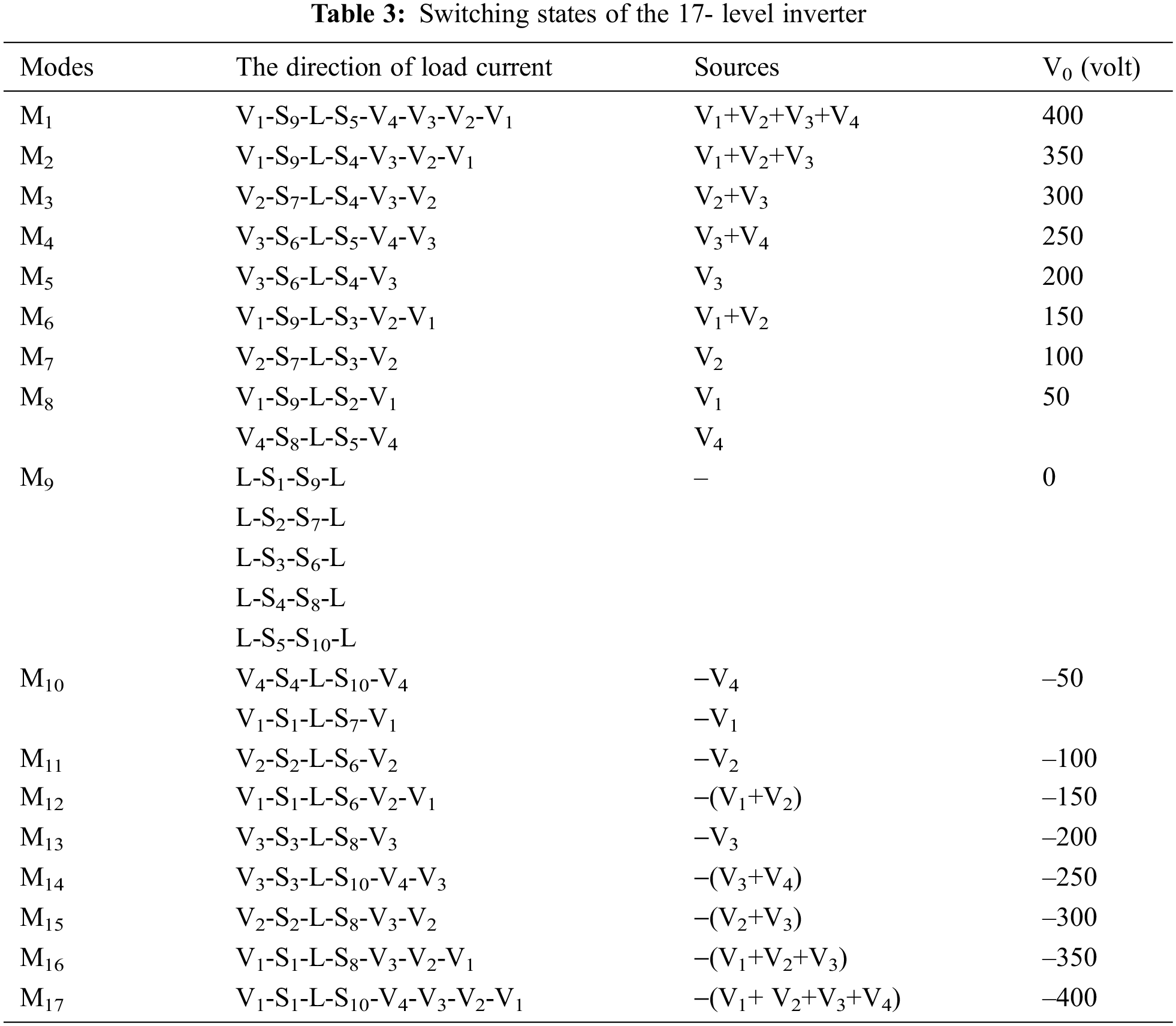
NSW is 10, which is the number of switches, NDCS is 4, the DC excitations count and NLEL is 17, the number of levels. In the operation of mode 1, the switches S5, and S9 conducts and the respective load current Io follows the path V1-S9-L-S5-V4-V3-V2-V1, where the four sources V1, V2, V3, and V4 excite the network and produces a voltage of +8 Vdc. In the operation of mode 2, the switches S4, and S9 conducts and the respective load current Io follows the path V1-S9-L-S4-V3-V2-V1, where the sources V1, V2, and V3 excites the network and produces a voltage of +7 Vdc. In the operation of mode 3, the switches S4, and S7 conducts and the respective load current Io follows the path V2-S7-L-S4-V3-V2, where the sources V2, and V3 excites the network and produces a voltage of +6 Vdc. In the operation of mode 4, the switches S5, and S6 conducts and the respective load current Io follows the path V3-S6-L-S5-V4-V3, where the sources V3 and V4 excites the network and produces a voltage of +5 Vdc. In the operation of mode 5, the switches S4, and S6 conducts and the respective load current Io follows the path V3-S6-L-S4-V3 the source V3 excites the network and produces a voltage of +4 Vdc. In the operation of mode 6, the switches S3, and S9 conducts and the respective load current Io follows the path V1-S9-L-S3-V2-V1, where the sources V1 and V2 excites the network and produces a voltage of +3 Vdc. In the operation of mode 7, the switches S3, and S7 conducts and the respective load current Io follows the path V2-S7-L-S3-V2, where the source V2 excites the network and produces a voltage of +2 Vdc. In the operation of mode 8, the switches S2, and S9 conducts and the respective load current Io follows the path V1-S9-L-S2-V1, where the source V1 excites the network and produces a voltage of +1 Vdc. In the operation of mode 9, the switches S1, and S9 conducts and the respective load current Io follows the path L-S1-S9-L, where the excitation is absent in this scenario and generates a voltage of is 0 Vdc.
The 17-level MLI operation is employed from the pulses provided by switches. For the generation of pulses, the modulation technique used is round-robin staircase type, whereas the activation of the switches is with a symbol `√’, where the switch is turned ON. In other states, the switch becomes turned OFF. The respective operating modes of the 17-level MLI along with the load current path Io whereas the switching states are represented in Tab. 3. The expected output waveform and several operating modes of the proposed 17-level structure are exposed in Fig. 4.
Figure 4: Operating modes and expected output waveform of seventeen level MLI topology
Let ‘p’ be the fundamental units’ count, where P is only one unit
The number of switches NSW is evaluated as Eq. (4)
Several DC sources NDCS is evaluated as Eq. (5)
Levels count NLEL is evaluated as Eq. (6)
In the operation of mode 10, the switches S1, and S7 conducts and the respective load current Io follows the path V1-S1-L-S7-V1, where the source V1 excites the network and produces a voltage of –1Vdc. In the operation of mode 11, the switches S2, and S6 conducts and the respective load current Io follows the path V2-S2-L-S6-V2, where the source V2 excites the network and produces a voltage of –2 Vdc. In the operation of mode 12, the switches S1, and S6 conducts and the respective load current Io follows the path V1-S1-L-S6-V2-V1, where the sources V1, and V2 excites the network and produces a voltage of –3 Vdc.
In the operation of mode 13, the switches S3, and S8 conducts and the respective load current Io follows the path V3-S3-L-S8-V3, where the source V3 excites the network and produces a voltage of –4 Vdc. In the operation of mode 14, the diode D2 and switches S3, and S10 conducts and the respective load current Io follows the path V3-S3-L-S10-V4-V3, where the sources V3, and V4 excites the network and produces a voltage of –5 Vdc. In the operation of mode 15, the switches S2, and S8 conducts and the respective load current Io follows the path V2-S2-L-S8-V3-V2, where the sources V2 and V3 excites the network and produces a voltage of –6 Vdc. In the operation of mode 16, the switches S1, and S8 conducts and the respective load current Io follows the path V1-S1-L-S8-V3-V2-V1, where the sources V1, V2, and V3 excites the network and produces a voltage of –7 Vdc. In the operation of mode 17, the switches S1, and S10 conducts and the respective load current Io follows the path V1-S1-L-S10-V4-V3-V2-V1, where the sources V1, V2, V3, and V4 excites the network and produces a voltage of –8 Vdc. The 17-level structure is precisely incorporated for addressing various issues that affect the quality of power such as a THD, to have a lesser switches count, the reduced voltage stress on the components i.e., dv/dt stress these features are further enhanced to produce a higher number of levels with fewer switches count, the developed 17-level MLI topology helps in achieving this scenario with less switch count. The simulation output waveforms regarding currents and voltage are represented in Fig. 14. An experimental output with R-load is exposed in Fig. 15. It appears that that the simulation and experimental THD are the same and are represented in Figs. 13 and 16. An experimental output current and a voltage waveform of 9 levels MLI is exposed in Figs. 8 and 9.
The result and discussions of different levels of MLI are as follows,
A proposed simulation 9-level MLI structure is done in MATLAB/Simulink, whereas, a generation of switching pulses can be done at 2 kHz frequency and is related with a frequency of 50Hz, the structure is precisely tested for the resistive load of 100 Ω, the maximum voltage of 400 V is obtained via provide input DC sources Vdc = V1 = 100 V, V2 = 200 V, and V3 = 100 V respectively. Figs. 8 and 9 represent an outcome of simulation results such as current and voltage waveforms of the developed 9-level MLI topology, respectively. From Fig. 5 and 6, it concludes that the maximum peak voltage is 400 V and the respective load current is 4 A.
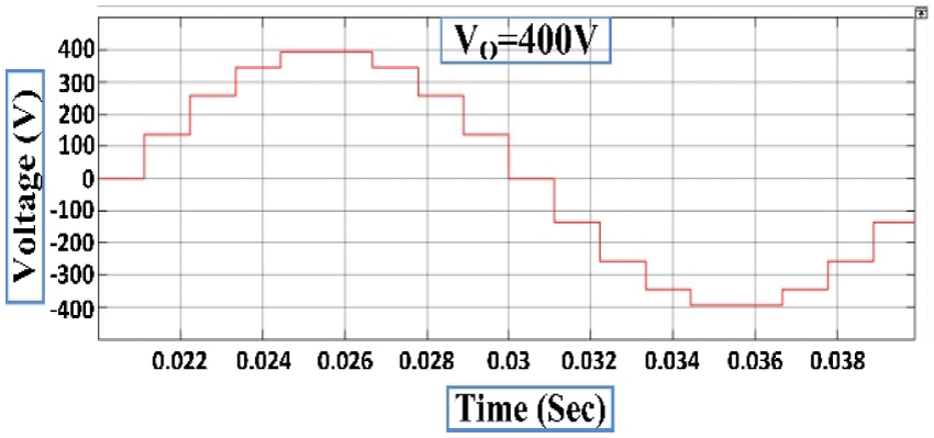
Figure 5: Simulation output voltage
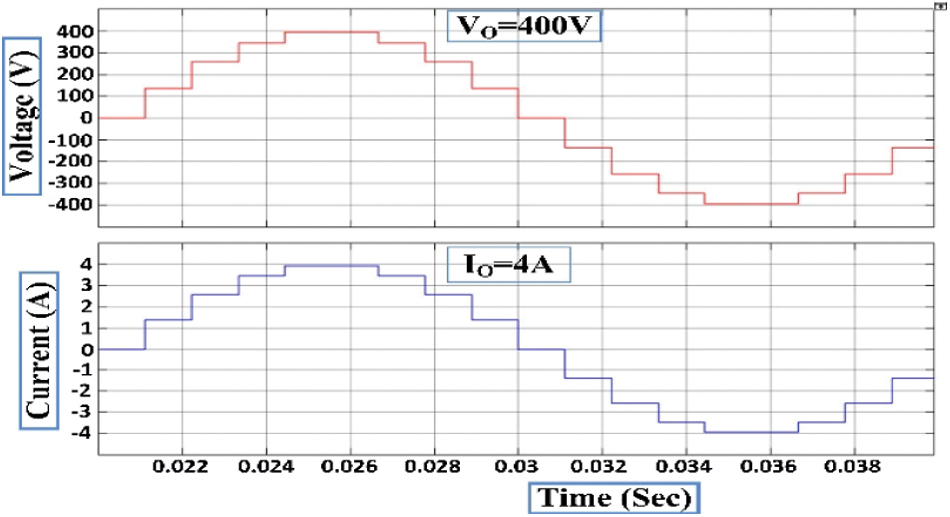
Figure 6: Simulation voltage and current waveform of 9-level MLI
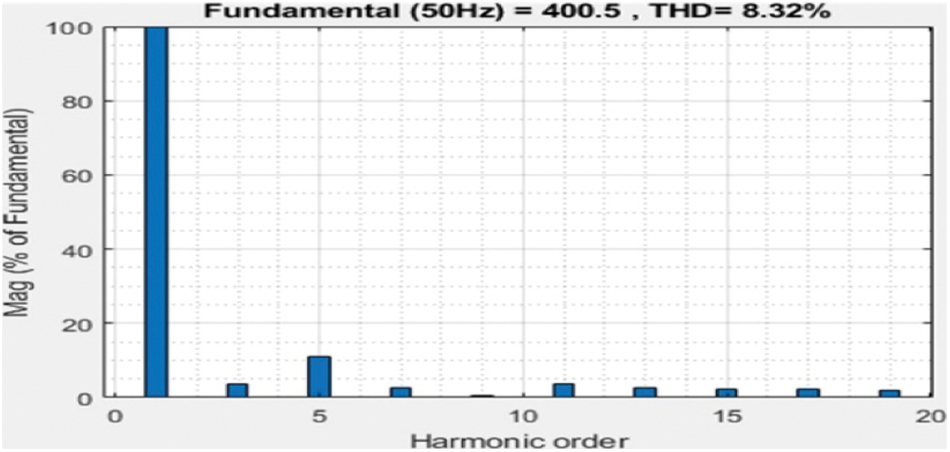
Figure 7: Simulation THD of 9 level MLI
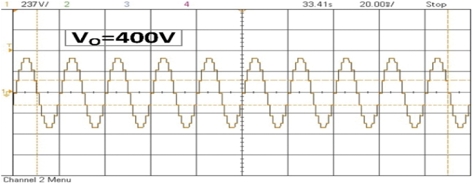
Figure 8: Experimental voltage waveform of 9-level MLI
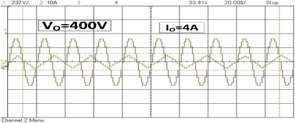
Figure 9: Experimental output voltage and current waveform of 9 level MLI
A proposed asymmetrical topology of the 9-level MLI structure is proved experimentally using a setup in the laboratory shown in Fig. 10. An inverter modeled setup used CM75DU-12H IGBT which are fed with MCT2E optocouplers, three exists three unequal DC excitations with V1 = 100 V, V2 = 200 V, and V3 = 100 V, 100 Ω R-load then the generation of pulses can be done from dSPACE RTI1104. The hardware prototype with R-Load under SteadyState output voltage V0 = 400 V is 282.84 Vrms, load current I0 = 4 A, which is 2.82 A Irms the THD value measured is 8.32% by using with power analyzer and is voltage represented in Fig. 7.
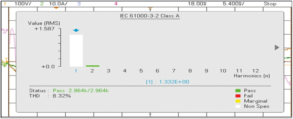
Figure 10: Experimental THD of 9-level MLI
A proposed simulation 17-level MLI structure is done in MATLAB/Simulink, whereas the generation of switching pulses can be done at 2 kHz frequency and is compared with a frequency of 50 Hz, the structure is precisely tested for the resistive load of 100 Ω, the maximum voltage of 400 V is obtained via providing input DC sources Vdc = V1 = 50 V, V2 = 100 V, V3 = 200 V, and V4 = 50 V respectively. Figs. 11 and 12 represent outcomes of simulation results such as Current and Voltage waveforms of the developed 17-level MLI topology, respectively. From Figs. 11 and 12, it is found that the maximum peak voltage is 400 V and the respective load current is 4 A. A simulation THD is shown in Fig. 13. The proposed asymmetrical topology of the 17-level MLI structure is proved experimentally using a setup in the laboratory. The setup of inverter modeled using CM75DU-12H IGBT which are fed with MCT2E optocouplers, three exists four unequal DC excitations with V1 = 50 V, V2 = 100 V, V3 = 200 V, and V4 = 50 V, R-load with a value of 100 Ω and the generation of pulses can be done from dSPACE RTI1104. The hardware prototype with R-Load under SteadyState output voltage V0 = 400 V is 282.84 Vrms, load current I0 = 4A which is 2.82 A Irms for R-load and V0 = 400 V is 282.84 Vrms, load current I0 = 6.8A which is 4.8A Irms for RL-load are shown in Figs. 14 & 15 respectively. The THD value measured is 4.14% by using a power analyzer and is represented in Fig. 16.
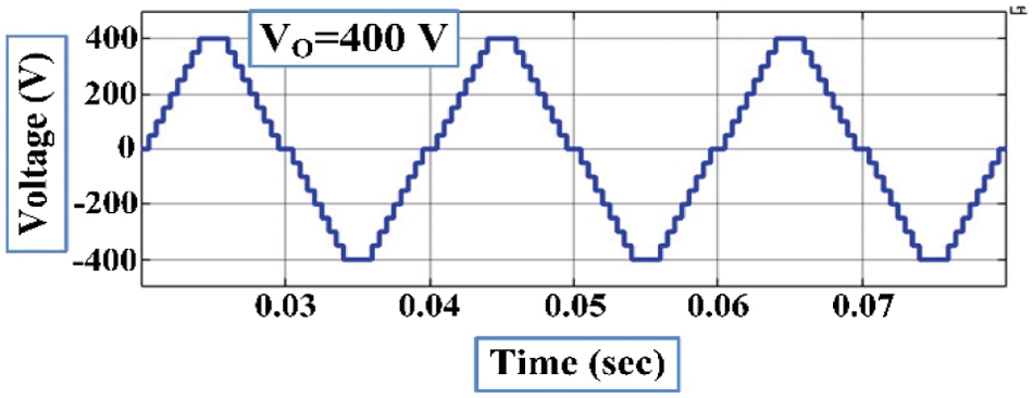
Figure 11: Simulation output voltage of 17 levels MLI
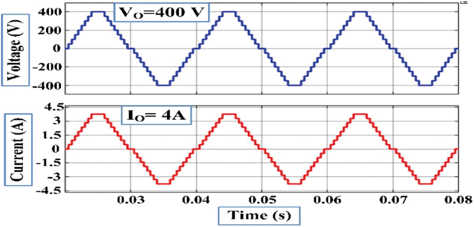
Figure 12: Simulation voltage & current waveform of 17 levels MLI
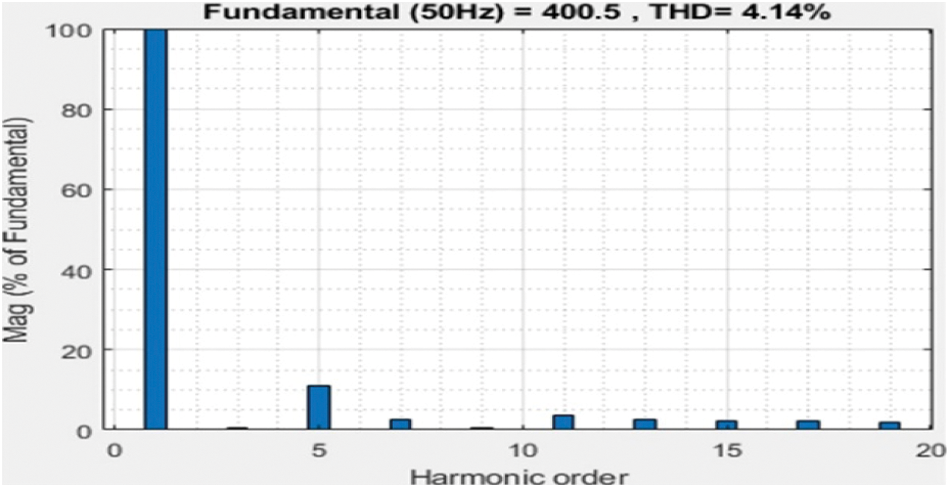
Figure 13: Simulation THD of 17 levels MLI
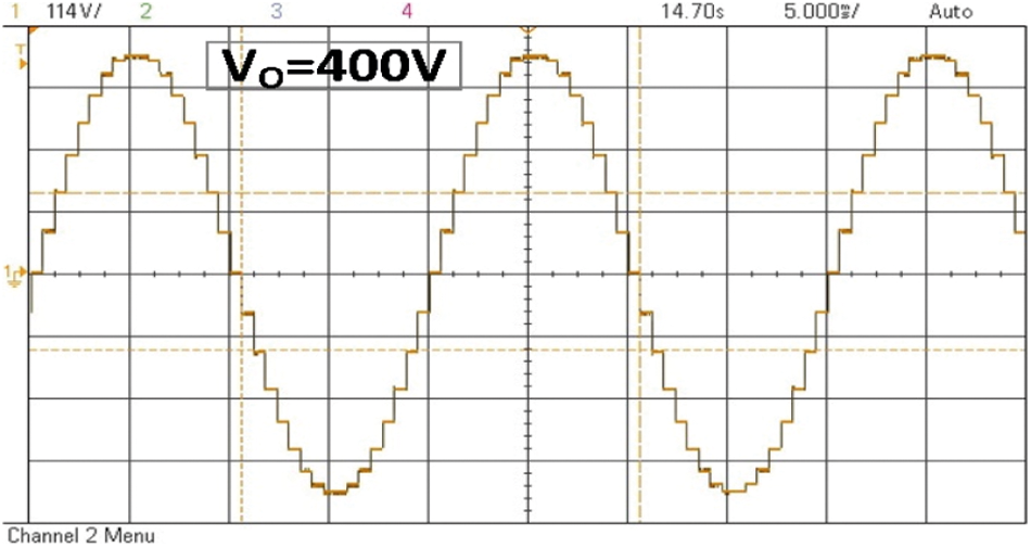
Figure 14: Experimental voltage waveform 17 levels MLI
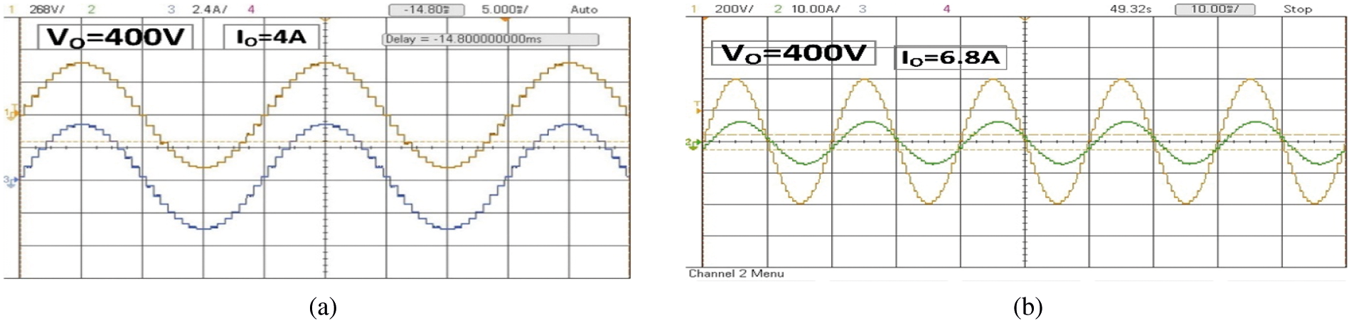
Figure 15: Experimental voltage and current waveform of 17 level MLI for (a) R-load (b) RL-load
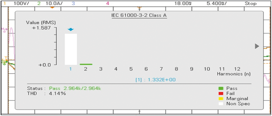
Figure 16: Experimental THD of 17 levels MLI
5 Calculations and Comparative Studies
The entire inefficiencies are categorized under two groups: conduction and switching losses, both of that are intimately tied toward the switching devices.
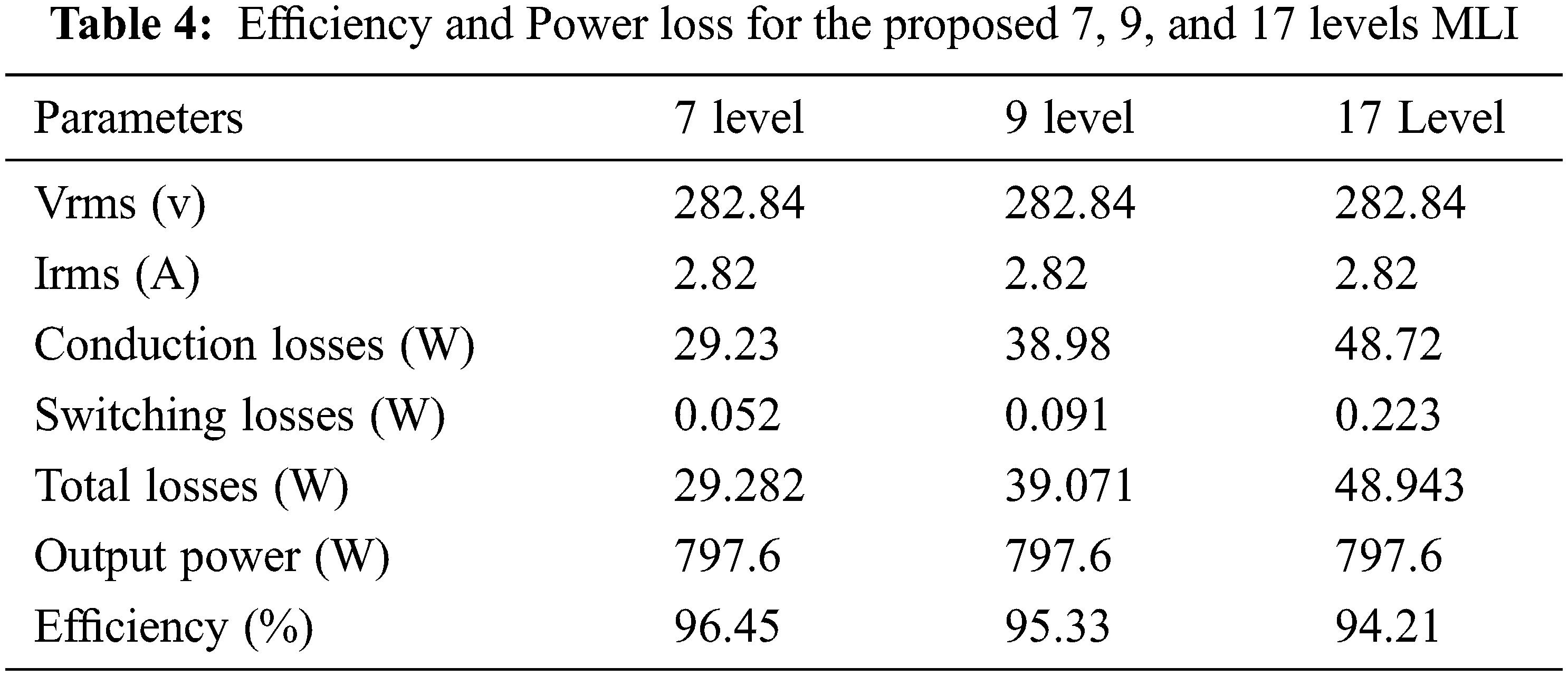
Conduction losses contribute a significant role in these losses anytime the switch is turned on at any time, hence conduction losses are calculated using the following formula. Eq. (7) and the overall MLI for efficiency and total power loss for the proposed 7, 9, and 17 levels MLI is tabulated in Tab. 4
where, VS is the voltage across the IGBT switch. The resistance of the switch is represented as
The calculation of switching losses can be done using the following relation Eq. (8)
where Eon and Eoff are the utilized energies by the switches under conduction state.
The overall power losses (Ptotal loss) are calculated according to the following relation Eq. (9)
Overall topology efficiency (ɳ) can be determined used the following Eq. (10)
where, Pout and Pin are the respective powers of output and input.
Respective output power can be determined using Eq. (11)
5.2 Total Standing Voltage (TSV)
A multilayer inverter's cumulative standing voltage is crucial in obtaining the greatest blocking voltage over the individual switches. It is an important issue to consider while choosing switches. To get the TSV value, all of the respective maximal blocking voltages over the switches are added together. The tension over the switch is represented by the amount of blocking voltage. A voltage stress changes depending on the switch type, including bi-directional and unidirectional switches. As a result, the voltage stress on bidirectional and unidirectional switches is determined: VSbi = Vi and VSuni = 2 Vi respectively, where i = 1, 2, 3……n number of complementary switches. Concerning the tertiary operating mode, the maximum output voltage (VO, MAX) is
In the developed MLI, voltages are equal for the switches that are in the complementary design and here, all the switches are unidirectional. Therefore, TSV determined from the below equations:
For 9-level MLI.
For 17-level MLI.
The TSV per unit (TSVpu) can be calculated by Eq. (12).
A cost function may be used to evaluate the economic assessments for the construction of MLI. A cost function for the proposed 9, and 17-level MLI may be calculated using several factors such as NSW, the number of switches, NDCS, the number of sources, ND, the number of diodes, ND, the number of capacitors, NC, TSV, NDK, the number of driver circuits, and the number of sources NSDC. As a result, the cost factor is calculated using the Eq. (13) and the formula below [39].
where ‘α’ is the weight coefficient. Generally, the value of α is greater than 1 and less than unity. In the proposed MLI, the value of α is analyzed as 0.5 (<1) and 1.5 (>1) for the optimal calculation of the cost factor. The MLI is found to be cost-effective based on the calculation of component level count (CF/L).
The total components utilized in the topology can be determined by using component level factor and is calculated using the Eq. (14).
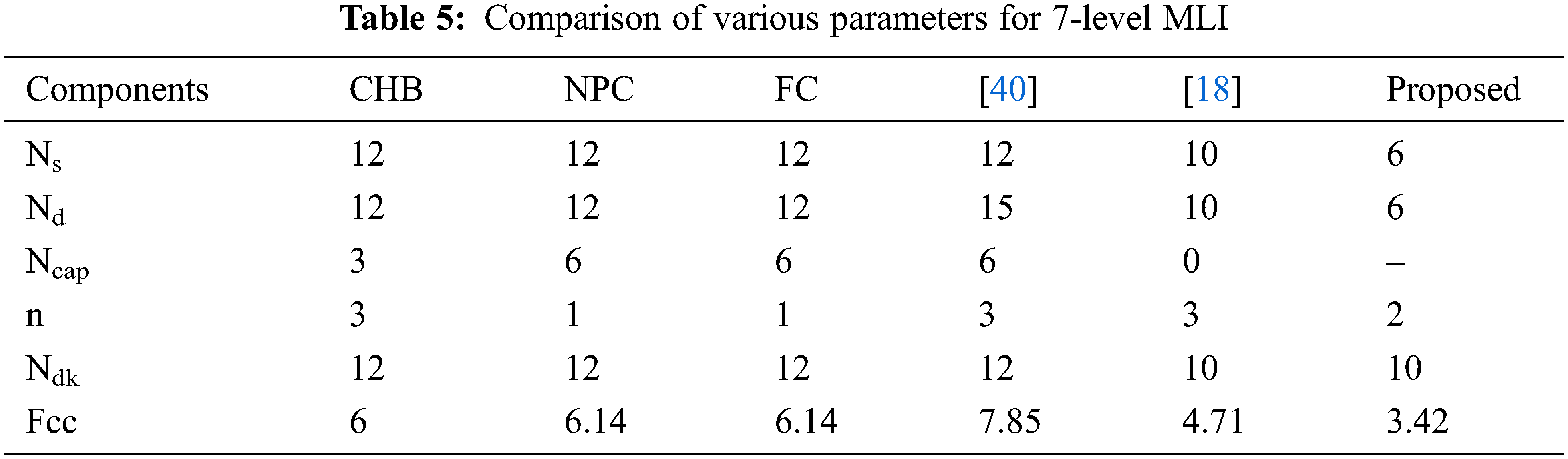
A detailed comparison is done on various parameters used in the process of realization such as switches count NSW, diodes count ND, driver circuits count NDK, capacitors count NC, the total standing voltage per unit TSVPU, voltage sources count NSDC, components count factor CC/L with a cost function per level CF/L.
The 7-level structure compared with the existing and modern topologies is precisely done then tabulated in Tab. 5 and the respective graphical representations are represented in Fig. 17. Similarly, the respective comparisons of 9-level and 17-level MLI with several parameters are done and are compared with the traditional and modern topologies and are represented in Tab. 6 and Tab. 7 respectively, where the graphical representations are exposed in Figs. 18 and 19 respectively.
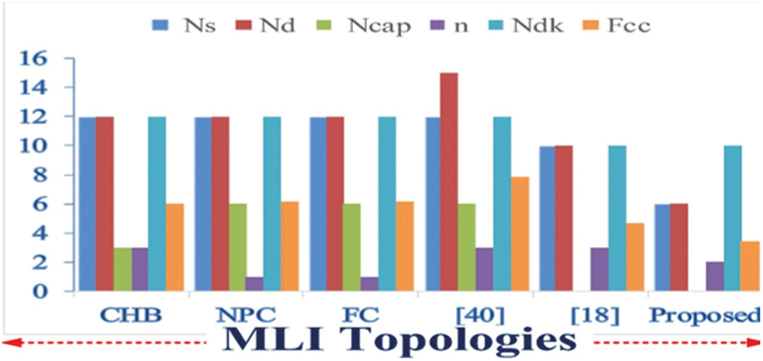
Figure 17: Comparison of parameter for 7-level MLI topology with existing topologies
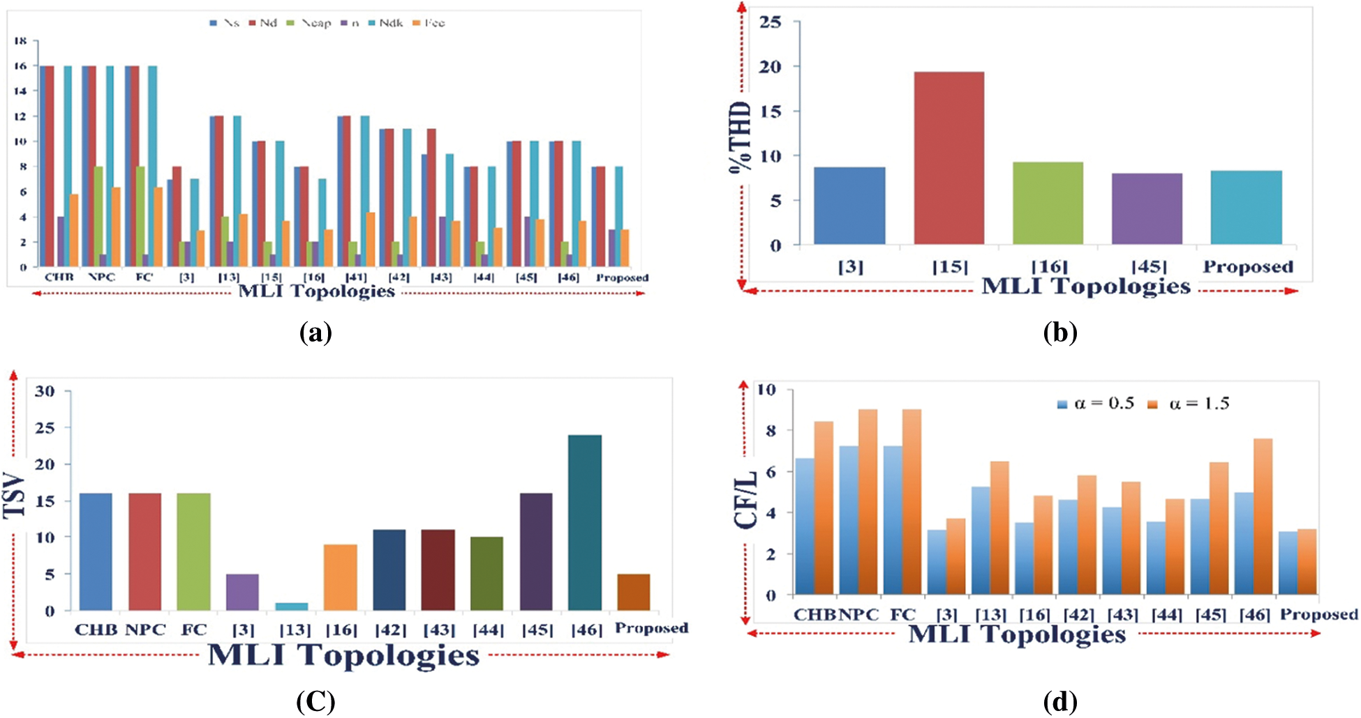
Figure 18: Comparison of parameters for 9-level MLI topology with (a) Ns, Nd, Ncap, n, Ndk, Fcc (b) %THD (c) TSV and (d) CF/L
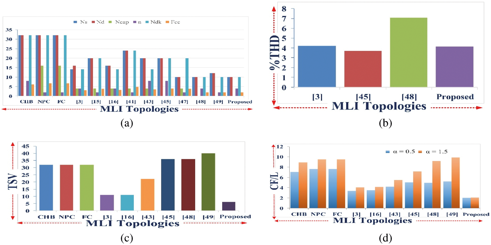
Figure 19: Comparison of parameters for 17-level MLI topology with (a) Ns, Nd, Ncap, n, Ndk, Fcc (b) %THD (c) TSV and (d) CF/L
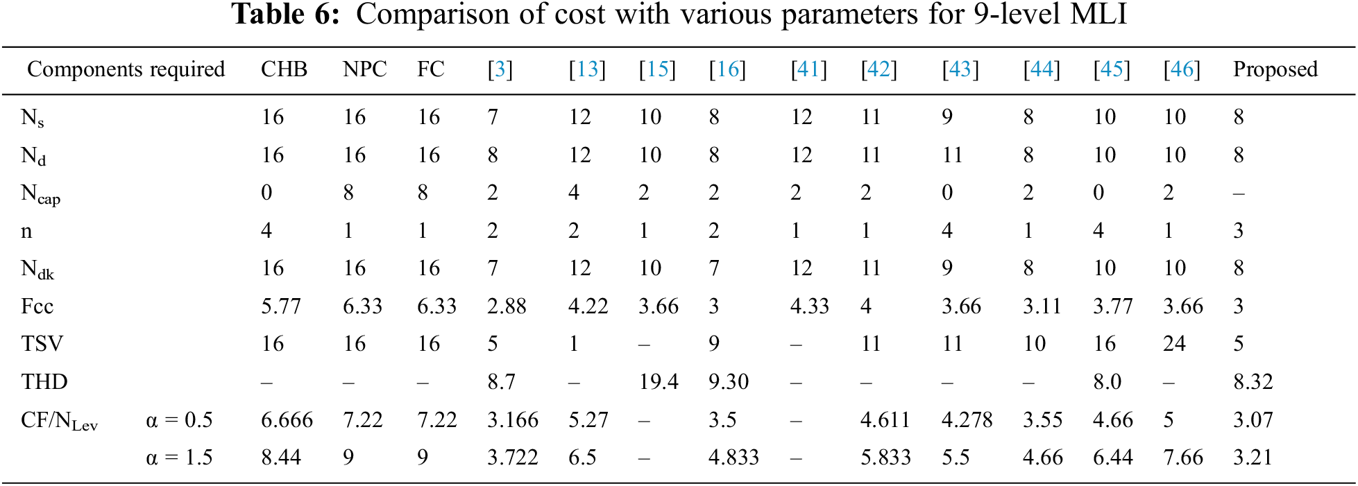
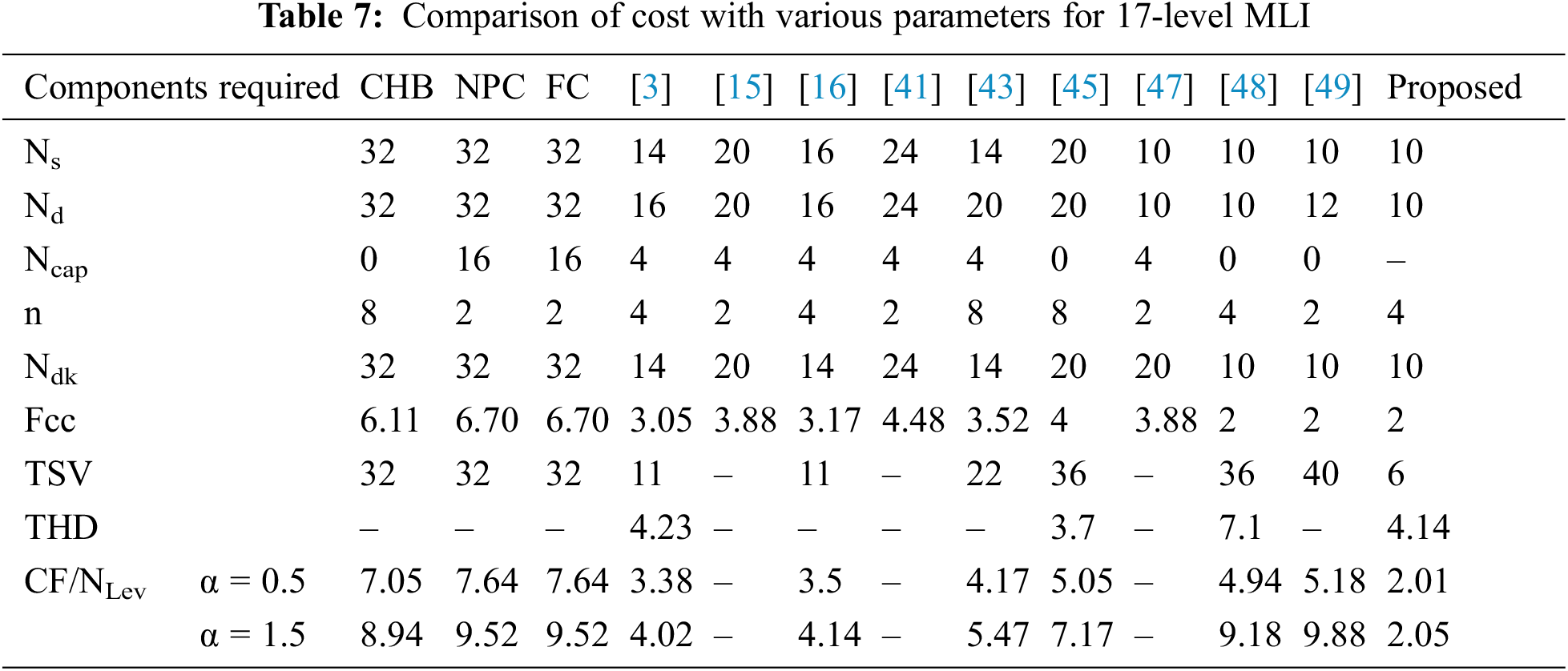
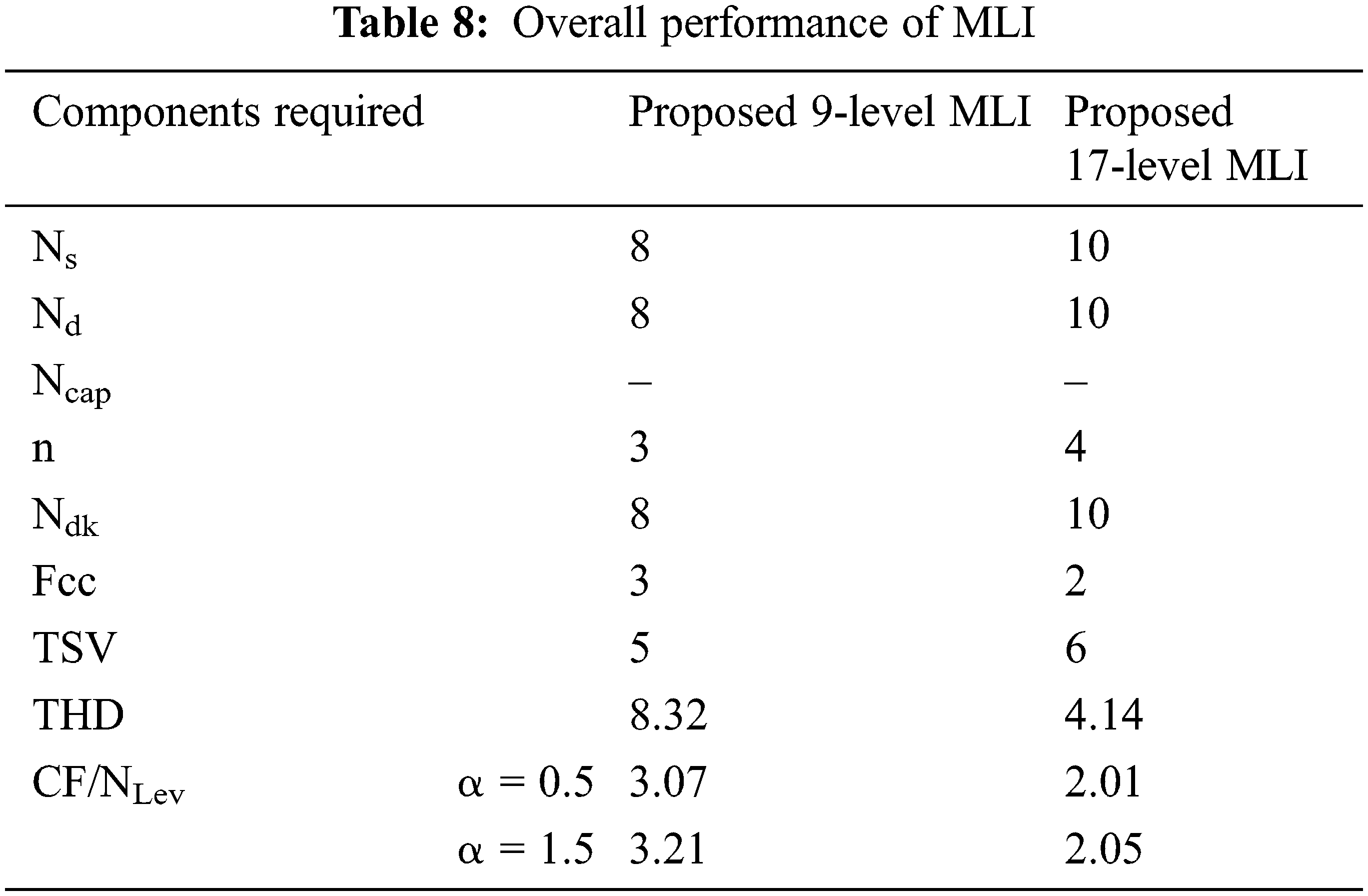
Overall performance of MLI proposed method in represented by Tab. 8. where the graphical representations are shown in Fig. 20 respectively.
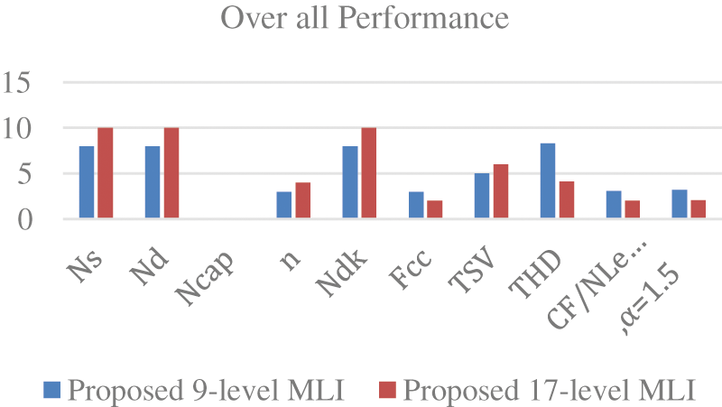
Figure 20: Overall Performance of MLI
A new asymmetrical 17-level MLI structure is established from the basic 7-level and 9-level MLI topologies. The basic 7-level MLI and 9-level MLI are realized with several parameters and further developed to 17-level MLI. The developed MLI consists of fewer components, due to which the size and cost of the inverter get compact. Therefore, the reliability and efficiency of the proposed MLI get improved. The MLI requires a lesser component to deliver expected output voltage levels with less THD. Also, the TSV and respective cost factor is calculated and found to be cost-effective. Various comparisons are made concerning the several parameters with various conventional and modern pre-existing topologies. The comparisons prove that a developed MLI is very much efficient and there exists less utilization of power. Also, it is observed that the results obtained in both simulation and experimental THD are the same and are 4.14%. The TSV is 6 Vdc, efficiency is 94.21% and cost factor per level CF/L value for both values of α is 2.01 and 2.05 respectively, representing a developed MLI is cost-effective with all existing topologies. A developed MLI is verified with load variations with resistive load and inductive load and the combinational loads and found to be stable. Future scope of the proposed work can be obtained by improving the efficiency of the inverter by addition of further Level to 18 or 19.
Acknowledgement: The author with a deep sense of gratitude would thank the supervisor for his guidance and constant support rendered during this research.
Funding Statement: The authors received no specific funding for this study.
Conflicts of Interest: The authors declare that they have no conflicts of interest to report regarding the present study.
1. G. Ramya, V. Ganapathy and P. Suresh, “Comprehensive analysis of interleaved boost converter with simplified H-bridge multilevel inverter based static synchronous compensator system,” Electric Power Systems Research, vol. 176, no. 2, pp. 105936, 2019. [Google Scholar]
2. R. Sepehrzad, M. E. Hassanzadeh, A. R. Seifi and M. Mazinani, “An efficient multilevel interconnect control algorithm in AC/DC micro-grids using hybrid energy storage system,” Electric Power Systems Research, vol. 191, no. 4, pp. 106869, 2021. [Google Scholar]
3. C. Dhanamjayulu, D. Prasad, S. Padmanaban, P. K. Maroti, J. B. Holm-Nielsen et al., “Design and implementation of seventeen level inverter with reduced components,” IEEE Access, vol. 9, pp. 16746–16760, 2021. [Google Scholar]
4. C. M. Freitas, E. H. Watanabe and L. F. C. Monteiro, “A linearized small-signal Thevenin-equivalent model of a voltage-controlled modular multilevel converter,” Electric Power Systems Research, vol. 182, pp. 106231, 2020. [Google Scholar]
5. H. A. Khalid, N. A. A. Emadi, L. B. Brahim, A. Gastli and C. Cecati, “A novel control scheme for three-phase seven-level packed U-Cell based DSTATCOM,” Electric Power Systems Research, vol. 182, no. 1, pp. 106201, 2020. [Google Scholar]
6. S. R. Khasim, C. Dhanamjayulu, S. Padmanaban, J. B. H. Nielsen and M. Mitolo, “A novel asymmetrical 21-level inverter for solar PV energy system with reduced switch count,” IEEE Access, vol. 9, pp. 11761–11775, 2021. [Google Scholar]
7. S. Umashankar, T. S. Sreedevi, V. G. Nithya and D. Vijayakumar, “A new 7-level symmetric multilevel inverter with minimum number of switches,” International Scholarly Research Notices, vol. 2013, no. 11, pp. 1–9, 2013. [Google Scholar]
8. K. S. Suresh and M. V. Prasad, “Analysis and simulation of new seven level inverter topology,” International Journal of Scientific and Research Publications, vol. 2, no. 4, pp. 1–6, 2012. [Google Scholar]
9. R. Choupan, S. Golshannavaz, D. Nazarpour and M. Barmala, “A new structure for multilevel inverters with fault-tolerant capability against open circuit faults,” Electric Power Systems Research, vol. 168, no. 1, pp. 105–116, 2019. [Google Scholar]
10. B. Sharma, R. Dahiya and J. Nakka, “Effective grid connected power injection scheme using multilevel inverter-based hybrid wind solar energy conversion system,” Electric Power Systems Research, vol. 171, pp. 1–14, 2019. [Google Scholar]
11. Z. Zhao, Y. Li and B. Dong, “Modelling and control strategy for cascade bi-directional DC/DC converter in microgrid,” in Proc. Int. Power Electronics and Motion Control Conf., Harbin, China, IEEE, vol.3, pp. 1747–1751, 2012. [Google Scholar]
12. S. Eren, A. Bakhshai and P. Jain, “Control of three-phase voltage source inverter for renewable energy applications,” in Proc. Int. Telecommunications Energy Conf., Amsterdam, Netherlands, IEEE, pp. 1–4, 2011. [Google Scholar]
13. S. S. Lee, C. S. Lim and K. B. Lee, “Novel active-neutral-point-clamped inverters with improved voltage-boosting capability,” IEEE Transactions on Power Electronics, vol. 35, no. 6, pp. 5978–5986, 2019. [Google Scholar]
14. A. P. Patel, V. J. Rupapara and A. R. Gauswami, “Design and simulation of 9-level hybrid cascaded H-bridge multilevel inverter with reduced components,” in Proc. Int. Conf. on Current Trends towards Converging Technologies, Coimbatore, India, IEEE, pp. 1–7, 2018. [Google Scholar]
15. A. Tirupathi, K. Annamalai and S. V. Tirumala, “A new hybrid flying capacitor-based single-phase nine-level inverter,” International Transactions on Electrical Energy Systems, vol. 29, no. 12, pp. 12139, 2019. [Google Scholar]
16. P. Bhatnagar, R. Agrawal and K. K. Gupta, “Reduced device count version of single-stage switched-capacitor module for cascaded multilevel inverters,” IET Power Electronics, vol. 12, no. 5, pp. 1079–1086, 2019. [Google Scholar]
17. M. D. Siddique, S. Mekhilef, N. M. Shah, A. Sarwar, A. Iqbal et al., “A new multilevel inverter topology with reduce switch count,” IEEE Access, vol. 7, pp. 58584–58594, 2019. [Google Scholar]
18. C. Dhanamjayulu, S. R. Khasim, S. Padmanaban, G. Arunkumar, J. B. H. Nielsen et al., “Design and implementation of multilevel inverters for fuel cell energy conversion system,” IEEE Access, vol. 8, pp. 183690–183707, 2020. [Google Scholar]
19. K. K. Gupta, A. Ranjan, P. Bhatnagar, L. K. Sahu and S. Jain, “Multilevel inverter topologies with reduced device count: A review,” IEEE Transactions on Power Electronics, vol. 31, no. 1, pp. 135–151, 2015. [Google Scholar]
20. W. K. Choi and F. S. Kang, “H-bridge based multilevel inverter using PWM switching function,” in Int. Telecommunications Energy Conf., Incheon, Korea (SouthIEEE, pp. 1–5, 2009. [Google Scholar]
21. K. K. Gupta and S. Jain, “Topology for multilevel inverters to attain maximum number of levels from given DC sources,” IET Power Electronics, vol. 5, no. 4, pp. 435–446, 2012. [Google Scholar]
22. H. Vahedi and K. A. Haddad, “Half-bridge based multilevel inverter generating higher voltage and power,” in Proc. IEEE Electrical Power & Energy Conf., Halifax, NS, Canada, IEEE, pp. 1–6, 2013. [Google Scholar]
23. C. Dhanamjayulu, G. Arunkumar, B. J. Pandian and S. Padmanaban, “Design and implementation of a novel asymmetrical multilevel inverter optimal hardware components,” International Transactions on Electrical Energy Systems, vol. 30, no. 2, pp. 12201, 2020. [Google Scholar]
24. K. K. Gupta and S. Jain, “A novel multilevel inverter based on switched DC sources,” IEEE Transactions on Industrial Electronics, vol. 61, no. 7, pp. 3269–3278, 2013. [Google Scholar]
25. C. Dhanamjayulu and S. Meikandasivam, “Fuzzy controller-based design of 125 level asymmetric cascaded multilevel inverter for power quality improvement,” Analog Integrated Circuits and Signal Processing, vol. 101, no. 3, pp. 533–542, 2019. [Google Scholar]
26. E. Babaei, M. F. Kangarlu and F. N. Mazgar, “Symmetric and asymmetric multilevel inverter topologies with reduced switching devices,” Electric Power Systems Research, vol. 86, no. 3, pp. 122–130, 2012. [Google Scholar]
27. J. S. Choi and F. S. Kang, “Seven-level PWM inverter employing series-connected capacitors paralleled to a single DC voltage source,” IEEE Transactions on Industrial Electronics, vol. 62, no. 6, pp. 3448–3459, 2014. [Google Scholar]
28. A. Emadi, S. S. Williamson and A. Khaligh, “Power electronics intensive solutions for advanced electric, hybrid electric, and fuel cell vehicular power systems,” IEEE Transactions on Power Electronics, vol. 21, no. 3, pp. 567–577, 2006. [Google Scholar]
29. D. Prasad, C. Dhanamjayulu, S. Padmanaban, J. B. H. Nielsen, F. Blaabjerg et al., “Design and implementation of 31-level asymmetrical inverter with reduced components,” IEEE Access, vol. 9, pp. 22788–22803, 2021. [Google Scholar]
30. C. Dhanamjayulu, S. Padmanaban, J. B. H. Nielsen and F. Blaabjerg, “Design and implementation of a single-phase 15-level inverter with reduced components for solar PV applications,” IEEE Access, vol. 9, pp. 581–594, 2020. [Google Scholar]
31. A. Khodaparast, E. Azimi, A. Azimi, M. E. Adabi, J. Adabi et al., “A new modular multilevel inverter based on step-up switched-capacitor modules,” Energies, vol. 12, no. 3, pp. 524, 2019. [Google Scholar]
32. J. S. M. Ali, D. J. Almakhles, S. A. Ibrahim, S. Alyami, S. Selvam et al., “A generalized multilevel inverter topology with reduction of total standing voltage,” IEEE Access, vol. 8, pp. 168941–168950, 2020. [Google Scholar]
33. M. D. Siddique, S. Mekhilef, M. Rawa, A. Wahyudie, B. Chokaev et al., “Extended multilevel inverter topology with reduced switch count and voltage stress,” IEEE Access, vol. 8, pp. 201835–201846, 2020. [Google Scholar]
34. M. H. Mondol, M. R. Tür, S. P. Biswas, M. K. Hosain, S. Shuvo et al., “Compact three phase multilevel inverter for low and medium power photovoltaic systems,” IEEE Access, vol. 8, pp. 60824–60837, 2020. [Google Scholar]
35. J. Ebrahimi, E. Babaei and G. B. Gharehpetian, “A new multilevel converter topology with reduced number of power electronic components,” IEEE Transactions on Industrial Electronics, vol. 59, no. 2, pp. 655–667, 2011. [Google Scholar]
36. A. Ruderman, G. Mehlmann and B. Reznikov, “PWM voltage quality bounds of a single-phase multilevel converter,” in Proc. Int. Conf. on Optimization of Electrical and Electronic Equipment, Brasov, Romania, IEEE, pp. 783–789, 2012. [Google Scholar]
37. M. D. Siddique, S. Mekhilef, A. Sarwar, A. Alam and N. M. Shah, “Dual asymmetrical dc voltage source based switched capacitor boost multilevel inverter topology,” IET Power Electronics, vol. 13, no. 7, pp. 1481–1486, 2020. [Google Scholar]
38. C. Dhanamjayulu, S. Padmanaban, V. K. Ramachandaramurthy, J. B. H. Nielsen and F. Blaabjerg, “Design and implementation of multilevel inverters for electric vehicles,” IEEE Access, vol. 9, pp. 317–338, 2020. [Google Scholar]
39. S. Sabyasachi, V. B. Borghate and S. K. Maddugari, “A 21-level bipolar single-phase modular multilevel inverter,” Journal of Circuits, Systems and Computers, vol. 29, no. 1, pp. 2050004, 2020. [Google Scholar]
40. S. Birundha and V. Saravanan, “Design and development of Z source cascaded seven level inverter for solar photovoltaic system,” in Proc. Int. Conf. on Computation of Power, Energy, Information and Communication, Melmaruvathur, India, IEEE, pp. 0087–0092, 2015. [Google Scholar]
41. S. S. Lee, “Single-stage switched-capacitor module (S 3 CM) topology for cascaded multilevel inverter,” IEEE Transactions on Power Electronics, vol. 33, no. 10, pp. 8204–8207, 2018. [Google Scholar]
42. J. S. M. Ali and V. Krishnasamy, “Compact switched capacitor multilevel inverter (CSCMLI) with self-voltage balancing and boosting ability,” IEEE Transactions on Power Electronics, vol. 34, no. 5, pp. 4009–4013, 2018. [Google Scholar]
43. E. Samadaei, A. Sheikholeslami, S. A. Gholamian and J. Adabi, “A square T-type (ST-type) module for asymmetrical multilevel inverters,” IEEE Transactions on Power Electronics, vol. 33, no. 2, pp. 987–996, 2017. [Google Scholar]
44. B. S. Naik, Y. Suresh, J. Venkataramanaiah and A. K. Panda, “A hybrid nine-level inverter topology with boosting capability and reduced component count,” IEEE Transactions on Circuits and Systems II: Express Briefs, vol. 68, no. 1, pp. 316–320, 2020. [Google Scholar]
45. M. N. Hamidi, D. Ishak, M. A. A. M. Zainuri and C. A. Ooi, “Multilevel inverter with improved basic unit structure for symmetric and asymmetric source configuration,” IET Power Electronics, vol. 13, no. 7, pp. 1445–1455, 2020. [Google Scholar]
46. R. Barzegarkhoo, M. Moradzadeh, E. Zamiri, H. M. Kojabadi and F. Blaabjerg, “A new boost switched-capacitor multilevel converter with reduced circuit devices,” IEEE Transactions on Power Electronics, vol. 33, no. 8, pp. 6738–6754, 2017. [Google Scholar]
47. C. Dhanamjayulu and S. Meikandasivam, “Implementation and comparison of symmetric and asymmetric multilevel inverters for dynamic loads,” IEEE Access, vol. 6, pp. 738–746, 2017. [Google Scholar]
48. J. S. M. Ali, R. S. Alishah, N. Sandeep, S. H. Hosseini, E. Babaei et al., “A new generalized multilevel converter topology based on cascaded connection of basic units,” IEEE Journal of Emerging and Selected Topics in Power Electronics, vol. 7, no. 4, pp. 2498–2512, 2018. [Google Scholar]
49. R. S. Alishah, S. H. Hosseini, E. Babaei, M. Sabahi and G. B. Gharehpetian, “New high step-up multilevel converter topology with self-voltage balancing ability and its optimization analysis,” IEEE Transactions on Industrial Electronics, vol. 64, no. 9, pp. 7060–7070, 2017. [Google Scholar]
 | This work is licensed under a Creative Commons Attribution 4.0 International License, which permits unrestricted use, distribution, and reproduction in any medium, provided the original work is properly cited. |