DOI:10.32604/csse.2023.027570
| Computer Systems Science & Engineering DOI:10.32604/csse.2023.027570 | |
| Article |
CNTFET Based Fully Differential First Order All Pass Filter
Department of Electrical Engineering, Umm Al Qura University, Makkah, 21955, Saudi Arabia
*Corresponding Author: Muhammad I. Masud. Email: mimasud@uqu.edu.sa
Received: 20 January 2022; Accepted: 30 March 2022
Abstract: A novel, carbon nanotube field effect transistor (CNTFET) based fully differential first order all pass filter (FDFAPF) circuit configuration is presented. The FDFAPF uses CNTFET based negative transconductors (NTs) and positive transconductors (PTs) in its realization. The proposed circuit topology employs two PTs, two NTs, two resistors and one capacitor. All the passive components of the realized topology are grounded. Active only fully differential first order all pass filter (AO-FDFAPF) topology is also derived from the proposed FDFAPF. The electronic tunability of the AO-FDFAPF is obtained by controlling the employed CNTFET based varactor. A tunabilty of pole frequency in the range of 10.5 to 26 GHz is obtained. Both the circuits are potential candidates for high frequency fully differential analog signal processing applications. As compared to prior state-of-the-art works, both the realized topologies have achieved highest pole frequency and lowest power dissipation. Moreover, they utilize compact circuit structures and suitable for low voltage applications. Moreover, both topologies work equally well in the deep submicron. The proposed filters are analyzed and verified through HPSPICE simulations by utilizing Stanford CNTFET model at 16 nm technology node. It is observed that the proposed circuit simulation outcomes verify the theory.
Keywords: Fully differential; CNTFET; all pass filters; pole frequency; tunability
Fully differential processing of analog signals is of great importance especially in case of high speed or high frequency applications [1]. As compared to single ended circuit configurations, the fully differential topologies provide better suppression to common mode as well as power supply noise, lager output dynamic range and reduced even order harmonics [2]. However, the cost for these benefits ultimately increased the circuit design complexity [3]. For modern mixed mode analog signal processing (ASP) applications, fully differential circuit configurations play a significant role. Mixed-mode signal processing applications attracts considerable attention of researchers as it simplifies the design, reduces cost and enables compactness [4]. However, interference of signal from digital-part to the analog-part remains a challenging issue to overcome; hence, for such circuit applications fully differential building blocks are recognized as a good solution since it give immunity to the digital-noise [5]. Thus, the fully differential circuits find broad range of applications in many analog modules [1–9].
The first order all pass filter (APF) is an important multipurpose ASP module utilized for realization of higher order frequency selective circuits, quadrature and multiphase oscillators as well as phase equalizers etc [10]. Several APFs are reported in the technical literature [11–15]. However, majority of these filters lack the advantages of fully differential topologies. Moreover, these filter circuits consume considerably high power and are also not suitable for high frequency applications. Few FDFAPF topologies based on efficient active building block like negative second generation current conveyor [4], differential voltage dual-X current conveyor [16], electronically controlled current conveyors [17], digitally controlled differential voltage current conveyor [18–20], adjustable current amplifier [21], differential current conveyor [22], operational transconductance amplifier [23] and differential voltage current conveyor [24,25] etc are available in the technical literature. However, these topologies suffer with high power consumption [21,25], large number of transistor count [16,18–21,23–25] and low operating pole frequency [4,16,17,19–25]. Also, the FDFAPF circuits of [4,16,22,24,25] lack the tunability feature.
It is to be noted that FDFAPF circuits proposed in the technical literature [4,16,17,19–25] utilize bulk semiconductor technology which faces several emerging issues due to continuous focus on device scaling in nano meter scale for further validation of Moore’s law. These includes short channel effects, lithographic limitations, gate leakage, boron penetrations, high field effects, poly-silicon depletion and increased heat production etc [26,27]. There is an essential requirement to substitute the conventional bulk semiconductor technology with more reliable and robust circuit technology to work equally well at nano-scale. Various devices architecture has been introduced recently, like CNTFET, FinFETs, double gate FET, strained Si FET etc [28]. Among these solutions, CNTFET is considered as a promising alternative for future extension of Moore’s law due to its efficient electrostatic control, ballistic transport of charge carriers, large thermal conductivity, lesser parasitics, higher cutoff frequency, large drive current and low power dissipation to name a few [26–28]. Since introduction of CNTFET as an emerging device and better alternative of bulk semiconductor technology, limited work on CNTFET based circuit design has been carried out in analog filtering domain [10,18,26,27,29,30].
This work aims to realize new APF topologies with compact circuit structures for low voltage, low power and high frequency fully differential applications. In this paper, initially a voltage mode CNTFET based novel FDFAPF is presented. The FDFAPF has a compact circuit topology, and it uses grounded passive components only. The proposed FDFAPF employs two NTs, two PTs, two resistors and one capacitor. AO-FDFAPF is also derived from the FDFAPF, which is free from any external passive component. The proposed AO-FDFAPF offers a tunable pole frequency in the range of 10.5 to 26 GHz. In addition, both the circuit are good candidates for low voltage, low power and high frequency ASP applications. The proposed filter circuits are simulated with HSPICE using Stanford CNTFET model. The HSPICE simulation outcomes thus obtained substantiate the proposed theory. This paper is organized into six sections: Section 2 provides a brief overview of CNTFET based transconductors while Section 3 explains the proposed filter. Section 4 presents the design and verification while Section 5 discusses comparison of the proposed work with other FDFAPF. The final section presents the conclusions from this work.
The NT and PT are compact ABBs with single input/output [29]. The two CNTFETs based realization of NT with its symbol and parasitic model are shown in Figs. 1a–1c respectively. The NT input port has parasitic capacitance (Cin) in parallel to resistance (Rin = 1 / Gin) while its output port has parasitic capacitance (Con) in parallel to parasitic resistance (Ron = 1 / Gon). The four CNTFETs based realization of PT with its symbol and parasitic model are shown in Figs. 2a–2c respectively. The PT input port has parasitic capacitance (Cip) in parallel to parasitic resistance (Rip = 1 / Gip) while its output port has parasitic capacitance (Cop) parallel to parasitic resistance (Rop = 1 / Gop). The port relationships of input and output of an ideal NT and PT active elements can be defined respectively through following equations:
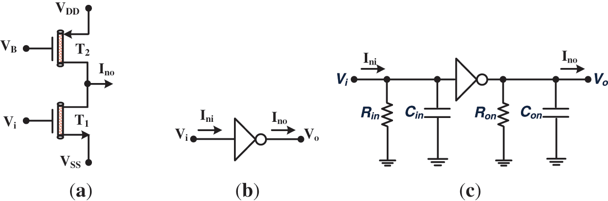
Figure 1: The NT (a) CNTFET realization (b) symbol (c) parasitic model
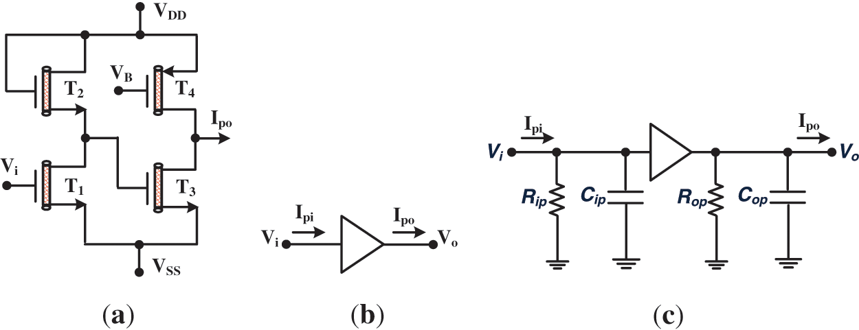
Figure 2: The PT (a) CNTFET realization (b) symbol (c) parasitic model
Here, gm is the transconductance of the PT and NT ABBs. The CMOS based ASP circuit design is based on MOSFETs aspect ratio, while the CNTFET based circuit design is optimized with pitch (SCNT), number of CNTs (NCNT), and diameter (DCNT) [10,29]. The width (W) of CNTFET is given as:
The CNTFET DCNT and threshold-voltage (Vth) are given as [29]:
where, a is graphene lattice constant and (m, n) are chirality vector indices [26]. In this work, the Stanford CNTFET model is used for the circuit verification [31]. This model accurately predicts the transient and AC performance with more than 90% of accuracy and take care of numerous non idealities like effect of drain-source extension region, charge-screening-effect, inter-CNT interconnect wiring capacitance, finite scattering mean free path, drain to source series resistance and many more [10,26].
The proposed FDFAPF topology is shown in Fig. 3. The realized circuit utilizes NTs and PTs as an ABB. The circuit is based on two PTs, two NTs, two grounded resistors and one grounded capacitor. Ignoring the parasitics of employed NTs and PTs, and by considering gm1 = gm2 = gm3 = gm4 = gm, the routine analysis of the Fig. 3, yields the following voltage transfer-function.
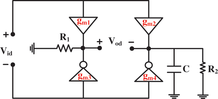
Figure 3: Proposed FDFAPF circuit
If gm*R1 = 1 and R2 = 2R1, an FDFAPF will be realized, with the voltage transfer-function:
From Eq. (7), the pole/zero frequency and phase angle of the FDFAPF can be written as:
The incremental sensitivity of the realized FDFAPF pole frequency with respect to the passive components R2 and C can be obtained as:
From Eq. (10), it is evident that the sensitivity of the pole frequency of FDFAPF with respect to passive component C and R2 are unity in magnitude.
The AO-FDFAPF topology is shown in Fig. 4. This topology is derived from Fig. 3, where resistance R1 and R2 are replaced by negative feedback NTs ABB and capacitance C by a CNTFET varactor. The CNTFET based varactor utilized by AO-FDFAPF is given in Fig. 5. Ignoring the parasitics of employed NTs and PTs, and by considering gm1 = gm2 = gm3 = gm4 = gm5 = gm and gm6 = gm/2, the transfer-function of the AO-FDFAPF can be determined as:

Figure 4: Proposed AO-FDFAPF circuit

Figure 5: Realized varactor using CNTFET
From Eq. (11), the pole/zero frequency and phase angle of the AO-FDFAPF can be written as:
From Eqs. (12) and (13) it is evident that the pole/zero frequency and phase of AO-FDFAPF are dependent on varactor capacitance (C). Thus, the tunability of phase angle can be achieved through control voltage (VC) of the varactor.
The Eq. (11) is obtained under the ideal-conditions and do not consider the influence of NT and PT ABBs input and output ports parasitics. Fig. 6 demonstrates the non ideal equivalent circuit of realized AO-FDFAPF. The overall parasitics at each individual node due to non ideal behavior of NTs and PTs are shown in Fig. 6.

Figure 6: AO-FDFAPF with parasitics
The impact of these non-idealities on the proposed circuit voltage transfer-function is given by following expression.
where,
It is evident from [29], that the parasitic capacitance associated with NT and PT ABBs are in order of aF and also parasitic conductance are in the order of nS. As
To verify the behavior of proposed FDFAPF and AO-FDFAPF, the HSPICE simulations have been performed with 0.7 V supply voltage. The Stanford model with CNTFET parameters (Lg = 16 nm, Ls = 16 nm, Ld = 16 nm, n = 19, m = 0, Vfbn = 0, Tox = 3 nm, Kox = 25, Leff = 15 nm, Lceff = 200 nm, Ksub = 4 SCNT = 10 nm and Efo = 0.6 eV) has been used for verification [26]. Fig. 7 demonstrate the NT and PT frequency response of transconductance with different number of tubes (NCNT). It is noticed that the PT and NT provide almost constant transconductance over 100 GHz frequency range. This constant value of transconductance over a wide range of frequency makes the PT and NT as a good candidate for high frequency applications. It is also observed, that with increasing NCNTs, the transconductance of NT and PT ABBs increases [29].

Figure 7: NT and PT transconductance (gm) frequency response with different NCNTs
The FDFAPF circuit of Fig. 3 is designed to meet the requirement of Eq. (6) to realize the all-pass response at pole frequency fo = 10.9 GHz, with NCNT = 4 for all CNTFETs of the NTs and PTs. This results C = 2 fF, R1 = 3.63 KΩ and R2 = 7.26 KΩ. The Figs. 8 and 9 demonstrate the ideal and simulated gain and phase frequency responses at a design pole frequency of 10.9 GHz, where it is observed that the simulated results, almost matched with the theoretical predictions. The observed transient behavior of the FDFAPF at designed pole frequency is given in Fig. 10, which clearly demonstrates a phase shift of 90o between differential input and output. The observed power dissipation in the designed FDFAPF is 0.66 mW. The Fig. 11 represents the input and output noise simulation results which are found as 22.461 nV/√Hz and 22.257 nV/√Hz respectively, at the designed frequency of 10.9 GHz, which are of insignificant magnitudes. Monte Carlo (MC) analysis of FDFAPF with 30 runs for AC and transient responses are also carried out to investigate the impact of process variations. Figs. 12 to 14 show the outcomes of the FDFAPF MC analysis for gain, phase and transient responses respectively, from which it is evident that there are no significant variations on the FDFAPF performance.

Figure 8: Ideal and simulated frequency response of voltage gain of FDFAPF

Figure 9: Ideal and simulated frequency response of phase of FDFAPF

Figure 10: Transient response of FDFAPF at fo=10.9 GHz

Figure 11: Frequency response of input output noise of FDFAPF
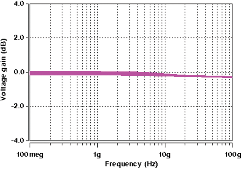
Figure 12: MC simulations of FDFAPF gain

Figure 13: MC Simulations of FDFAPF phase

Figure 14: MC Simulations of FDFAPF transient
Fig. 15 shows the capacitance-voltage simulation results of N-Type CNTFET varactor of Fig. 5, which is utilized in the design of AO-FDFAPF. It is realized with NCNT = 229. It is seen that by altering the varactor tune voltage (VC) from −0.4 V to −0.2 V, the capacitance (C) changes from 2 fF to 0.24 fF. This wide range of capacitance variation by controlling VC, is the key to wide tunability feature of the realized AO-FDFAPF. The AO-FDFAPF circuit of Fig. 4 was also simulated with [NCNT6 = 2, NCNTi = 4], where NCNT6 are the number of tubes utilized for CNTFETs of transconductor 6 and NCNTi are the number of tubes of CNTFETs utilized by all other transconductors to full-fill the primary requirements (gm1 = gm2 = gm3 = gm4 = gm5 = gm and gm6 = gm/2). Figs. 16 and 17 show the gain and phase frequency response results respectively for the AO-FDFAPF, at different values of control voltage (VC). It is observed from Fig. 17, that by altering the VC from −0.4 V to −0.25 V, the AO-FDFAPF pole frequency changes in the range of 10.5 to 26 GHz.

Figure 15: CV characteristics of varactor with NCNT = 229
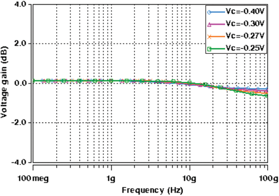
Figure 16: Frequency response of AO-FDFAPF gain at different values of VC

Figure 17: Frequency response of AO-FDFAPF gain at different values of VC
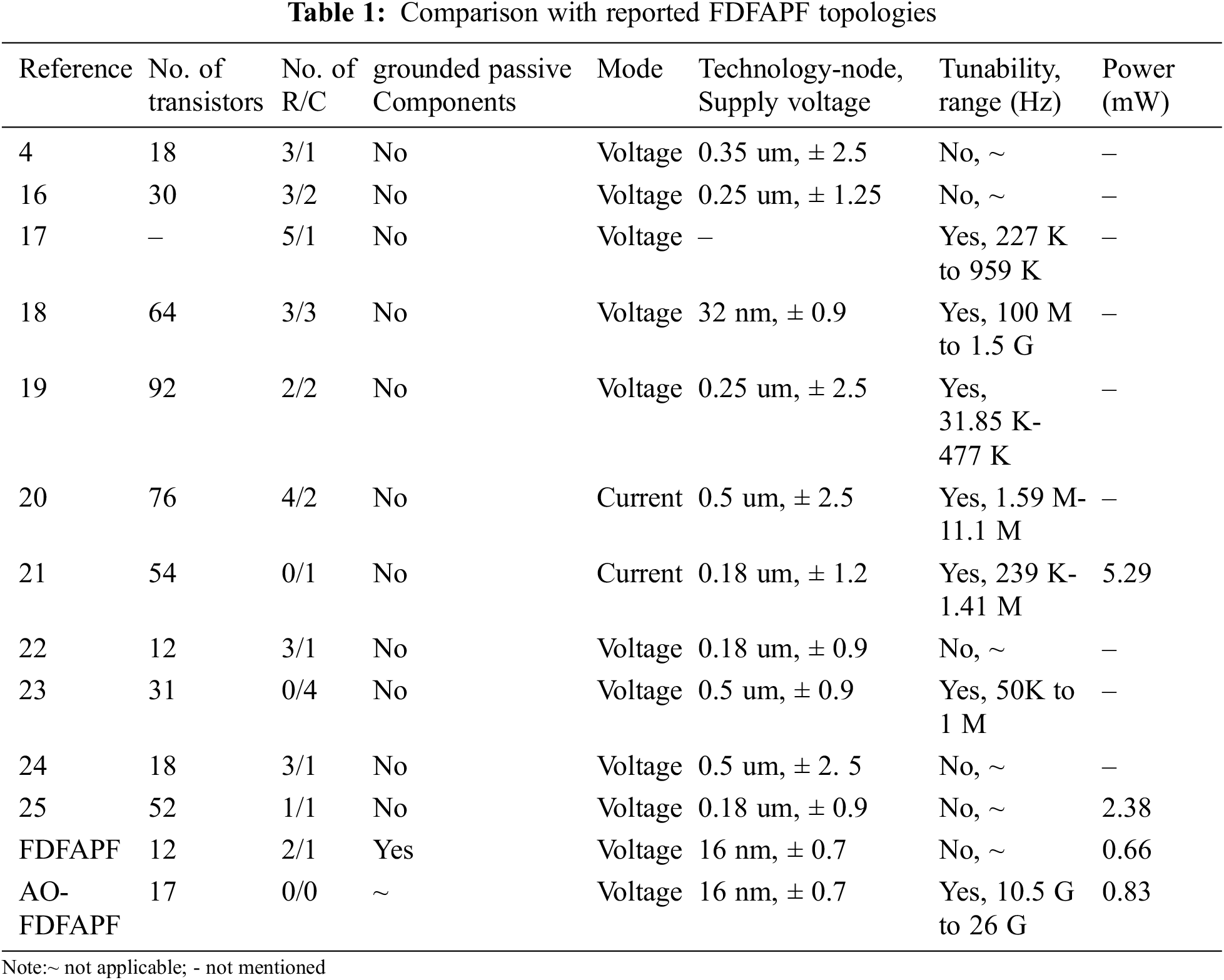
The Tab. 1 demonstrates comparison of the proposed circuits with some other relevant FDFAPF reported in the open literature till date. It is seen that the FDFAPF of Fig. 3 is compact and utilizes lowest active components count as compared to reported FDFAPFs [16–21,23–26]. The APF of [22] also utilizes twelve transistors, however it uses more passive components. Majority of reported APF [16,17,19–26] have frequency limitations where frequency range is limited to few MHz only. The APF of [18] works in the GHz range, however it is based on large number of active and passive components. The AO-FDFAPF of Fig. 4 which is derived from proposed FDFAPF of Fig. 3, does not use any external passive component and thus appropriate for integration. Both the reported filters consume less power as compared to other reported FDFAPFs. It is also to be noted that APF of [16,22,24] are not tunable, however the proposed AO-FDFAPF is tunable for wide band of frequencies.
In this paper, two novel CNTFET based voltage mode fully differential first order all pass filters are presented. Both the proposed topologies utilize CNTFET based compact negative and positive transconductors. The first topology utilizes few transistors and grounded passive components. The second topology is active only fully differential all pass filter derived from the first topology. The tunability of the active only filter is achieved through a single CNTFET based varactor. The ideal and non ideal circuit performance are investigated for the realized filter. Both the filter circuits are simulated with HSPICE by utilizing well known Stanford CNTFET model. The simulation outcomes demonstrate excellent gain, phase and transient characteristics for proposed circuits at high frequencies. The active only filter circuit, demonstrates a wide tunable pole frequency. Moreover, both the filter topologies work equally well on low voltages and dissipate considerable low power. Thus, the proposed filters are ideal candidates for low voltage, low power and high frequency fully differential applications. The simulation outcomes on the proposed filter circuits verify the theoretical predications.
Funding Statement: The authors would like to thank the Deanship of Scientific Research at Umm Al-Qura University for supporting this work by Grant Code: (22UQU4320299DSR01).
Conflicts of Interest: The authors declare that they have no conflicts of interest to report regarding the present study.
1. J. Jerabek, J. Dvorak, R. Sotner, N. Herencsar and J. Koton, “Experimental verification of pseudo-differential electronically controllable multifunction filter using modified current differencing/summing units,” Journal of Circuits, Systems and Computers, vol. 28, no. 6, pp. 1950098, 2019. [Google Scholar]
2. J. Jerabek, R. Sotner, J. Koton, N. Herencsar and K. Vrba, “Pseudo-differential electronically controllable second-order band-pass filter using modified current differencing/summing units,” in Proc. of 40th Int. Conf. on Telecommunications and Signal Processing (TSP), Barcelona, Spain, pp. 320–324, 2017. [Google Scholar]
3. J. Koton, N. Herencsar, O. Sladok and J.-W. Horng, “Pseudo-differential second-order band-reject filter using current conveyors,” AEU-International Journal of Electronics and Communications, vol. 70, no. 6, pp. 814–821, 2016. [Google Scholar]
4. S. Minaei, I. C. Goknar and O. Cicekoglu, “A new differential configuration suitable for realization of high CMRR, all-pass/notch filters,” Electrical Engineering, vol. 88, no. 4, pp. 317–326, 2006. [Google Scholar]
5. S. A. Mahmoud, “New fully-differential CMOS second-generation current conveyer,” Electronics and Telecommunications Research Institute (ETRI) Journal, vol. 28, no. 4, pp. 495–501, 2006. [Google Scholar]
6. J. Koton, N. Herencsar and J.-W. Horng, “Differential second-order voltage-mode all-pass filter using current conveyors,” Elektronika ir Elektrotechnika, vol. 22, no. 5, pp. 52–57, 2016. [Google Scholar]
7. P. Beg, S. Maheshwari and M. A. Siddiqi, “Digitally controlled fully differential voltage-and transadmittance-mode biquadratic filter,” IET Circuits, Devices & Systems, vol. 7, no. 4, pp. 193–203, 2013. [Google Scholar]
8. P. Beg, I. A. Khan, S. Maheshwari and M. A. Siddiqi, “Digitally programmable fully differential filter,” Radioengineering, vol. 20, no. 4, pp. 917–925, 2011. [Google Scholar]
9. S. A. Mahmoud, M. A. Hashiesh and A. M. Soliman, “Low-voltage digitally controlled fully differential current conveyor,” IEEE Transactions on Circuits and Systems I: Regular Papers, vol. 52, no. 10, pp. 2055–2064, 2005. [Google Scholar]
10. M. Masud, A. A’ain, I. Khan and N. Husin, “Design of voltage mode electronically tunable first order all pass filter in ±0.7 V 16 nm CNFET technology,” Electronics, vol. 8, no. 1, pp. 1–19, 2019. [Google Scholar]
11. J. Chhabra, J. Mohan and B. Chaturvedi, “All-pass frequency selective structures: Application for analog domain,” Journal of Circuits, Systems and Computers, vol. 30, no. 8, pp. 1–23, 2021. [Google Scholar]
12. M. Faseehuddin, J. Sampe, S. Shireen and S. H. M. Ali, “Minimum component all pass filters using a new versatile active element,” Journal of Circuits, Systems and Computers, vol. 29, no. 5, pp. 1–31, 2020. [Google Scholar]
13. J. Mohan, B. Chaturvedi and A. Kumar, “New CMOS realizable all-pass frequency selective structures,” Journal of Circuits, Systems and Computers, vol. 30, no. 15, pp. 2150268, 2021. [Google Scholar]
14. N. Herencsar, J. koton, A. Lahiri, U. E. Ayten and M. Sagbas, “Resistorless current-mode first-order all-pass filter with electronic tuning employing low-voltage CBTA and grounded capacitor,” Journal of Circuits, Systems and Computers, vol. 27, no. 2, pp. 1–21, 2018. [Google Scholar]
15. M. Konal and F. Kacar, “DTMOS based low-voltage low-power all-pass filter,” Analog Integrated Circuits and Signal Processing, vol. 108, no. 1, pp. 173–179, 2021. [Google Scholar]
16. P. Beg and M. S. Ansari, “Fully-differential first-order all-pass filters using CMOS DV-DXCCII,” in Proc. of Int. Conf. on Multimedia, Signal Processing and Communication Technologies (IMPACT), Aligarh, India, pp. 267–270, 2017. [Google Scholar]
17. R. Sotner, N. Herencsar, J. Jerabek, A. Kartci, J. Koton et al., “Pseudo-differential filter design using novel adjustable floating inductance simulator with electronically controllable current conveyors,” Elektronika ir Elektrotechnika, vol. 23, no. 2, pp. 31–35, 2017. [Google Scholar]
18. M. I. Masud, A. K. B. A’ain and I. A. Khan, “Reconfigurable CNTFET based fully differential first order multifunctional filter,” in Proc. of Int. Conf. on Multimedia, Signal Processing and Communication Technologies (IMPACT), Aligarh, India, pp. 55–59, 2017. [Google Scholar]
19. I. A. Khan, M. I. Masud and S. I. Moiz, “Reconfigurable fully differential first order all pass filter using digitally controlled CMOS DVCC,” in Proc. of 8th IEEE GCC Conf. & Exhibition (IEEEGCC), Muscat, Oman, pp. 1–5, 2015. [Google Scholar]
20. M. S. Ansari and G. S. Soni, “Digitally-programmable fully-differential current-mode first-order LP, HP and AP filter sections,” in Proc. of Int. Conf. on Signal Propagation and Computer Technology (ICSPCT), Ajmer, India, pp. 524–528, 2014. [Google Scholar]
21. N. Herencsar, J. Jerabek, J. Koton, K. Vrba, S. Minaei et al., “Pole frequency and pass-band gain tunable novel fully-differential current-mode all-pass filter,” in Proc. of Int. Symp. on Circuits and Systems (ISCAS), Lisbon, Portugal, pp. 2668–2674, 2015. [Google Scholar]
22. J.-W. Horng, C.-M. Wu and N. Herencsar, “Fully differential first-order allpass filters using a DDCC,” Indian Journal of Engineering & Materials Sciences, vol. 21, pp. 345–350, 2014. [Google Scholar]
23. L. Acosta, J. Ramirez-Angulo, A. J. Lopez-Martin and R. G. Carvajal, “Low-voltage first-order fully differential CMOS all-pass filter with programmable pole-zero,” Electronics letters, vol. 45, no. 8, pp. 385–386, 2009. [Google Scholar]
24. M. A. Ibrahim, S. Minaei and H. Kuntman, “DVCC based differential-mode all-pass and notch filters with high CMRR,” International Journal of Electronics, vol. 93, no. 4, pp. 231–240, 2006. [Google Scholar]
25. N. Herencsar, R. Sotner, A. Kartci and K. Vrba, “A novel pseudo-differential integer/fractional-order voltage-mode all-pass filter,” in Proc. of IEEE Int. Symp. on Circuits and Systems (ISCAS), Florence, Italy, pp. 1–5, 2018. [Google Scholar]
26. M. I. Masud, A. K. A’ain, I. A. Khan and N. Shaikh-Husin, “A CNTFET-C first order all pass filter,” Analog Integrated Circuits and Signal Processing, vol. 100, no. 2, pp. 257–268, 2019. [Google Scholar]
27. S. Jogad, H. I. Alkhammash, N. Afzal and S. A. Loan, “CNTFET-based active grounded inductor using positive and negative current conveyors and applications,” International Journal of Numerical Modelling: Electronic Networks, Devices and Fields, vol. 34, no. 5, pp. 1–22, 2021. [Google Scholar]
28. S. Jogad, S. Loan, N. Afzal and A. G. Alharbi, “CNTFET based class AB current conveyor II: Design, analysis and waveform generator applications,” International Journal of Numerical Modelling: Electronic Networks, Devices and Fields, vol. 34, no. 1, pp. 1–15, 2021. [Google Scholar]
29. M. I. Masud, A. K. A’ain, I. A. Khan and N. Shaikh-Husin, “CNTFET based voltage mode MISO active only biquadratic filter for multi-GHz frequency applications,” Circuits Systems, and Signal Processing, vol. 40, no. 10, pp. 4721–4740, 2021. [Google Scholar]
30. S. M. A. Zanjani, M. Dousti and M. Dolatshahi, “A CNTFET universal mixed-mode biquad active filter in subthreshold region,” International Journal of RF and Microwave Computer-Aided Engineering, vol. 28, no. 9, pp. 1–9, 2018. [Google Scholar]
31. J. Deng and P. Wong, “A compact SPICE model for carbon-nanotube field-effect transistors including nonidealities and its application—Part II: Full device model and circuit performance benchmarking,” IEEE Transactions on Electron Devices, vol. 54, no. 12, pp. 3195–3205, 2007. [Google Scholar]
 | This work is licensed under a Creative Commons Attribution 4.0 International License, which permits unrestricted use, distribution, and reproduction in any medium, provided the original work is properly cited. |