DOI: 10.32604/EE.2021.014229
ARTICLE
A Novel Polymorphic Topology with Hybrid Control Strategy Based LLC Resonant Converter for Ultra-Wide Input Voltage Range Applications
School of Electrical and Control Engineering, Shaanxi University of Science and Technology, Xi’an, 710021, China
*Corresponding Author: Yong Shi. Email: shiyong@sust.edu.cn
Received: 10 September 2020; Accepted: 05 November 2020
Abstract: To realize effective utilization of renewable energy sources, a novel polymorphic topology with hybrid control strategy based LLC resonant converter was analyzed and designed in this paper. By combining the merits of a full bridge LLC resonant converter, three-level half bridge LLC resonant converter, and variable frequency control mode, the converter realizes an intelligent estimation of input voltage by automatically changing its internal circuit topology. Under this control strategy, different input voltages determine different operation modes. This is achieved in full bridge LLC mode when the input voltage is low. If the input voltage rises to a certain level, it operates in three-level half bridge LLC mode. These switches are digital and entirely carried out by the DSP (Digital Signal Processor), which means that an auxiliary circuit is unnecessary, where a simple strategy of software modification can be utilized. Experimental results of a 500W prototype with 100V~600V input voltage and full load efficiency of up to 92% are developed to verify feasibility and practicability. This type of converter is suitable for applications with an ultra-wide input voltage range, such as wind turbines, photovoltaic generators, bioenergy, and other renewable energy sources.
Keywords: Renewable energy sources; power converter; ultra-wide input voltage range; multi-levels operation mode; hybrid control strategy; soft switching
With the further developments in society and the economy, energy demand is dramatically increasing, and non-renewable energy sources, such as fossil energy, are becoming increasingly exhausted. The energy crisis is getting worse. More scholars are paying attention to new energy technologies, such as photovoltaic generators and fuel cells, and renewable energy sources have become widely used in recent years [1–4]. Compared with traditional energy, the development and utilization of renewable energy is useful measures in solving the energy crisis and environmental pollution. However, due to the influence of natural factors such as climatic conditions, many renewable energy generation units’ power characteristics show discontinuity, poor stability, low utilization rate, and a wide output voltage range. Therefore, it is necessary to design an energy converter that can work in a wide input range in order to realize the efficient utilization of renewable energy sources.
In Fig. 1, zero-voltage switching (ZVS) topologies are preferable for the isolated second stage to enhance efficiency. In particular, the multi resonance LLC topology has several advantages over ZVS topologies. These advantages include:
a) Primary side switches can realize zero -voltage switching (ZVS) in the full load range.
b) Secondary rectifying diodes can realize zero- current switching (ZCS), thus reducing the switching loss.
c) Only the capacitor is applied as the output filter compared with the traditional LC filter.
d) Since there is no filtering inductance on the secondary side of the converter, the voltage stress of the full bridge rectifier diode is only the output voltage.
e) Simple structure due to the absence of clamp circuit.
f) Low EMI radiation.
LLC resonant converters can realize high efficiency, high power density, and low cost of power conversion, which have been analyzed and studied as the topology of this paper [5–9].
The LLC resonant converter has become a hot research topic in the past two decades. Generally speaking, the LLC resonant converter operates through a variable-frequency (VF) control strategy, and its operating frequency range is limited. Therefore, it is not suitable for applications with a wide input voltage range. To solve this problem, some scholars have proposed various improvement methods for LLC resonant converters based on a new topology and control strategy.
In [10], a multilevel working mode half bridge LLC resonant converter has been proposed, which can operate in two-level modes according to the input voltage. However, there is not a smooth transition between the two modes. Besides, the selection of transformer ratio, series resonant capacitance, leakage inductance, and other parameters lack sufficient theoretical bases.
A full bridge three-level LLC resonant converter is presented in Reference [11]. Although this converter operates in both three-level and two-level modes, as well as a wide input voltage range with a constant switching frequency control strategy, not all switches have a voltage stress half of the input voltage in three-level mode. Besides, both modes are difficult to control.
In [12], an LLC resonant converter with two series transformers was proposed, and its input voltage range can reach a maximum and minimum input voltage ratio of six. However, the parametric design process can be quite complicated.
Summarizing the existing literature on LLC resonant converter with a wide input voltage range, we have found that there is a lack of a relatively simple and accurate design method. This paper’s main contribution is to propose a novel polymorphic topology with hybrid control strategy-based LLC resonant converter for ultra-wide input voltage range applications. The converter integrates two different high efficiency DC-DC converters to solve high pressure stress and low conversion efficiency. For the polymorphic converter, the internal circuit structure can be automatically changed. It is suitable for maximum efficiency of the two independent input voltage ranges of 100V~300V and 300V~600V. To save costs, the total number of power components (active and passive) of the two converters remains the same, sharing the same resonant cavity and high frequency transformer. When the circuit topology changes, the voltage stress of each switch will be half of the input voltage, and the advantages of soft switching remain unchanged. In this paper, the specific working principle and design idea are detailed. A 500W prototype with an input voltage range of 100V~600V and an output voltage of 48V have been built, which verifies the validity and applicability of the converter.
2 Principle and Working State Analysis of Polymorphic Topology
A novel polymorphic topology converter, which integrates two DC-DC topological structures, has been realized by a series of interface circuits composed of MOSFET as switches and DSP (Digital Signal Processor). With different input voltages, the converter’s circuit structure changes by controlling the on and off of the MOSFET. As shown in Fig. 1, the topological structures and working mode of the two DC-DC converters are determined by the switches. When  ,
,  are off, and
  is on, a three-level half bridge LLC resonant converter suitable for input voltages of 300~600V is available; when
  ,
,  are on, and
  is off, a full bridge LLC resonant converter with input voltage 100V~300V is built. In Fig. 1, the three MOSFETs
  ,
,  , and
, and  are switches,
  and
and  are input filter capacitors, the four MOSFETs
  ~
~ are main power switches while
 ~
~ and
and  ~
~ are their parasitic diodes and capacitors, respectively. The primary side resonance inductance
  (including the primary side leakage inductance of transformer), the resonant capacitance
 , and the excitation inductance
  constitute the resonant cavity. Since the resonant capacitor is in series on the primary side circuit, it also plays a role of isolation. The transformer excitation inductance enables the parallel connection between
  and the transformer.
  is the ratio of primary and secondary side turns of transformer
  . The ultra-fast recovery diodes
  ~
~ of the secondary side constitute a full bridge rectifier circuit.
  is the output filter capacitor, and
  is the load resistance.
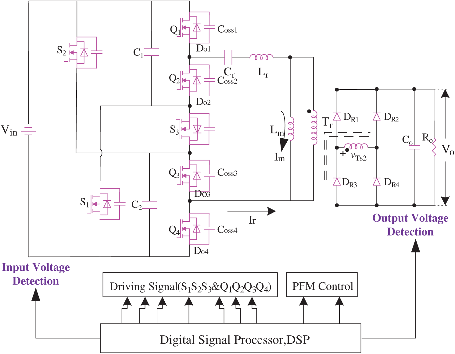
Figure 1: Polymorphic topology converter
PFM (Pulse Frequency modulation) has been adopted in both two working modes. The ePWM1A, ePWM1B, ePWM2A, and ePWM2B of DSP output the drive signals with fixed duty cycle and dead zone time. The main power switches  ,
,  ,
,  , and
, and  are driven by the control circuit for energy conversion. The working principles of the two modes are listed as follows:
2.1 300V~600V High Line Input (Three-Level Half Bridge LLC, Mode1)
When the input voltage is high, a novel ZVZCS three-level half bridge LLC resonant converter is used on the primary side, as given in Fig. 2, which turns on  while
while  and
and  is off. Two input divider equalization capacitors
  and
and  in series are connected in parallel with the input voltage
  , providing a midpoint potential to clamp the switches so the voltage stress is
  and facilitating the realization of soft switching. The four main power switches
  ,
,  ,
,  , and
, and  are connected in series to form a three-level half bridge structure. In appearance, it is similar to the conventional three-level half bridge DC-DC converter. Nevertheless, its driving signal pulse modulation mode of the main switch is different, which results in a substantially different working principle and performance from the conventional three-level circuit. The driving signals of the four primary switches and the three switches are in Fig. 3.
  and
and  are of the same set of driving signals;
  and
and  are also of the same set. The driving signals of
  and
and  are complementary, so are
  and
and  , and their duty cycle is 50% (regardless of dead-time). The output voltage is controlled by changing the switching frequency, which means the PFM modulation is applied instead of the traditional PWM modulation. Before the analyzing, we have made the following assumptions:
a) The capacity of two input capacitors in series is infinite, replaced by two 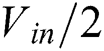 voltage source.
b) All power switches and diodes are ideal devices.
c) All capacitors, inductors, and transformers are ideal devices.
d) Output capacitance  is considered to be infinite and is replaced by the constant voltage source
  .
.
e) The circuit has been working in a stable state.
The switching cycle of the converter can be divided into eight stages. The main work waveform, as shown in Fig. 3, shows that the waveforms of the first half of the cycle and the second half are symmetrical. Therefore, only half of the cycle (five of the eight stages) is analyzed below, corresponding to the five equivalent circuits shown in Fig. 4. The working processes are described as follows:
Figure 2: ZVZCS TLHFLLC power architecture
Figure 3: Key waveforms of the ZVZCS TLHFLLC
Stage 1 [Fig. 4a, before  ]: Before
  ,
,  and
and  turn on. At the same time,
  and
and  are turned off. The resonant inductance current
  is positive and flows through
  and
and  . The excitation inductive current
  linearly increase due to the input partial voltage capacitance
  and
and  ,
,  . Meanwhile, the secondary diodes
  and
and  will turn off automatically due to the zero-crossing current. So, there will be almost no reverse process. This working state of the diode is defined as the zero-current switching (ZCS). The voltage spike on the diode operating in the ZCS state is almost zero.
  ,
,  , and
, and  resonate together.
Stage 2 [Fig. 4b,  –
– ]: Turn off
  and
and  at
at  . At this point, the resonant current
  charges
  and
and  and discharges
  and
and  .
.  and
and  shut off with zero voltage due to the buffering of
  and
and  . The resonant current
  rises with the sine wave, and then decreases after reaching its peak, and the excitation current
  linearly increases at the same time. When the resonant current
  and excitation current
  are equal, the voltages at both ends of the excitation inductance
  are no longer clamped by the output voltage
  . The resonant capacitor
  , resonant inductance
  , and excitation inductor
  participate in the resonance, and the three-element resonance occurs. Since the excitation inductance
  is much larger than the resonant inductance
  , the current variation in this segment is relatively smooth, and the resonant current
  can be regarded as a constant value. In this state, the output capacitance
  continues to provide energy for the load
  . The equations of
  ,
,  , and
, and  are as follows:


where  is the peak value of excitation inductance current, and
  is the initial value of resonant capacitor
  at
at  .
.
Stage 3 [Fig. 4c,  –
– ]: At
]: At  , the voltage of parasitic capacitance
  and
and  of
of  and
and  rises to
  , and the voltage of parasitic capacitance
  and
and  of
of  and
and  drops to 0, At this time,
  and
and  can be turned on with zero voltage. Since this period is short, we can approximate that both
  and
and  remain unchanged. There is no current in the primary and secondary sides of the transformer, and the load
  is still powered by the output capacitor
  . The parasitic capacitance of
  and
and  begins to discharge until its voltage becomes 0.
Stage 4 [Fig. 4d,  –
– ]: From
  , the resonance current
  and excitation current
  begin to decline, and
  and
and  start to become unequal. When the rectifier diodes
  and
and  are conducting, as indicated by Kirchhoff’s current law, the secondary diode current
  flows forward from zero. The voltage on the secondary side of the transformer is clamped by output voltage
  , and the voltage at both ends of the excitation inductance
  is clamped to
  by output voltage
  . At this time, only the resonant capacitor
  and resonant inductor
  participate in the resonant cavity, when three-element resonance becomes two-element resonance. The equations of
  ,
,  , and
, and  are as follows:


where  is the transformer primary to secondary turn ratio,
 ,
, .
.
Stage 5 [Fig. 4e,  –
– ]: When the excitation current
  is equal to the resonant current
  at
at  -
- , the secondary rectifying diodes
  and
and  stop conducting, realize zero-current switching (ZCS), and begin to bear the reverse voltage. During this period, resonance current
  decreases to 0 in the positive direction and then increases in the negative direction. Thus, resonance current
  starts to charge the excitation inductance
  again, and the excitation current
  linearly increases (negative).
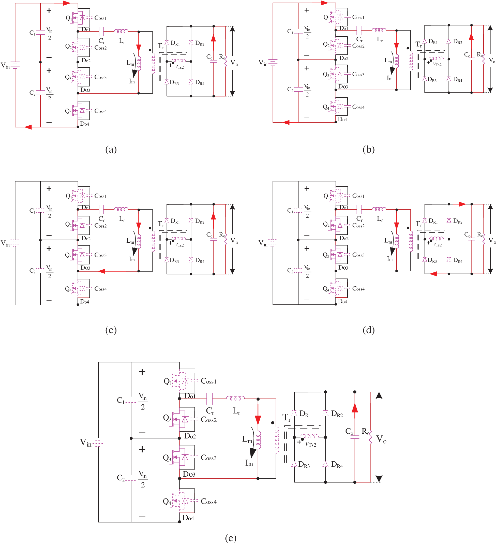
Figure 4: Equivalent circuits for different time intervals in half of the switching cycle: (a) Stage 1; (b) Stage 2; (c) Stage 3; (d) Stage 4; (e) Stage 5
After  , the first half cycle of the converter’s working state ends, and the second half cycle begins. The working state of the second half cycle is symmetrical with the first half cycle (
 -
- ), and they will not be repeated here.
2.2 100V~300V Low Line Input (Full Bridge LLC, Mode 2)
When the input voltage is low, the traditional full bridge LLC resonant converter is in work, which operates by turning on  ~
~ and turning off
  . Due to the use of three-level technology, the maximum voltage of the primary side MOSFETs is only 300V, so it is unnecessary to change the type and parameters of the primary side switch. In addition, the full bridge LLC resonant converter still adopts the same parameters of the resonant cavity. Therefore, the two circuit topologies within the entire input voltage range work through the same set of circuit components, which saves costs and maximizes economic returns.
Since the operating principle and design analysis, including the optimum for ZVS parameters, have been well developed and introduced in the literature [13,14], detailed analysis of this converter has omitted for conciseness.
3 Influence of Wide Input Voltage Range on LLC Converter
As the switching frequency  varies closer to the resonant frequency
  under the VF control strategy, the fundamental harmonic approximation (FHA) method is used to obtain the voltage gain characteristics [15–18]. The following is a specific derivation process.
3.1 Limitations of Voltage Gain Characteristics
The resonant network equivalent circuit of the LLC resonant converter is shown in Fig. 5.  is the basic wave of the input voltage, and
  is the equivalent resistance when the load converts to the primary side.
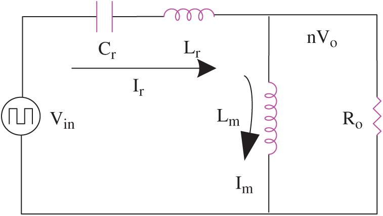
Figure 5: Equivalent circuits for resonant tank
The resonant network is composed of resonant capacitor  , resonant inductor
  and transformer excitation inductor
  , so there are two resonance frequencies
  and
and  as shown in Eqs. (7) and (8).


According to Fig. 5, the LLC resonant converter’s voltage gain function is derived from the fundamental wave analysis method (FHA) as:
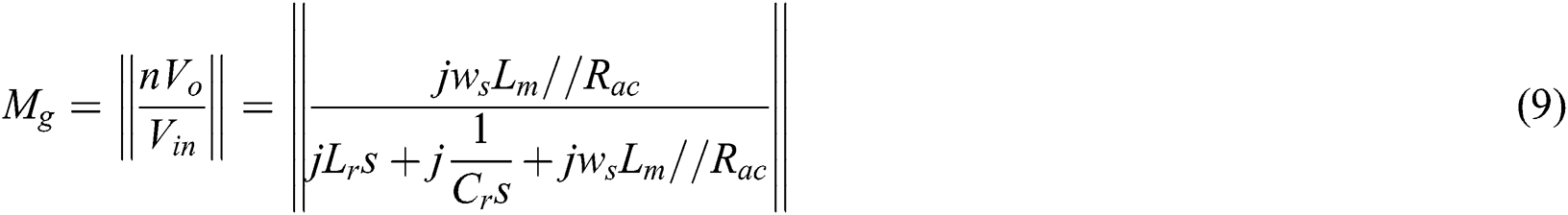
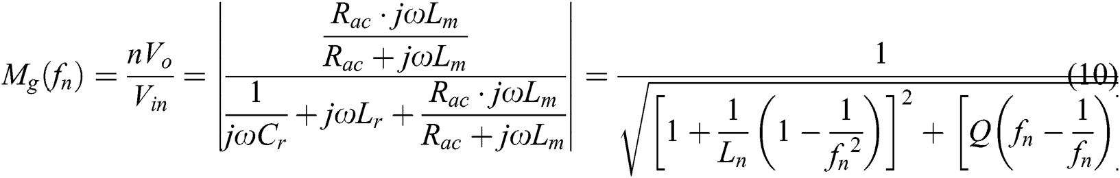
where  is the inductance ratio between magnetizing inductance
  and the resonant inductance
  ,
,  is the normalized frequency ratio between the switching frequency
  and resonant frequency
  ,
,  is the quality factor of resonant tank,
  is the equivalent ac load resistance, and
  is the switch angle frequency.
Input impedance  of the resonance network is as follows:

If the characteristic impedance  is used to normalize, the input impedance
  after normalization can be obtained by:
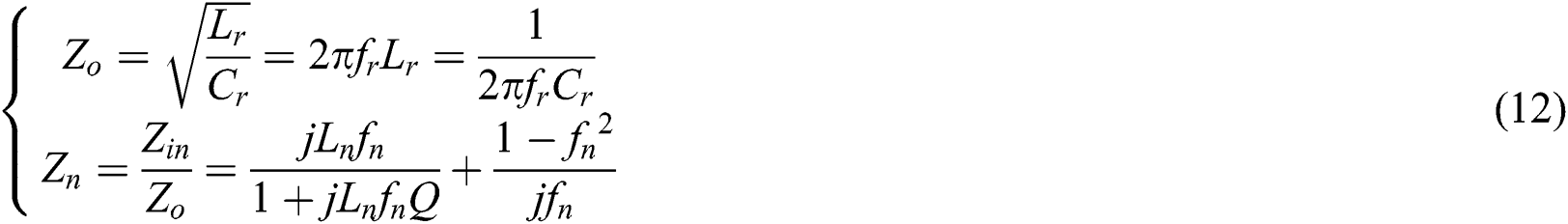
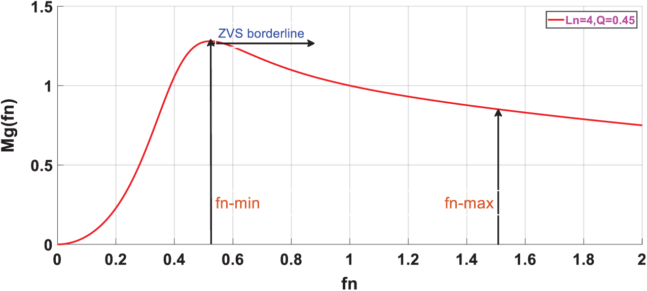
Figure 6: The voltage gain curves of resonant tank under and
and 
It can be concluded from Eq. (10) that the values of each group of  and
and  correspond to different voltage gain curves
  . If we select
  and
and  as a set of specific values, we can obtain a resonant network’s voltage gain curve, as shown in Fig. 6. When the square wave voltage passes through the resonant network, the phase difference will be generated between the current and voltage waveform, enabling the switches to realize zero-voltage switching (ZVS), that is to say, the input impedance presents sensibility. The LLC working area can be divided into two parts according to the opening state of the switches (ZVS and ZCS). The peak point of the gain curve is the boundary point of ZVS and ZCS. If the imaginary part of
  is 0, the perceptual boundary condition of input impedance can be obtained, as shown in “ZVS boundary line” in Fig. 6, the right side of the boundary line is the region where ZVS can be realized. In the ZVS region, the regulation range of switching frequency (
 ) limits the value of the resonant network’s voltage gain, thereby limiting the range of input voltage adaptation. In the design, the maximum voltage gain obtained at the lowest switching frequency shall meet the gain demand at the minimum input voltage; the minimum voltage gain obtained at the highest switching frequency shall meet the gain demand at the maximum input voltage. Besides, within the ZVS region, the slope of the voltage gain curve decreases with increasing
  , which means that the regulating range of switching frequency extends with increased input voltage. A high switching frequency is required to obtain a small enough voltage gain to maintain the output voltage’s stability during the high voltage input. In practice, switching frequency is often limited by switching devices. The over-high frequency will also bring problems such as switching loss, voltage and current waveform oscillation, and electromagnetic interference (EMI), which is another essential factor to limiting the input voltage range.
3.2 Influences of  and
and  on Voltage Gain Characteristics
According to Eq. (10), the resonant network’s voltage gain of the LLC converter is affected by  and
and  , determining the input voltage range of the converter. Therefore, it is necessary to select an appropriate
  and
and  to meet the requirements of the adaption range of the input voltage in the design. Fig. 7 shows the resonant network voltage gain curve with the same
  and different
  . According to this Fig. 7, in the region of
  , the voltage gain increases with decreasing
  . The maximum gain also increases, so that the resonant network can adapt to a smaller input voltage. However, in the region of
  , the voltage gain increases with decreasing
  . The slope of the gain curve becomes smaller, which means that with decreasing
  , the adjustment range of switching frequency becomes larger and larger during the high voltage input. Meanwhile, the minimum voltage gain obtained at the highest switching frequency becomes larger, and the upper limit of the input voltage adaptation range decreases.
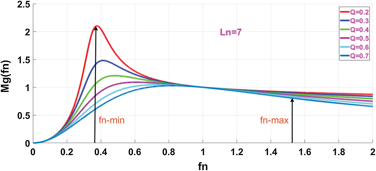
Figure 7: The voltage gain curves of the resonant tank under different 
Fig. 8 shows the voltage gain curve of the resonant network under the same  and different
  . As can be seen from Fig. 8, in the region of
  , voltage gain increases with decreasing
  , and the maximum gain also increases, so that the resonant network can adapt to a smaller input voltage. In the region of
  , the voltage gain decreases with decreasing
  ; the slope of the gain curve increases with the decrease of
  . It shows that with decreasing
  , the frequency adjustment range of the high voltage input becomes smaller, and the minimum voltage gain obtained at the maximum switching frequency becomes smaller, so that the resonant network can adapt to the higher input voltage.
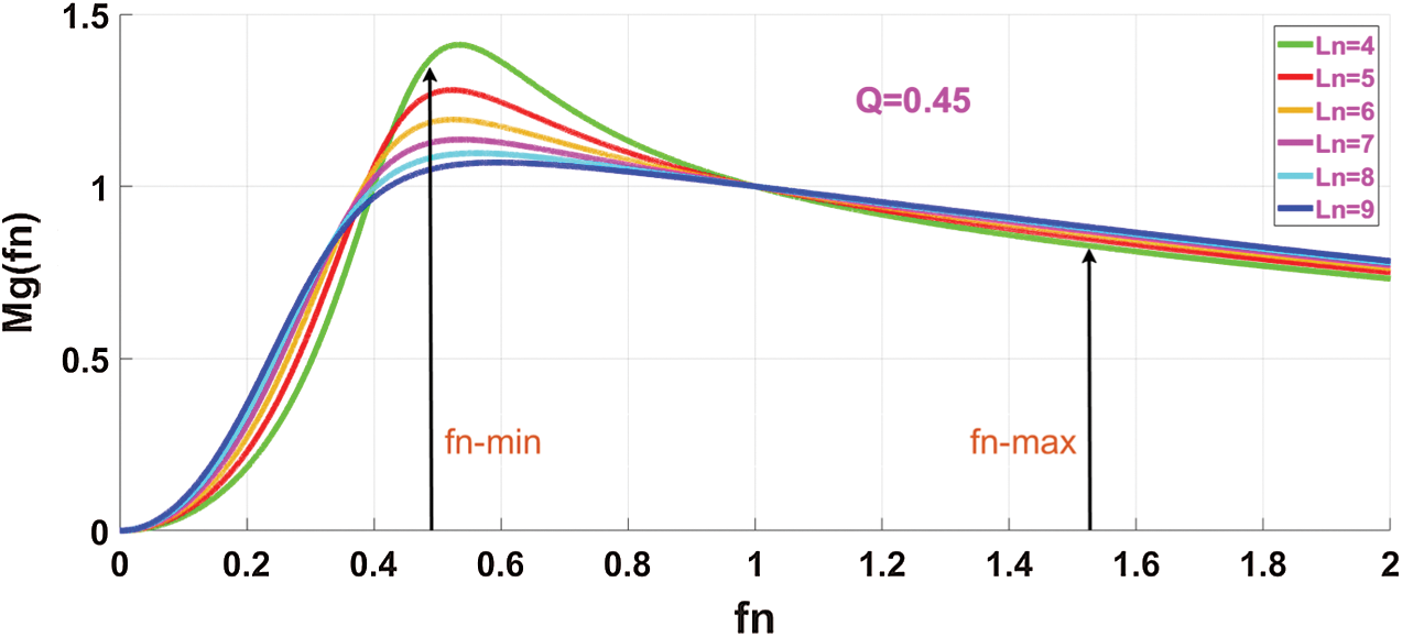
Figure 8: Voltage gain curves of the resonant tank under different 
On the whole, using a small  can only expand the lower limit of the input voltage range, but not the upper limit. So, reducing
  to expand the input voltage range of the LLC converter is not considered. Therefore, it is often used to reduce
  in the design to expand the upper and lower limits of the input voltage range for the LLC converter.
Based on the above theoretical analysis, it is concluded that the adjustment range of resonant frequency ( ) determines the effective range of the resonant network’s voltage gain (
 ). In the design, the maximum voltage gain of the resonant network should meet the requirement of the minimum input voltage of the resonant network, and the minimum voltage gain should meet the requirement of the maximum input voltage. The LLC converter was designed with a small
  to acquire a wide input voltage range while maintaining high efficiency.
4 Parametric Consistency Design for the Polymorphic Topology LLC Resonant Converter
The design of the resonant cavity’s parameters of the LLC resonant converter includes the resonant inductor  , the resonant capacitor
  , and the excitation inductor
  . For the polymorphic topology LLC resonant converter proposed in this paper, it needs to meet the following two requirements: (1) Adaptation to a wide input voltage range; (2) Soft switching realization within the full load range (ZVS at the primary MOSFETs and ZCS at the secondary diodes). The LLC converter’s parameters need to be defined before designing, such as input and output voltage ranges, the maximum output power, and the resonance frequency. Therefore, the input voltage range is 100V~600V, and the nominal value is 300V. The output voltage and maximum output power are 48V and 500W, respectively. In this design, the resonant frequency
  is selected to be 180 kHz. The following are the step-by-step design procedures illustrated in Fig. 9.
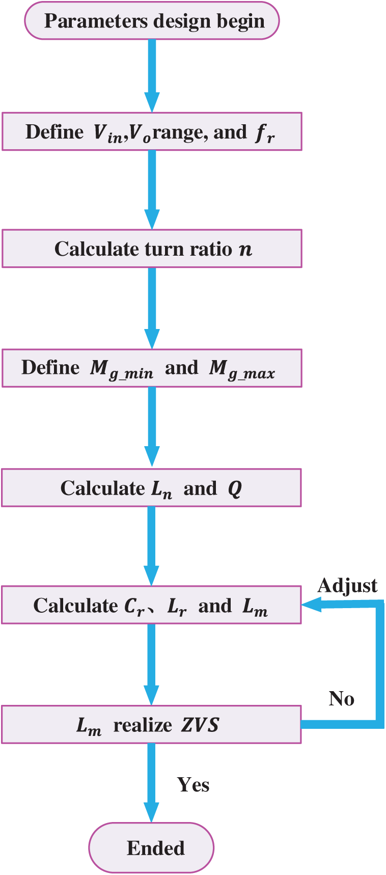
Figure 9: Flow chart of LLC parameter design
Before it is designed, the initial parameters of the LLC resonant converter should be defined, such as the input and output voltage range, the maximum output power, and the maximum resonant frequency. Then, the input voltage of the LLC converter varies from  to
to  , with a nominal value of
  . In this design,
 was chosen.
a) Selecting the Transformer Turns Ratio 
Due to gain of the LLC resonant converter being constant at 1 for  and independent of load, its resonance gain was set to 1, enabling a freer design of resonance parameters and leaving more space for the design of the LLC resonance parameters. Under the premise of realizing soft switching, the switching frequency will be lower, the loss will be less, and the working efficiency will be higher.
The transformer turns ratio should be selected at the resonant frequency, where the gain is unity. It can be calculated as:

where  is the diode voltage drop of the output rectifier.
b) Define Maximal and Minimum Voltage Gain
After the theoretical turn ratio was determined, the maximum and minimum voltage gains were calculated according to the input voltage range to ensure that the output voltage can be adjusted.


c) Calculating  and Q
and Q
The resonant cavity parameter design of the LLC resonant converter includes resonant inductance  , resonant capacitor
  , and excitation inductance
  . The inductance ratio
  and quality factor
  determine the magnitude of them, so the design of the resonant cavity’s parameters is about to select the values of
  and
and  . From previous research regarding voltage gain characteristics under VF mode, the selection of the parameters
  and
and  directly influence the converter’s input voltage range. Therefore, based on the traditional design method of parameters, this paper will present the influence of the critical parameters
  and
and  on the gain curve. Then, combined with an index system for key parametric value restrictions, we will select a reasonable set of parameters, verified by back substitution equations, and constantly optimized, to finally determine
  and
and  . In this design, we have assigned
  ,
, .
.
d) Calculating  ,
,  , and
, and 
The resonant capacitor value is given by:

Once the value of the resonant capacitor is determined, the resonant inductor value and the transformer magnetizing inductor value can be calculated by using Eqs. (17) and (18).


e)  Requirements
To achieve ZVS at  with a duty cycle of 0.5,
 must meet the inequality Eq. (19). If it is not satisfied, the dead time in Eq. (19) should be set again or, the aforementioned design should be tuned.

where  is the equivalent output parasitic capacitor of primary switches, and
  is the dead-time of upper and lower switches.
Based on the above steps, the most reasonable resonant parameter values have been finally obtained. The wide input adaptability of the novel polymorphic topology LLC resonant converter will be verified in the following experiments.
5 Implementation Scheme of Polymorphic Topology Switching Control Strategy
Since the circuit topology of hybrid mode LLC is different under different input voltages, an appropriate topology switching strategy is needed to make the LLC switch between different topologies. Besides, the strategy will prevent the circuit from producing excessive impact oscillation, which will create an unstable system or destroy the circuit. Since the topologies of the three-level half bridge and the full bridge circuit are derived from the full bridge topology, no additional devices are necessary, and the switching between topologies can be realized by using its own MOSFET as the switch, which reduces the cost. In circuit simulation, devices usually start when the input voltage exceeds a certain switch point. However, in practice, due to the ripple or sudden change of input voltage, the switching signal will continuously oscillate. To avoid this situation, we must set a certain difference in the switching voltage. For the polymorphic topology introduced in this chapter, there are two switches in it. The first is the switching between full bridge variable frequency control and full bridge constant frequency control, and the second is the switching between full bridge constant frequency control and half bridge variable frequency control.
This section will introduce the control strategy and solution of the polymorphic topology control circuit shown in Fig. 10, which implements two operating modes of the converter at different input voltage levels to improve the wide range adaptability of the LLC converter.
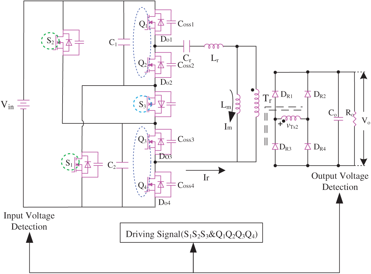
Figure 10: Polymorphic topology control circuit
Usually, polymorphic mode switching circuits rely on switches. Conventional switches are hardware latches and relays. These two kinds of switches have shortcomings: The hardware latch needs an inconvenient manual operation, and the speed of relay switching is too slow to withstand pressure and volume conflict. Besides, the durability of the relay’s contact is inferior, and its maintainability is poor. The polymorphic topology circuit studied in this paper uses MOSFETs of the circuit itself as the switches. It does not need to add an additional auxiliary circuit, reducing the number of components to a minimum while maximizing cost-effectiveness.
In general, once the input voltage exceeds the voltage of the settled switching point, the circuit should be immediately activated. If the circuit is reconfigured, the energy stored in the circuit components will not be released. So, the extreme high dv/dt and di/dt may occur during the switching process. To eliminate this negative impact, we need to develop a more flexible control strategy. The proposed control strategy in this paper adopts the concepts of cutting off power input, outputting energy consumption, and topological switching. For example, when the converter circuit is switched from full bridge LLC to three-level half bridge LLC, the switching process is divided into three stages: 1)  ~
~ and
and  ~
~ are simultaneously turned off to be isolated from the input power; 2) Then wait until the output load consumes up the energy stored in the circuit; 3) Finally, open
  and
and  ~
~ at the same time. The whole switching process will be completed. The entire switching process takes time, but the output capacitance
  is large enough to power the output load
  . In practice, a hysteresis comparison link should be added to the detection of switching point voltage to avoid incorrect switching of the converter’s operation mode caused by detection error.
5.1 Generation of the Drive Signal
For the analog circuit, the generation of switching action of polymorphic topology is quite complicated. The original drive signal must be stopped, and a new drive signal must be generated. In this paper, DSP is adopted for full digital control to sample and monitor the input voltage. When the input voltage is lower than the set value, full bridge LLC topology is adopted; when the input voltage rises to a certain level, the topology switches to a three-level half bridge LLC. The specific generation mode of the drive signal is as follows:
The time-varying sawtooth pulse is generated by the period counter (TBCTR), and the enhanced pulse width modulation module ePWM1 (EPWM1A, EPWM1B) is used to control  and
and  , the ePWM2 (EPWM2A, EPWM2B) is used to control
  and
and  , and the ePWM3 (EPWM3A, EPWM3B) and ePWM4(EPWM4A) are used to control
  ,
,  , and
, and  , respectively.
The whole control process is divided into two parts: When the topology of the converter’s circuit is in the full bridge or three-level half bridge, ePWM1 and ePWM2 generate drive signals as shown in Fig. 11a respectively, and the driving signals of the tube are consistent at this time. When the circuit topology is switching, the drive signal shown in Fig. 11b is implemented to generate permanent on and off signals.
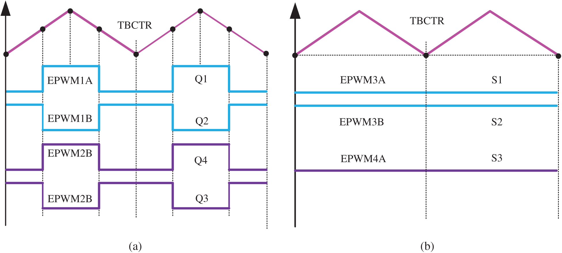
Figure 11: Principles of generating driving signal. (a) Driving signals for  and (b) Driving signals for
5.2 Analysis of Switch State in the Process of Changing Topology
 ,
,  and
and  ,
,  form two pairs of bridge arms, respectively, in the primary circuit of the converter. The bidirectional fluidity of resonant current
  enables two switches to simultaneously conduct for each working state. Suppose “1” and “0” are used to indicate the state of on and off, respectively. In that case, we will acquire the switching state of LLC converter shown in Tab. 1, considering that two switches of the same bridge arm cannot be connected at the same time, so
  ,
,  , and
, and  of different circuit topologies cannot also be concurrently connected.
Table 1: Driving states of the LLC converter
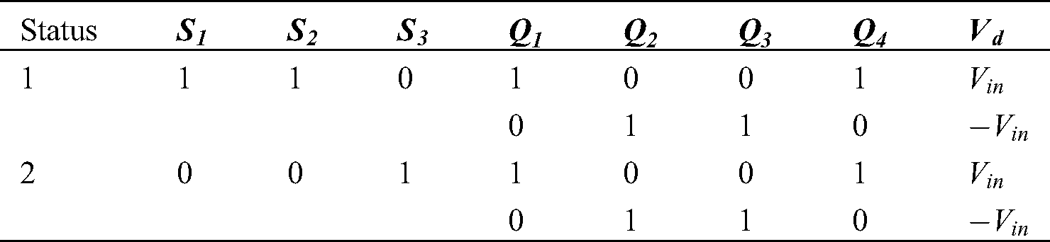
When the switches are driven alternately according to the status 1 in Tab. 1, the circuit topology of the converter is full bridge LLC converter, and there are two kinds of input voltage  and
and  in the resonance network; When the switches are driven in status 2 in Tab. 1, the circuit topology of the converter is a three-level half bridge LLC converter, and there are also two kinds of input voltage
  and
and  in the resonance network. In the two circuit topologies, the resonant network has the same input voltage. The LLC converter works in multi-levels mode, which also conforms to the consistent design requirements of LLC resonant parameters described above. Experimental results show that the topology switching control strategy is practical and straightforward.
6 Hardware Prototype and Experimental Verification
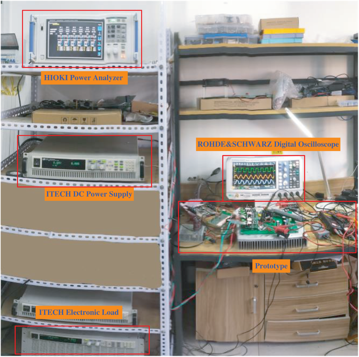
Figure 12: Experimental setup
In this paper, hardware implementation of the prototype was carried out in the laboratory. A photograph of the experimental prototype and setup is shown in Fig. 12. A 500W experimental prototype, suitable for renewable energy sources and with the adoption of the proposed polymorphic topology control strategy for an ultra-wide input voltage range, has been established to verify analysis in this paper. The specification and main parameters used by the experimental prototype are summarized as follows: the input voltage is 100V~600V, the output voltage is 48V, and the maximum output current is 10.5A. The turn ratio of transformer is 18:6, which means the LLC resonant converter works in the stable condition at the ideally input voltage of 300V. The detailed design criteria are listed in Tab. 2.
Table 2: Utilized components and parameters in the prototype
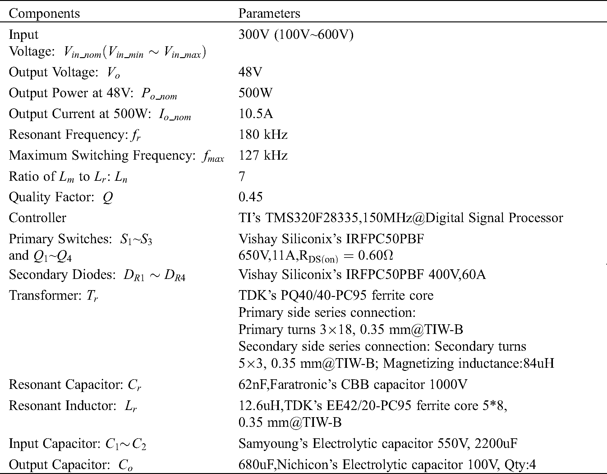
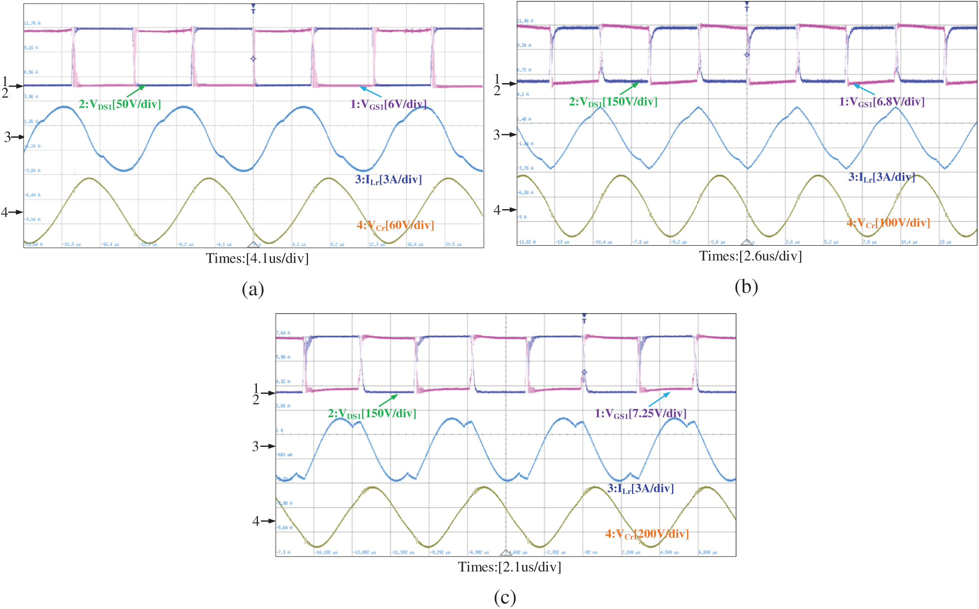
Figure 13: Experimental results with different input voltages: (a) Waveforms under input voltage 100V condition ( [6V/div],
  [50V/div],
  [3A/div],
  [60V/div]); (b) Waveforms under input voltage 300V condition (
 [6.8V/div],
  [150V/div],
  [3A/div],
  [100V/div]); (c) Waveforms under input voltage 600V condition (
 [7.25V/div],
  [150V/div],
  [3A/div],
  [200V/div])
A prototype converter was built and tested in the lab to verify the proposed method. The resonant frequency was chosen to be high to reduce the parasitic effects in the circuit. The experimental waveforms of a proposed converter are shown in Figs. 13a–13c. Most of the results have similarities with simulated and theoretical calculations. Fig. 13 shows the experimental waveforms of the  drive voltage (
 ), the voltage across
  (
( ), resonant tank current (
 ), and resonant capacitor voltage (
 ) at
) at 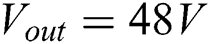 . As shown in Fig. 13a, the switching frequency
  . The waveforms in Fig. 13b are given at
  . Fig. 13c presents the waveforms at the maximum input voltage, while operating at the maximum frequency.
Figure 14: ZVS waveforms of switches  and
and  with the converter at full load: (a)
  , waveforms of
  ; (b)
; (b)  , waveforms of
  ; (c)
; (c)  , waveforms of
  ; (d)
; (d)  , waveforms of
  ; (e)
; (e)  , waveforms of
  ; (f)
; (f)  , waveforms of
It can be seen from Fig. 14 that all primary side MOSFETs can achieve ZVS in the full load. The switches turn on in ZVS condition and turn off at a very low current. Therefore, the high frequency turn-on switching losses become negligible. There are no significant voltage spikes across the switches, which signify the ZVS turn-off transition. The MOSFET becomes switched off completely before the drain to source voltage rises above zero. Due to ZVS, the losses of turn-off transition are reduced to a very small value. It is also seen that the voltage stress of the primary switches is half of the input voltage. This is because the low voltage rated MOSFET with low  is employed to reduce conductivity losses.
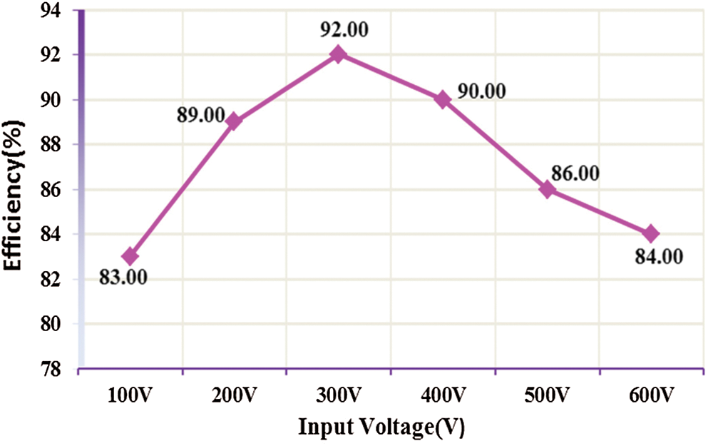
Figure 15: Efficiency curve of the prototype
The efficiency curve of the system with different input voltage is shown in Fig. 15. The experimental result was obtained by HIOKI PW6001, where the full load was 500W. The overall efficiency of the converter is ideal, and peak efficiency can reach 92%.
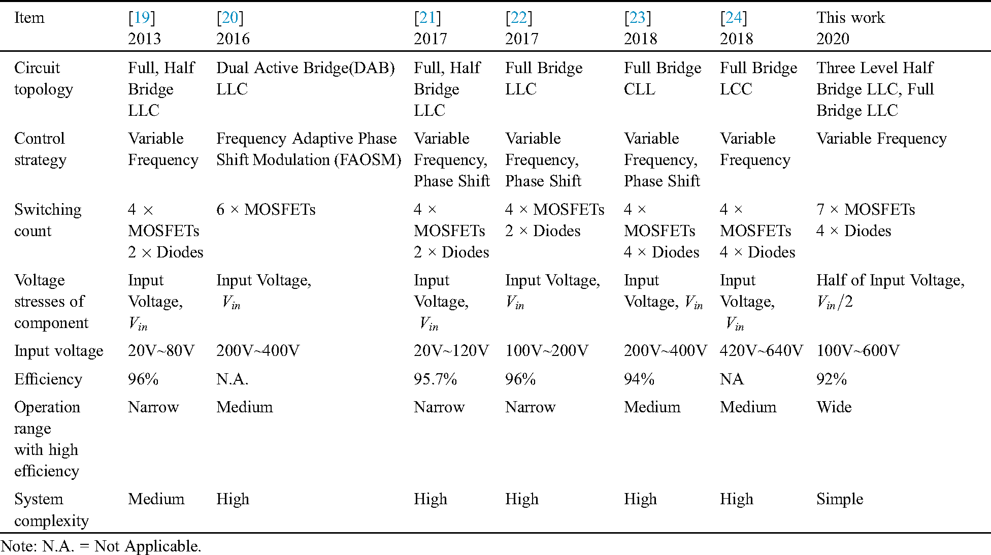
Currently, research literature is often focused on extending the input voltage range with higher efficiency, decreasing components count, and system complexity, and minimizing size, weight, losses, and stresses of component. To evaluate the characteristics of the proposed polymorphic topology, the performances of the proposed method and other different kinds of control techniques in recent years have been compared, as summarized in Tab. 3.
Tab. 3 shows the comparisons with other relevant literatures, while also showing the features and advantages of our work. Hence, through comparison and analysis, the novel polymorphic topology, was shown to be suitable for ultra-wide input voltage range applications.
In this paper, a novel LLC resonant converter with polymorphic topology and hybrid control strategy was proposed, for suitability in ultra-wide input voltage range applications. The novel polymorphic topology integrates the three-level half bridge LLC and the full bridge LLC. With the same set of circuit elements, the converter automatically changes its internal circuit topology according to the input voltage. In the wide input voltage and full load range, the converter has a narrow operating frequency range. All primary side MOSFETS can realize zero-voltage switching (ZVS), and the secondary side rectifier diodes can realize zero-current switching (ZCS). The polymorphic topological control strategy’s performance was verified by a 500W power prototype with 100V~600V input voltage and 48V output voltage, whose full load conversion efficiency reached 92%. All theoretical analyses and characteristics of the novel polymorphic topology with hybrid control strategy based LLC resonant converter were verified by an experiment with a maximum and minimum input voltage ratio of 6. Therefore, the novel LLC resonant converter with polymorphic topology and hybrid control strategy is very suitable for ultra-wide input voltage range applications, like renewable energy sources. In future studies, more sophisticated control methods should be introduced to improve the converter’s input voltage immunity.
Table 3: Performance comparison of recent studies
Acknowledgement: The authors sincerely thank the colleagues in the laboratory during the experiment.
Funding Statement: The author(s) received no specific funding for this study.
Conflicts of Interest: The authors declare that they have no conflicts of interest to report regarding the present study.
1. Nehrir, M. H., Wong, C., Strunz, K., Aki, H., Ramakumar, R. et al. (2011). A review of hybrid renewable/alternative energy systems for electric power generation: Configurations, control, and applications. IEEE Transactions on Sustainable Energy, 2(4), 392–403. DOI 10.1109/TSTE.2011.2157540. [Google Scholar] [CrossRef]
2. Huang, H., Savkin, A. V., Ni, W. (2020). Energy-efficient 3D navigation of a solar-powered UAV for secure communication in the presence of eavesdroppers and no-fly zones. Energies, 13(6), 1445. DOI 10.3390/en13061445.
3. Shang, Y. L., Zhang, Q., Cui, N. X., Duan, B., Zhou, Z. K. et al. (2020). Multicell-to-multicell equalizers based on matrix and half-bridge LC converters for series-connected battery strings. IEEE Journal of Emerging and Selected Topics in Power Electronics, 8(2), 1755–1766. DOI 10.1109/JESTPE.2019.2893167.
4. Adedoja, O. S., Olubayo, M. B., Iheanacho, H. D. (2019). Powering a space environment research laboratory (SERLHybrid renewable energy system or diesel system? Energy Engineering, 116(2), 41–64. DOI 10.1080/01998595.2019.12054404. [Google Scholar] [CrossRef]
5. Fei, C., Lee, F. C., Li, Q. (2016). Digital implementation of adaptive synchronous rectifier (SR) driving scheme for LLC resonant converters. 2016 IEEE Applied Power Electronics Conference and Exposition (APEC). 322–328. Long Beach, CA. [Google Scholar]
6. Wang, H. Y., Li, Z. Q. (2018). A PWM LLC type resonant converter adapted to wide output range in PEV charging applications. IEEE Transactions on Power Electronics, 33(5), 3791–3801. DOI 10.1109/TPEL.2017.2713815.
7. Fang, Z. J., Cai, T., Duan, S. X., Chen, C. S. (2015). Optimal design methodology for LLC resonant converter in battery charging applications based on time-weighted average efficiency. IEEE Transactions on Power Electronics, 33(10), 5469–5548. DOI 10.1109/TPEL.2014.2379278.
8. Guo, Z. Q., Sha, D. S., Liao, X. Z. (2015). Hybrid phase-shift-controlled three-level and LLC DC–DC converter with active connection at the secondary side. IEEE Transactions on Power Electronics, 30(6), 2985–2996. DOI 10.1109/TPEL.2014.2332352.
9. Wei, Y. Q., Luo, Q. M., Mantooth, A. (2020). Overview of modulation strategies for LLC resonant converter. IEEE Transactions on Power Electronics, 35(10), 10423–10443. DOI 10.1109/TPEL.2020.2975392. [Google Scholar] [CrossRef]
10. Li, H. Y., Li, Z. W., Zhao, L., Zhang, J. H. (2017). Multi-level control strategy of wide input LLC resonant converter. Transactions of China Electrotechnical Society, 32(4), 48–57. DOI 10.19595/j.cnki.1000-6753.tces.2017.04.005. [Google Scholar] [CrossRef]
11. Jin, K., Ruan, X. B. (2006). Hybrid full-bridge three-level LLC resonant converter- a novel DC-DC converter suitable for fuel cell power system. Proceedings of the CSEE, 26(3), 53–58. DOI 10.1109/PESC.2005.1581649. [Google Scholar] [CrossRef]
12. Hu, H. B., Fang, X., Chen, F., Shen, Z. J., Batarseh, I. (2013). A modified high-efficiency LLC converter with two transformers for wide input-voltage range applications. IEEE Transactions on Power Electronics, 28(4), 1946–1960. DOI 10.1109/TPEL.2012.2201959. [Google Scholar] [CrossRef]
13. Jang, Y., Jovanovic, M. M. (2003). A new family of full-bridge ZVS converters. Eighteenth Annual IEEE Applied Power Electronics Conference and Exposition, vol. 2, pp. 622–628. Miami Beach, FL, USA. [Google Scholar]
14. Jang, Y., Jovanovic, M. M. (2007). A new PWM ZVS full-bridge converter. IEEE Transactions on Power Electronics, 22(3), 987–994. DOI 10.1109/TPEL.2007.897008. [Google Scholar] [CrossRef]
15. Lee, F. C. (1998). High-frequency quasi-resonant converter technologies. Proceedings of the IEEE, 76(4), 377–390. DOI 10.1109/5.4424. [Google Scholar] [CrossRef]
16. De Simone, S., Adragna, C., Spini, C., Gattavari, G. (2006). Design-oriented steady-state analysis of LLC resonant converters based on FHA. International Symposium on Power Electronics, Electrical Drives, Automation and Motion, pp. 200–207. Taormina, Italy. DOI 10.1109/SPEEDAM.2006.1649771.
17. Ivensky, G., Bronshtein, S., Abramovitz, A. (2011). Approximate analysis of resonant LLC DC-DC converter. IEEE Transactions on Power Electronics, 26(11), 3274–3284. DOI 10.1109/TPEL.2011.2142009.
18. Wang, H. Y., Li, Z. Q. (2018). A PWM LLC type resonant converter adapted to wide output range in PEV charging applications. IEEE Transactions on Power Electronics, 33(5), 3791–3801. DOI 10.1109/TPEL.2017.2713815. [Google Scholar] [CrossRef]
19. Liao, Z. W., Zhang, X., You, W., W., Y., Liao, Z. Y. (2013). Variable LLC circuit used in ultra-wide input voltage range. Journal of Zhejiang University (Engineering Science), 47(12), 2073–2079. DOI 10.3785/j.issn.1008-973X.2013.12.001. [Google Scholar] [CrossRef]
20. Shakib, S. M. S. I., Mekhilef, S. (2016). A frequency adaptive phase shift modulation control based LLC series resonant converter for wide input voltage applications. IEEE Transactions on Power Electronics, 32(11), 8360–8370. DOI 10.1109/TPEL.2016.2643006. [Google Scholar] [CrossRef]
21. Lin, H. P., Jin, X. G., Xie, L., Hu, J., Lu, Z. Y. (2017). A new variable-mode control strategy for LLC resonant converters operating in a wide input voltage range. Frontiers of Information Technology & Electronic Engineering, 18(3), 410–422. DOI 10.1631/FITEE.1600029. [Google Scholar] [CrossRef]
22. Li, Y., Zhang, K., Yang, S. F. (2017). Multimode hybrid control strategy of LLC resonant converter in applications with wide input voltage range. Journal of Power Electronics, 19(1), 201–210. DOI 10.6113/JPE.2019.19.1.201. [Google Scholar] [CrossRef]
23. He, X. A., Zhou, Y. F., Sheng, L. H. (2018). Hybrid controlled full-bridge CLL resonant converter for wide range input voltage. International Power Electronics and Application Conference and Exposition, 2018. Shenzhen, People's Republic of China, 1586–1591. [Google Scholar]
24. Liu, G. L., Li, X., Wu, L., Li, Z. Y., Chen, G. Z. (2018). Analysis and design-optimization of LCC resonant converter operating under wide range input and output voltage. Journal of Zhejiang University (Engineering Science), 52(9), 1762–1770. DOI 10.3785/j.issn.1008-973X.2018.09.017. [Google Scholar] [CrossRef]
 | This work is licensed under a Creative Commons Attribution 4.0 International License, which permits unrestricted use, distribution, and reproduction in any medium, provided the original work is properly cited. |