DOI: 10.32604/EE.2021.014079
ARTICLE
A Novel Single Switch High Gain DC-DC Converter Topology for Renewable Energy Systems
1GMR Institute of Technology, Rajam, Srikakulam, Andhra Pradesh, 532127, India
2Motilal Nehru National Institute of Technology, Allahabad, Uttar Pradesh, 211004, India
*Corresponding Author: M. Premkumar. Email: mprem.me@gmail.com
Received: 28 August 2020; Accepted: 28 September 2020
Abstract: Renewable energy with sources such as photovoltaic (PV) or fuel cells can be utilized for the generation of electrical power. But these sources generate fewer voltage values and therefore require high gain converters to match with DC bus voltage in microgrids. These high gain converters can be implemented with switched capacitors to meet the required DC bus voltage. Switched capacitors operate in a series and parallel combination during switching operation and produce high static gain, limits reverse voltage that appears across the components. A novel converter is proposed that satisfies all the features such as high voltage gain, only one switch, forces less potential stress cross the components, ripple current is less. These features of the proposed converter are verified through MATLAB/SIMULINK.
Keywords: DC-DC converter; high gain; renewable energy; switched capacitors
The climate is influenced by conventional energy sources and global warming. The alternative is to embrace renewable energy sources for electricity generation to minimize the effect of global warming and, at the same time, need to meet the rising energy requirement. Photovoltaic cells (PV) and fuel cells are the primary power generation sources for renewable energy solutions systems. DC bus voltage, i.e., input of inverter or output of high gain dc converter, should be at least 380 V to reach the required sinusoidal voltage at the output of the inverter. This DC voltage can be implemented in many applications like Electric vehicles, microgrids, communications etc. [1–2]. The voltage that is available through fuel or PV cells varies from 25 to 45 V. Therefore, a boost in voltage converter is required to raise the voltage from these sources to the voltage of the DC bus. The increase in DC voltage can be achieved with Isolated and Non-isolated converters.
Isolated converters have issues such as pulsated input current and require more turns ratio in the transformer, resulting in a more reverse voltage across the switch. Ideally, a conventional boost converter, in non-isolated mode, could achieve high gain at a high duty ratio, but practically, the same gain is limited because of the parasitic effect [3]. The alternative would be to cascade boost converters [4]. Cascading of converters is required to achieve high gain but has issues such as an increase in overall components size and results in reduced efficiency and reliability. Converters with coupled inductors [5–6] have issues like complex design models, leakage inductance because of the high turn’s ratio. This leakage inductance in coupled inductor produces spikes across the switch. The solution to the issue mentioned above can be limited by the active clamp technique [7–8]. With an active clamp technique, the efficiency of the converter can be improved but creates a resonance problem. Converter [9] is another non-isolated converter developed for a high gain factor with a single switch.
Techniques like a switched inductor switched capacitor, switched inductor, and switched capacitor are added to a simple boost converter to achieve high gain [10–12]. Among these topologies, switched capacitor techniques became popular and implemented in many applications as they can offer continuous input current, high gain and reduces the reverse voltage stress across the components [13–14]. A simple switched-capacitor converter without an inductor can provide excellent features like output voltage in multiples of cells, fewer losses, and, in turn, increases efficiency, reduced reverse voltage across components, no Electromagnetic Interference (EMI), and snubber circuit [15]. But this technique has issues such as bad voltage regulation, switch experiences more current stress with pulsated input current [16]. These issues have been addressed by adding an inductor along with the switched capacitor cells [17]. Different topologies [18–19] based on Switched capacitor techniques have been proposed because of its attractive features, as mentioned above.
In this paper, a new converter with increased voltage gain was implemented with switched capacitor cells and is depicted in Fig. 1. This high gain converter is implemented with switched capacitors to meet the required DC bus voltage to suits the need for renewable energy. Switched capacitor circuits operate in a series and parallel combination during switching operation produces high static gain and limits reverse voltage that appears across the components. A novel converter is proposed that satisfies all the features such as high voltage gain, only one switch, forces less potential stress cross the components, less inductor peak to peak current, i.e., less ripple current. The detailed operation of the proposed converter integrated with switched capacitor cells is discussed along with its analysis in steady-state, design aspects, average current controller, and results in MATLAB/SIMULINK is presented in the following lines.
2 Analysis of Proposed Converter
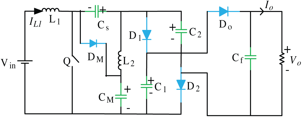
Figure 1: Circuit diagram of the proposed converter
The circuit diagram of the proposed converter is shown in Fig. 1. The equivalent circuit diagrams during different modes of operation of the proposed converter are shown in Fig. 2. When switch ‘Q’ is ON, the equivalent circuit diagram is shown in Fig. 2a. During this mode, the inductors L1 stores energy from the supply, and L2 stores energy from the difference of voltage across the capacitor Cs and CM. The series-connected switched capacitor cells C1 and C2 supplies energy to the load. When switch ‘Q’ is OFF, as shown in Fig. 2b, the switched capacitors C1, C2, and CM are charged by both the inductors L1 and L2. The available voltage at switched capacitors C1 and C2 are equal as they are connected in parallel. Let the voltage across the capacitor Cs, CM, and C1 be Vcs, VCM, and Vceq, respectively, the voltage across the switch ‘Q’ be VQ, the current through the inductor L1 be IL1 and load current be Io. The waveforms of the proposed converter in continuous conduction mode (CCM) are depicted in Fig. 3. Fig. 4 shows the component waveforms of the proposed converter.
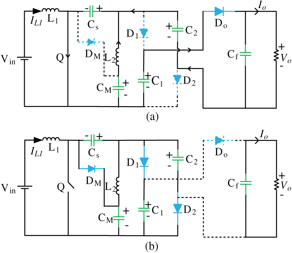
Figure 2: Operation of the converter (a) ON state of ‘Q’. (b) OFF state of ‘Q’
The steady-state analysis requires that the voltage across the inductor L1 during each switching cycle should be zero, hence:


Similarly, for inductor L2 net voltage across it during each switching cycle is zero, hence:
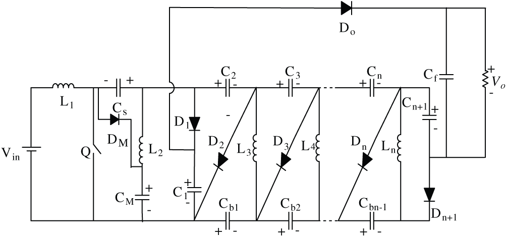
Figure 3: Proposed converter with ‘n’ times multiplier cells

During the OFF state of the switch ‘Q’,


From the above equations,

From Eqs. (2) and (7), the voltage across the switch is presented as follows.

where VD1, VD2, VDM, VD0 are the voltages across the diodes D1, D2, DM, and D0. Similarly, the voltage gain by considering only three inductors L1, L2, and L3 is given in Eq. (9).

Similarly, for the converter having ‘n’ number of voltage multiplier cells, as shown in Fig. 3, the output voltage is given in Eq. (10).

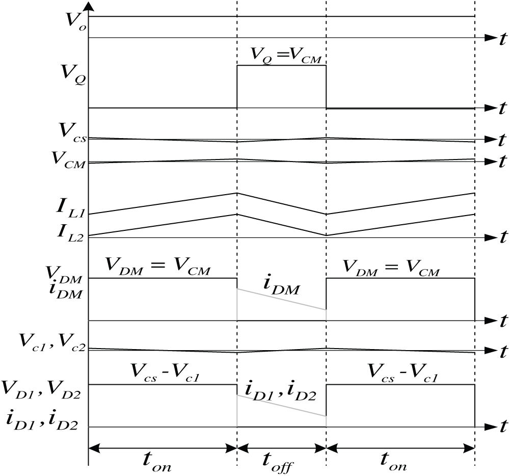
Figure 4: Operational typical waveforms of proposed converter
3 Design of Circuit Parameters
The design of circuit parameters for the proposed converter is as follows.
Allowing 9% of ripples in the input current, the inductor value can be designed based on the following expression.

For the same input and output power, i.e., and using Eq. (7), the average and root mean square (RMS) value of inductor current expression for computing the copper losses in the inductor is given by,

Considering ripple current to be symmetrical and triangular, the RMS value for a triangular wave DC offset is expressed as follows.

The expression for the value of inductor L2 is the same as that of inductor L1. But, the current in inductor L1 represents the average input current, and the current through the inductor L2 represents the output current. The value of second inductor L2 is not equal to input inductor value L1, but has a value half of the input inductor value as the current through the second inductor L2 is significantly less than the input current.
The switched capacitors Cs, CM, C1, and C2, need to allow a change in the charge and, therefore, input voltages. So the value of these capacitors needs to be small to allow the variations. The load current flows through these capacitors during the ON position of the switch. With 1% of voltage ripple, their value capacitance C is expressed as:

where fsw = Switching frequency. The selection of output capacitors Co is made considering voltage ripple ∆VO max to be 1%.

4 Simulation Study of Proposed Converter
Simulation studies for the proposed converter have been carried out on the MATLAB/SIMULINK platform with an input voltage of 30 V, 100 W load at a switching frequency of 20 kHz. The performance of the converter is carried out with the average current controller. The average current control technique has two loops. One is the outer loop to control the output voltage, and the second one is the inner loop to control the input current. The error from the current controller is compared with the carrier signal and generates the required pulse to the switch.
The performance analysis of the proposed converter is carried out at
1. Steady-state simulation study and
2. Dynamic-state simulation study
4.1 Steady-State Simulation Study
The steady-state simulation study has been done based on the circuit parameters mentioned in Tab. 1. The simulation results of the proposed converter with parameters such as load current (IL1), output voltage (Vo), and the voltage across the switch (VQ) are plotted. Fig. 5 shows the simulation results of the proposed converter with a duty ratio of 0.781 for the output voltage of 380 V with a switching frequency of 20 kHz.
Table 1: Proposed converter parameters for simulation study
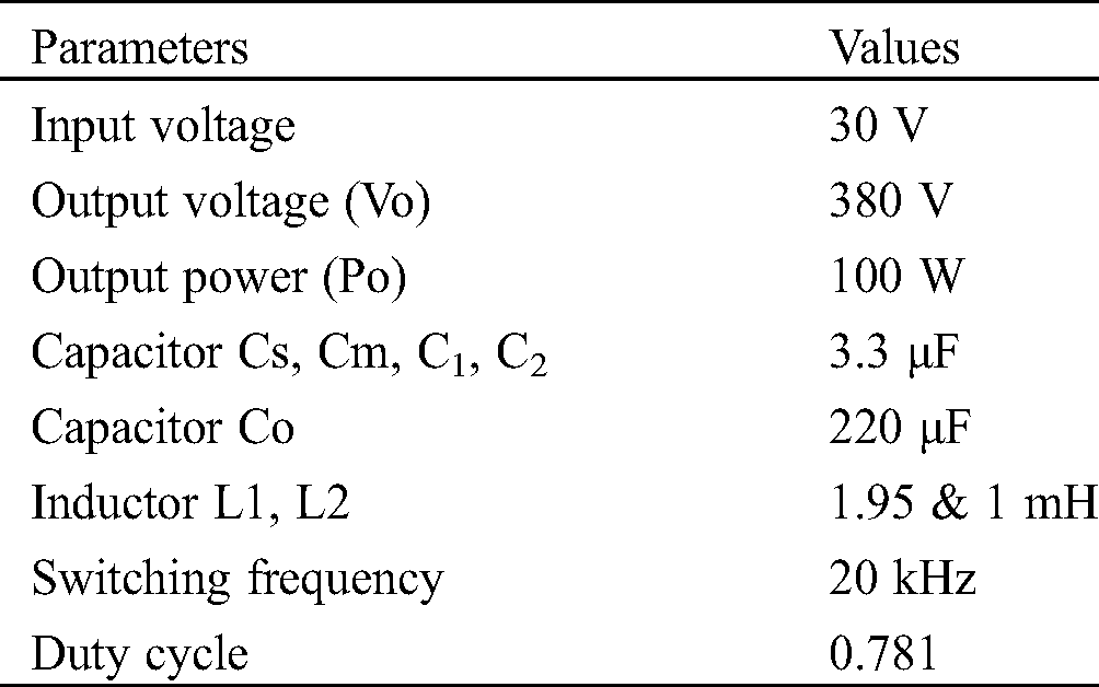
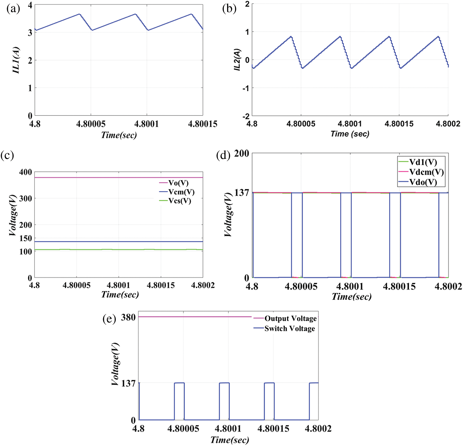
Figure 5: Simulation results of proposed converter for (a) inductor current (IL1). (b) Inductor current (IL2). (c) Voltage across capacitors Cf, Cs, Cm. (d) Voltage across diodes Da, Dm and Do. (e) Output voltage (Vo). Switch voltage (VQ)
Fig. 5a depicts the simulated waveform of input Inductor current (IL1) with respect to time on the x-axis. The input power drawn from the 30 V source is 100 W. It can be pointed out that the inductor current (IL1) waveform has an average value of 3.33 A. The peak-peak value of the inductor current (IL1) is 0.6 A based on the design values. It is observed that the input current is continuous in nature, which is essential, particularly in solar applications. Fig. 5b depicts the simulated waveform of the second inductor current (IL2). The second inductor current has a peak value of 0.6 A, and its average current is equal to the load current. The peak current of 0.6 A of the second inductor is due to considering half of the input inductor value. Its value is half of the input inductor because the average current that passes through this inductor is equal to load current, which is a very small value, i.e., 0.263 A. In Fig. 5c, the voltage across capacitors Cs, Cm, and Cf are shown. The value of voltage across the capacitor CM (Vcm) is around 136.69 V and across capacitor Cs (Vcs) is approximately 106.72 V. The desired output voltage is 380 V. Based on Eqs. (4) and (6), the output voltage is the sum of 2Vcm and Vcs and is satisfied. Fig. 5d shows the voltage across the diodes D1, DM, and D0 during their OFF state. The voltage that appears across these diodes is 136.69 V satisfying the Eq. (8). It can be observed that the reverse-biased voltage across the diodes is much less as compared to the output voltage of 380 V. Fig. 5e shows the output voltage (Vo) and switch voltage (VQ). The voltage across the switch is 136.69 V satisfying Eq. (8). The reversed biased voltage that appears across the switch during the OFF state is much less as compared to the output voltage. The desired output voltage 380 V is achieved with an average current control technique, as shown in the waveform. Therefore a lesser voltage rating of diodes and switches can be implemented, which results in a decrease in cost.
4.2 Dynamic State Simulation Study
The dynamic state simulation studies were performed on MATLAB/SIMULINK in the following lines.
Case 1: By considering the variation in the load from 100% to 50%.
Case 2: By considering the variation in the load from 50% to 100%.
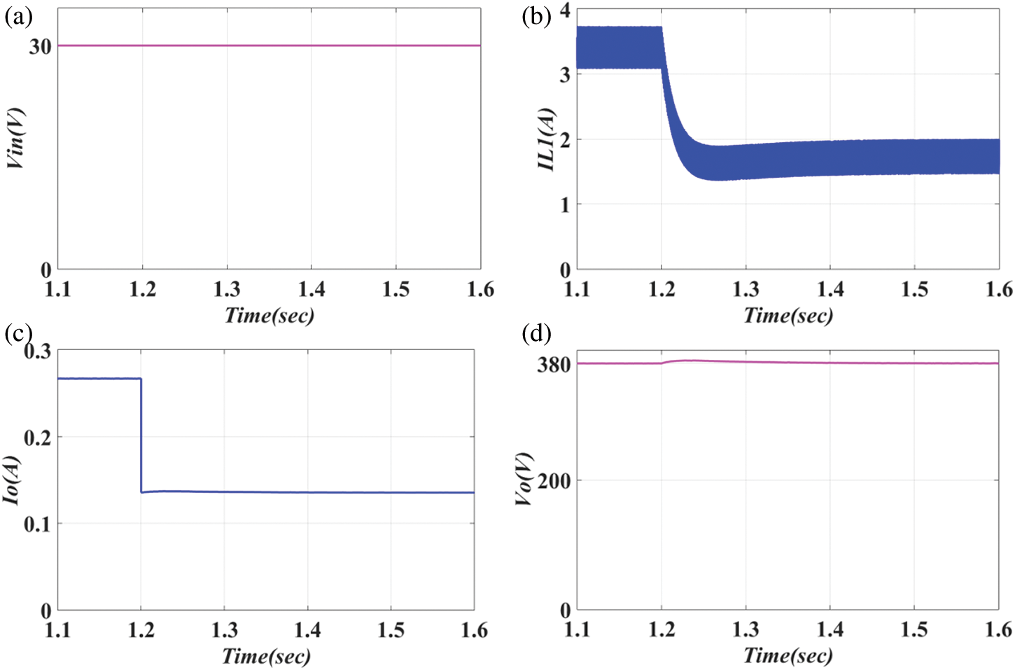
Figure 6: Simulated results of proposed converter for load variation from 100% to 50%. (a) Input voltage (Vin). (b) Inductor current (IL1). (c) Output current (Io). (d) Output voltage (Vo)
Case 1: Considering the Variation in the Load from 100% to 50%
The dynamic state simulation study of the proposed converter has been done by varying the load from 100% to 50% at a simulation time of 1.2 s. The closed-loop operation of the proposed converter with the average current method is implemented in the dynamic state study. The MATLAB/SIMULINK results are shown in Fig. 6. Fig. 6a shows the waveform for input voltage (Vin). The input voltage is constant during the dynamic change in the load from 100% to 50%. It means that the input voltage to the converter is not affected during its dynamic state. Fig. 6b shows the waveform for inductor current (IL1). The value of the inductor current is 3.33 A at 100 W output power. Its value is 1.67 A at 50 W output power. As the load is varied from 100% to 50%, the inductor current (IL1) is changed from the average value of 3.33 to 1.67 A. The inductor current (IL1) is settled to 1.67 A at 1.55 s. The inductor current is well controlled by the inner loop current controller in the average current control method. Fig. 6c shows the waveform for load current (Io). The value of load current (Io) at 100 W load is 0.263 A. During the dynamic change in the load from 100% to 50%, the load current (Io) is changed from 0.263 to 0.132 A. The load current (Io) is settled to 0.132 A at 1.55 s. Fig. 6d shows the waveform for output voltage (Vo). During the dynamic change in the load from 100% to 50%, the output voltage (Vo) has a surge, and its value is about 385 V. The output voltage is settled to 380 V at 1.55 s. The control of output voltage is well regulated by the outer loop voltage controller in the average current control method.
Case 2: Considering the Variation in the Load from 50% to 100%
Fig. 7a shows the waveform of input voltage (Vin). The input voltage is constant during the dynamic change in the load from 50% to 100%. It means that the operation of the converter is not affecting the input voltage applied. Fig. 7b shows the waveform for inductor current (IL1). As the load is varied from 50% to 100%, the inductor current (IL1) is changed from the average value of 1.67 to 3.33 A. The inductor current (IL1) is settled to 3.33 A at 1.55 s. The input inductor current is controlled by the current controller in the inner loop of the average current controller. Fig. 7c shows the waveform for load current (Io). The value of load current (Io) at 50 W load is 0.132 A. During the dynamic change in the load from 50% to 100%, the load current (Io) is changed from 0.132 to 0.263 A. The load current (Io) is settled to 0.263 A at 1.55 s. Fig. 7d shows the waveform for output voltage (Vo). During the dynamic change in the load from 50% to 100%, the output voltage (Vo) has a sag, and its value is about 375 V. The output voltage is settled to 380 V at 1.55 s. The desired output voltage 380 V is achieved with the voltage controller in the outer loop of the average current controller.
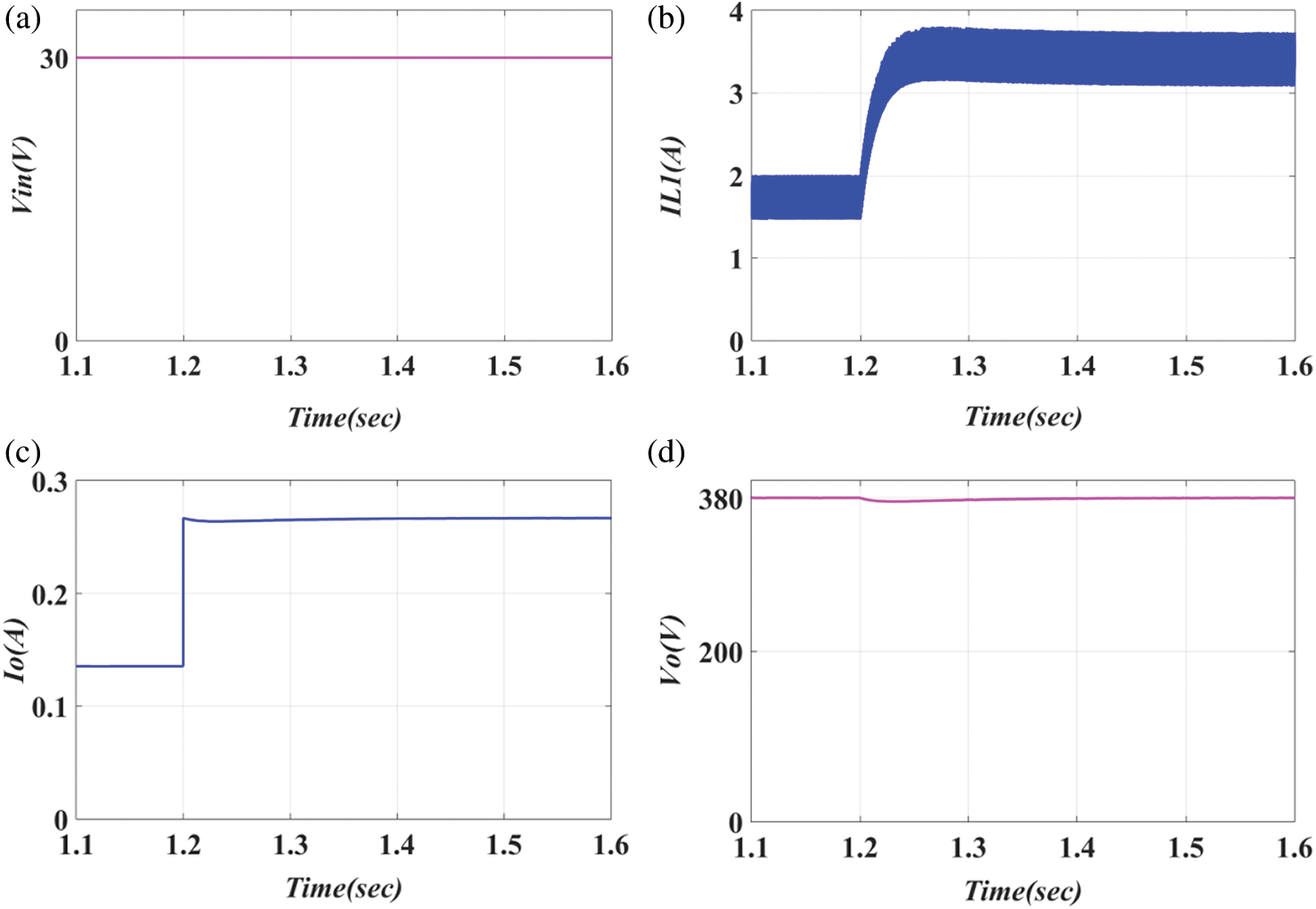
Figure 7: Simulated results of proposed converter for load variation from 50% to 100%. (a) Input voltage (Vin). (b) Inductor current (IL1). (c) Output current (Io). (d) Output voltage (Vo)
The dynamic state simulation study of the proposed converter has been done by varying the load from 50% to 100% at a simulation time of 1.2 s. The MATLAB/SIMULINK results are shown in Fig. 7.
Table 2: Comparison of different converters
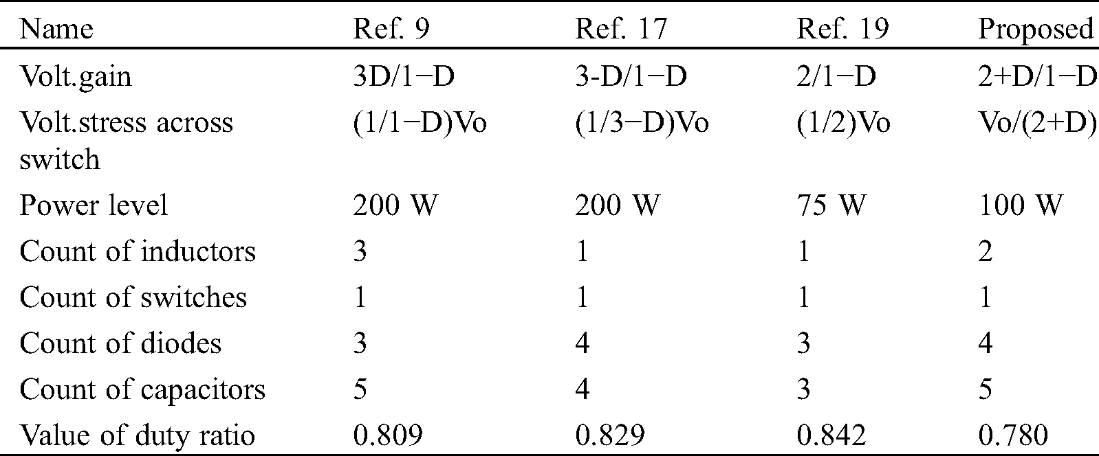
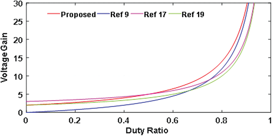
Figure 8: Comparison of gain with different converters
Tab. 2 shows the overall comparison of other DC-DC converters with the proposed topology. Fig. 8 depicts the plot of various converters with voltage gain and duty ratio. Tab. 2 and Fig. 8 shows that the proposed converter has more gain. DC-DC converters [9,17,19] have less gain compared to the proposed topology. It can also be said that the reverse bias voltage across the elements is less in the proposed converter. The voltage stress across the switch based on their duty ratio for [9] is 1,989 V, [17] is 175.03, [19] is 190 V and for the proposed converter is 136.69 V. The same is verified in the simulation result for the proposed converter. Also, in the proposed converter, the voltage stress across all the diodes is 136.69 V, which is the same as the voltage stress across the switch, as shown in the results based on the Eq. (8). From Eq. (11), the change in inductor current or inductor ripple current is directly proportional to the duty ratio. If the duty ratio is less, then the ripple current will be less and vice versa. From Tab. 2, the duty ratio of the proposed converter is less compared to remaining converters; therefore, the ripple current for the proposed converter is less as compared to remaining converters. So, all the features such as ripple current, high gain, and less voltage stress are verified.
The high voltage needed in DC bus for inverter input can be accomplished with proposed high-gain DC converters utilizing the photovoltaic (PV) or fuel cell as a source. The design of switched-capacitor cells performs the boosting operation. The switched capacitor produces significant static gains while simultaneously limiting the voltage stress of the various components. This converter can be able to
1. It has continuous input current from the source with reduced ripples in the input current.
2. It has a single switch with reduced voltage devices, resulting in a low cost to build the converter.
3. The closed-loop operation proves that the output voltage can be well regulated.
The operation of the proposed converter with steady-state and dynamic state analysis was discussed. This new topology with a switched capacitor is implemented to accomplish all the features such as one switch, high gain with continuous current from the source, and, therefore, can be implemented in renewable energy applications. All these features are validated through MATLAB/SIMULINK.
Funding Statement: The author(s) received no specific funding for this study.
Conflicts of Interest:The authors declare that they have no conflicts of interest to report regarding the present study.
1. Tan, K., Song, X. Q., Peng, C., Liu, P. K., Huang, A. Q. (2016). Hierarchical protection architecture for 380 V DC data center application. Proc. Energy Conversion Congress and Exposition, Milwaukee, Wi, 1–8. DOI 10.1109/ECCE.2016.7855145. [Google Scholar] [CrossRef]
2. Boroyevich, D., Cvetkovic, I., Burgos, R., Dong, D. (2013). Intergrid: A future electronics energy network. IEEE Journal of Emerging and Selected Topics in Power Electronics, 1(3), 127–138. DOI 10.1109/JESTPE.2013.2276937. [Google Scholar] [CrossRef]
3. Li, W., He, X. (2011). Review of non-isolated high step-up DC/DC converters in photovoltaic grid connected applications. IEEE Transactions on Industrial Electronics, 58(4), 1239–1250. DOI 10.1109/TIE.2010.2049715. [Google Scholar] [CrossRef]
4. Wu, T. F., Yu, T. H. (1998). Unified approach to developing single-stage power converters. IEEE Transactions on Aerospace and Electronic Systems, 34(1), 211–223. DOI 10.1109/7.640279. [Google Scholar] [CrossRef]
5. Premkumar, M., Subramaniam, U., Haes Alhelou, H., Siano, P. (2020). Design and development of non-isolated modified SEPIC DC-DC converter topology for high-step-up applications: Investigation and hardware implementation. Energies, 13(15), 3960. DOI 10.3390/en13153960. [Google Scholar] [CrossRef]
6. Wai, R. J., Lin, C. Y., Duan, R. Y., Chang, Y. R. (2007). High-efficiency DC-DC converter with high voltage gain and reduced switch stress. IEEE Transactions on Industrial Electronics, 54(1), 354–364. DOI 10.1109/TIE.2006.888794. [Google Scholar] [CrossRef]
7. Premkumar, M., Kumar, C., Anbarasan, A., Sowmya, R. (2020). A novel non-isolated high step-up DC–DC boost converter using single switch for renewable energy systems. Electrical Engineering, 102(2), 811–829. DOI 10.1007/s00202-019-00904-8. [Google Scholar] [CrossRef]
8. Wu, T. F., Lai, Y. S., Hung, J. C., Chen, Y. M. (2008). Boost converter with coupled inductors and buck–boost type of active clamp. IEEE Transactions on Industrial Electronics, 55(1), 154–162. DOI 10.1109/TIE.2007.903925. [Google Scholar] [CrossRef]
9. Bonab, H. A. F., Banaei, M. R. (2020). Enhanced buck-boost dc–dc converter with positive output voltage. Journal of Circuits, Systems and Computers, 29(5), 2050072. DOI 10.1142/S0218126620500723. [Google Scholar] [CrossRef]
10. Prudente, M., Pfitscher, L. L., Emmendoerfer, G., Romaneli, E. F., Gules, R. (2008). Voltage multiplier cells applied to non-isolated DC–DC converters. IEEE Transactions on Power Electronics, 23(2), 871–887. DOI 10.1109/TPEL.2007.915762. [Google Scholar] [CrossRef]
11. Axelrod, B., Berkovich, Y., Ioinovici, A. (2008). Switched-capacitor/switched-inductor structures for getting transformerless hybrid DC–DC PWM converters. IEEE Transactions on Circuits and Systems I: Regular Papers, 55(2), 687–696. DOI 10.1109/TCSI.2008.916403.
12. Premkumar, M., Kumar, C., Sowmya, R. (2019). Analysis and implementation of high-performance DC-DC step-up converter for multilevel boost structure. Frontiers in Energy Research, 7, 1147. DOI 10.3389/fenrg.2019.00149. [Google Scholar] [CrossRef]
13. Maalandish, M., Hosseini, S. H., Jalilzadeh, T. (2018). High step-up dc/dc converter using switch-capacitor techniques and lower losses for renewable energy applications. IET Power Electronics, 11(10), 1718–1729. DOI 10.1049/iet-pel.2017.0752. [Google Scholar] [CrossRef]
14. Wu, B., Li, S., Smedley, K. M., Singer, S. (2015). A family of two switch boosting switched-capacitor converters. IEEE Transactions on Power Electronics, 30(10), 5413–5424. DOI 10.1109/TPEL.2014.2375311. [Google Scholar] [CrossRef]
15. Ioinovici, A. (2001). Switched-capacitor power electronics circuits. IEEE Circuits and Systems Magazine, 1(3), 37–42. DOI 10.1109/7384.963467. [Google Scholar] [CrossRef]
16. Zamiri, E., Vosoughi, N., Hosseini, S. H., Barzegarkhoo, R., Sabahi, M. (2016). A new cascaded switched capacitor multilevel inverter based on improved series–parallel conversion with less number of components. IEEE Transactions on Industrial Electronics, 63(6), 3582–3594. DOI 10.1109/TIE.2016.2529563. [Google Scholar] [CrossRef]
17. Wu, B., Li, S., Liu, Y., Smedley, K. M. (2016). A new hybrid boosting converter for renewable energy applications. IEEE Transactions on Power Electronics, 31(2), 1203–1215. DOI 10.1109/TPEL.2015.2420994. [Google Scholar] [CrossRef]
18. Kishore, G. I., Tripathi, R. K. (2020). High gain single switch DC-DC converter based on switched-capacitor cells. Journal of Circuits, Systems and Computers, 29(12), 2050188. DOI 10.1142/S0218126620501881. [Google Scholar] [CrossRef]
19. Kishore, G. I., Tripathi, R. K. (2020). Single-phase unidirectional AC-DC PFC converter with switched capacitors. International Journal of Electronics, 30(10), 1–17. DOI 10.1080/00207217.2020.1793401. [Google Scholar] [CrossRef]
 | This work is licensed under a Creative Commons Attribution 4.0 International License, which permits unrestricted use, distribution, and reproduction in any medium, provided the original work is properly cited. |