| Energy Engineering |
DOI: 10.32604/ee.2022.017556
ARTICLE
Research on Phase-Shifted Full-Bridge Circuit Based on Frequency and Phase-Shift Synthesis Modulation Strategy
1Key Laboratory of Smart Grid of Education Ministry, Tianjin University, Tianjin, China
2Electric Power Research Institute of Yunnan Power Grid Co., Ltd., Kunming, China
*Corresponding Author: Hongfeng Li. Email: lab538@163.com
Received: 20 May 2021; Accepted: 23 July 2021
Abstract: The full-bridge converters usually use transformer leakage inductance and parallel resonant capacitors to achieve smooth current commutation and soft switching functions, which can easily cause problems such as energy leakage and significant duty cycle loss. This paper designs a novel full-bridge zero-current (FB-ZCS) converter with series resonant capacitors and proposes a frequency and phase-shift synthesis modulation (FPSSM) control strategy based on this topology. Compared with the traditional parallel resonant capacitor circuit, the passive components used are significantly reduced, the structure is simple, and there is only a slight energy loss. By controlling the charging time of the capacitor, it can be achieved without additional switches or auxiliary circuits. The automatic control of capacitor energy based on input current addresses the low efficiency of the traditional control strategies. This paper introduces its principle in detail and verifies it through simulation. Finally, an experimental prototype was built further to demonstrate the feasibility of the theory through experiments. The module can be applied to a photovoltaic DC collection system using input parallel output series (IPOS) cascade to provide a new topology for large-scale, long-distance DC transmission.
Keywords: Full-bridge converter; frequency and phase-shift synthesis modulation (FPSSM); photovoltaic DC collection system; control strategy
With the increasing energy crisis and environmental pollution, photovoltaic power generation has been vigorously promoted. Photovoltaic grid-connected inverter converts the DC power output by photovoltaic modules into AC power that meets the requirements of the grid and then inputs it to the grid. It is the core of grid-connected photovoltaic system energy conversion and control, and it is currently the most widely used full-bridge DC-DC converter. With the increasing requirements for the volume and efficiency of power conversion modules, the switching frequency of phase-shifted full-bridge DC-DC converters is getting higher and higher. However, existing full-bridge converters usually use transformer leakage inductance and parallel resonant capacitors to realize smooth current commutation and soft switching functions [1], as shown in Fig. 1.
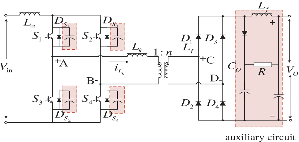
Figure 1: Existing DC boost converter topology
Parallel resonance capacitors have the following disadvantages:
1) The energy stored in the capacitor is fixed. When the load is reduced, it will cause excess energy, which will affect the adjustment range and reduce the operating efficiency of the system;
2) The parallel resonant capacitor needs a dedicated capacitor charging interval during each switching cycle, which will cause the duty cycle loss;
3) With the decrease of the load, the duty cycle loss will increase significantly, and the input current will decrease, and the capacitor charging time will be longer [2];
4) The parallel resonant capacitor will form an energy leakage channel through the transformer winding. The energy stored in the capacitor must exceed the rated value to compensate for the energy loss, but too much energy will further aggravate the energy leakage.
Input parallel output series (IPOS) to increase the output voltage level and power level while reducing the voltage and current stress of the switch tube in the circuit. It is suitable for high-power applications requiring high voltage gain and has gained popularity in recent years. More benefits of IPOS structure include reduced input current and output voltage of each module, module shedding capability, reduced ripple content due to interleaving, intrinsic balancing, and scalable control method. Li et al. [3] proposed a modular isolated soft-switching DC–DC converter that can offer two levels of fault tolerance. The converter consists of an IPOS connected modules to boost voltage levels for High-Power High-Voltage Applications. Likewise, Ye et al. [4] present a novel double-coupled inductor and voltage multiplier boost converter with input parallel output series modules, inheriting the advantages of interleaved series output capacitors with high voltage gain and low output voltage ripple for photovoltaic and fuel cell energy systems, high-intensity discharge lamps (HID), DC backup energy systems, and electric vehicles.
The above shortcomings will affect the maximum power point tracking (MPPT) range and conversion efficiency of the photovoltaic system and significantly impact the adjustment and operating range of the converter. Edwin et al. [5] propose a coupled inductance soft-switching high-gain DC-DC converter. By adding active clamps on the input side to alleviate the switching tube voltage spike problem caused by leakage inductance, it can also realize that the main and auxiliary switches work in soft-switching mode. However, the current ripple on the input side is significant. Similarly, The voltage doubling function of the switched capacitor to obtain a very high voltage transmission ratio is used in [6]. However, the isolated converter still has the disadvantages of considerable input current pulse, insufficient output voltage stabilizing ability, and low load adjustment rate. Furthermore, Shi et al. [7,8] proposed a DC-DC converter with a source soft-switching auxiliary circuit on the secondary side based on the parallel resonant circuit, which solved voltage stabilization, realized high-frequency soft switching, and improved the working efficiency. However, the control method becomes more complicated due to the increase in the number of switch tubes.
Frequency and phase-shift synthesis modulation technology (FPSSM) is widely used in aviation, wireless communication, and other fields. Azim et al. [9] utilize FPSSM technology for energy-efficient optical wireless systems with direct current (DC) offset hybrid frequency and phase shift keying (DC-FPSK) modulation for Internet-of-Things based on optical wireless systems resulting in higher modulation rates and greater flexibility. An FPSSM signal optical generation technique is proposed in [10], which uses a polarization-preserving fiber Bragg grating with different responses to different input polarization states to convert the baseband information loaded into the signal polarization state to that of the output wavelength, and achieves frequency modulation by interpolation of the beat frequency at the receiver side. It solves the problem that the traditional dual-source beat frequency introduces large phase noise and improves the communication quality of the edge nodes of the cellular communication system. However, in power electronics, this technology has been studied by a few people. Hu et al. [11] apply the phase-shifting frequency conversion technique to a dual active bridge converter to ensure zero-voltage switching over a wide power range with minimal circulating current but does not discuss the use of phase drift compensation in the zero-sequence modulation scheme and the option of combining variable-frequency modulation (VFM) with conventional zero-sequence modulation. A novel variable frequency dual-phase shift synthesis modulation method is designed in [12] and applied in a full-bridge three-level LLC resonant converter. It is demonstrated that the proposed modulation method can achieve soft switching of all switching tubes in the whole load range, but the efficiency and reliability of its operation are not further discussed. This paper applies this technique to a full-bridge zero-current (FB-ZCS) converter, and a prototype is built to discuss its reliability.
This paper designs a full-bridge boost converter with series resonant capacitors, which controls the charging time of the capacitor through frequency and phase-shift synthesis modulation, and automatic control of capacitor energy based on input current can be achieved without the need for additional switches or auxiliary circuits. Compared with the traditional parallel resonant capacitor circuit, the passive components used are significantly reduced, the structure is simple, and have a small energy loss. At the same time, the series capacitor solves the problem of energy leakage in the transformer winding during circulating current, which improves the equipment efficiency.
The proposed full-bridge zero-current switching (FB-ZCS) converter is shown in Fig. 2. The primary side is composed of four reverse blocking switches S1--S4 to form a full-bridge circuit. The reverse blocking switch is realized by a package module in which IGBTs and diodes are connected in parallel. It is used to remove the discharge path of the resonant capacitor in a high-frequency circuit. The converter input inductance
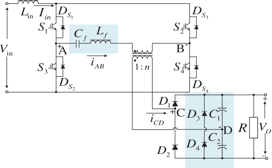
Figure 2: The proposed DC boost converter topology
The secondary circuit is composed of a voltage doubler rectifier, which is composed of a group of diodes
The advantages of this topology are as follows:
1) There is an inductance on the low-voltage input side to minimize voltage stress and insulation requirements. At the same time, the input inductance as a constant current source can alleviate the problem of transformer flux balance and saturation;
2) The leakage inductance of the transformer replaces the additional clamp circuit so that the circuit can smoothly commutate current without voltage spikes.
3) During the entire working cycle, the zero-current switching (ZCS) of the primary side switches and the zero-voltage switching (ZVS) or ZCS of the secondary side diode reduces the switching loss, thereby improving the system efficiency.
4) The passive components used are reduced, the secondary side does not need auxiliary components, the overall structure is simple, and the loss is reduced.
The working sequence of the converter is shown in Fig. 3. The switching tubes
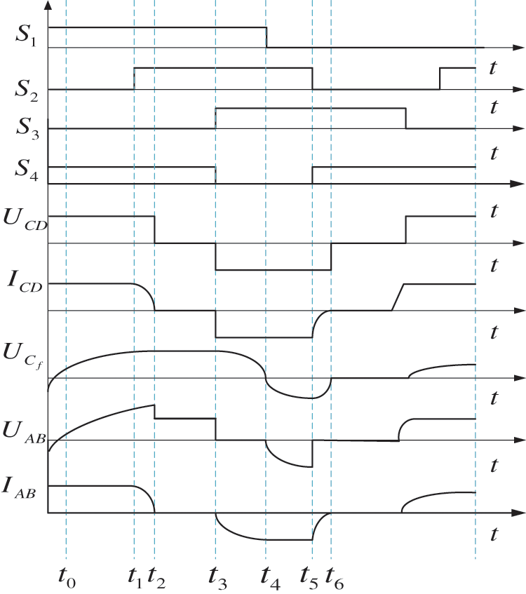
Figure 3: The timing diagram of the converter
To facilitate steady-state analysis, the following assumptions are made:
1) All components in the circuit are ideal;
2) The input inductance
3) The transformer magnetizing inductance is large.
Eq. (1) denotes the resonance frequency (
The steady-state operation of the circuit in a complete cycle is divided into twelve modes. The first four modes are described in detail according to the working timing waveforms, as shown in Fig. 3. Fig. 4 lists the first six modes of operation, and the following six modes can be discussed similarly for periodic symmetry.
(1) Mode-I (
When the current
where
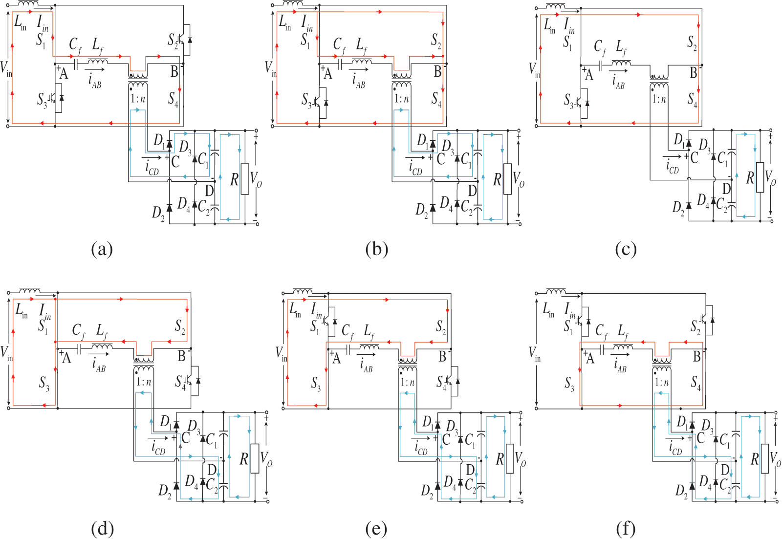
Figure 4: The first six working modes (a) working mode I (b) working mode II (c) working mode III (d) working mode IV (e) working mode V (f) working mode VI
(2) Mode II (
After
where
(3) Mode III (
At this time, the current of S1 completely turns to S2 and forms a loop with
(4) Mode IV (
In this mode,
(5) Mode V (
In this mode,
(6) Mode VI (
In this mode, S2 is also closed; the current
3 Application in the Control of Photovoltaic Power Generation
As shown in Fig. 5, in practical applications, the FB-ZCS topology adopts the form of sub-module input parallel output series (IPOS) to increase the output voltage level and power level [19–21] and reduce the voltage and current stress of the switch tube in the circuit.
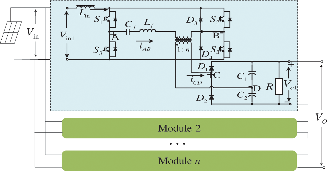
Figure 5: IPOS cascaded DC–DC converter topology
3.1 Frequency and Phase-Shift Synthesis Modulation (FPSSM) Control Strategy
In this paper, the control strategy is shown in Fig. 6, and the conductance increment method is used to achieve maximum power tracking (MPPT). The PI controller modulates the difference between the reference voltage
During the normal operation of the circuit, the load reduction will cause the input current
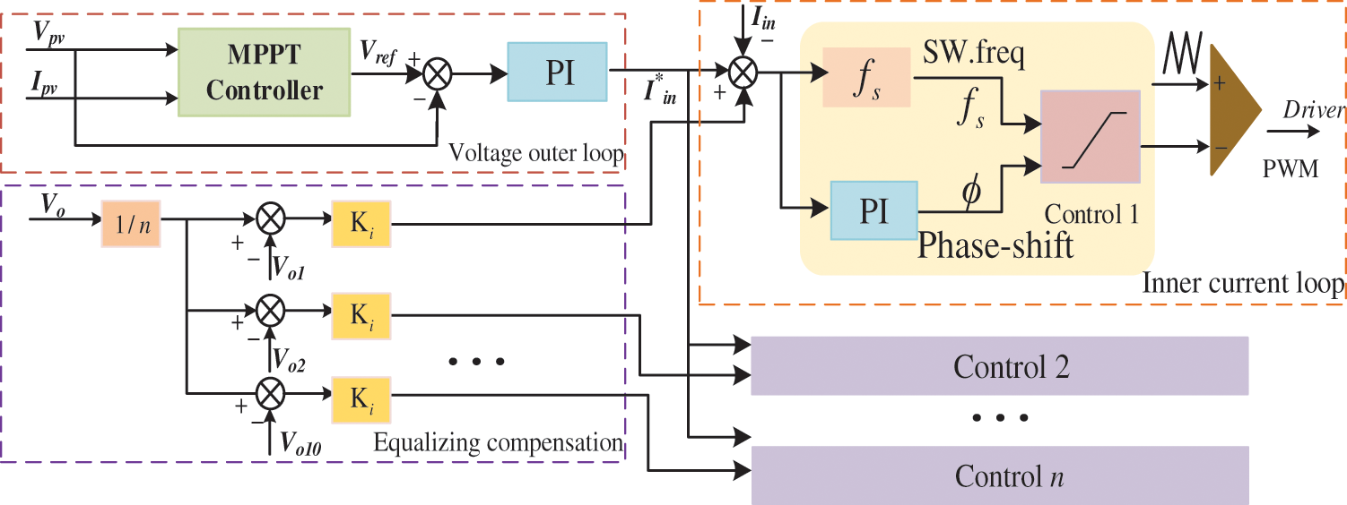
Figure 6: FB-ZCS input current control
Analyzing the working mode, the research concluded that energy is transferred from the input side to the output side during Mode I while charging the capacitor
Since the duty cycle D is relatively consistent with the conventional duty cycle, the
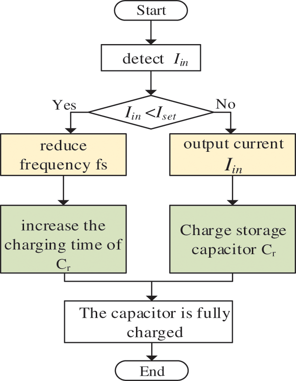
Figure 7: Mode switching flowchart
If
From the analysis in Section 2.2, to achieve smooth current commutation and soft switching, the energy stored in the
The energy stored in
where
Table 1 shows the comparison of the proposed topology with other literature topologies [23–25], where converters require longer charging time to full load rating, which is an unnecessarily light load. These structures have the following advantages: the existence of a low-voltage input side inductor minimizes the voltage stress and insulation requirements; the input inductor can also be used as a constant current source to alleviate the flow balance and saturation problems of the transformer.
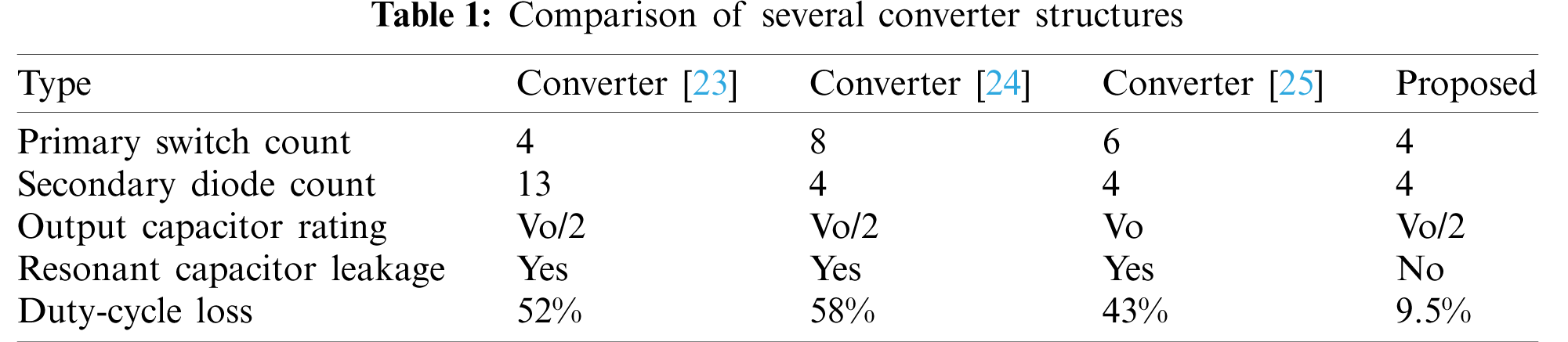
As a result, the duty cycle loss of existing converters is more than 50% of the switching time period, which severely limits the operating range of the converter. In contrast, the topology in this paper uses series capacitors and FPSSM control to reduce unnecessary charging intervals and duty cycle losses to 10%. Through comparison, it can be concluded that the proposed structure is more compact and has better performance.
The proposed control strategies were verified separately, and 10 IPOS cascaded FB-ZCS DC boost converter models were built in MATLAB, and their parameter settings are shown in Table 2.
Next, the verification process of the topology and control strategy is proposed.
4.1 Stability Analysis of Output Voltage and Current
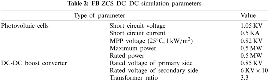
Due to a pair of clamping diodes that are attached to the secondary side, the energy generated by the parasitic oscillation of the secondary side is fed back to the primary side, and the oscillation and voltage spikes are suppressed so that high-frequency oscillation and voltage overshoot of the secondary stage of the transformer is effectively suppressed. Fig. 8 shows the voltage waveforms of the primary side of the transformer of the traditional DC boost converter and the proposed DC boost converter, respectively. Through comparison, it can be observed that the high-frequency oscillation of the transformer secondary side is restrained, and voltage overshoot is prevented in the process of switching on and off.
The input and output voltage and current of a single FB-ZCS sub-module are shown in Fig. 9. The analysis shows that the voltage and current enter a stable operating state after a short period of fluctuation. After stabilization, the output voltage ripple coefficient is
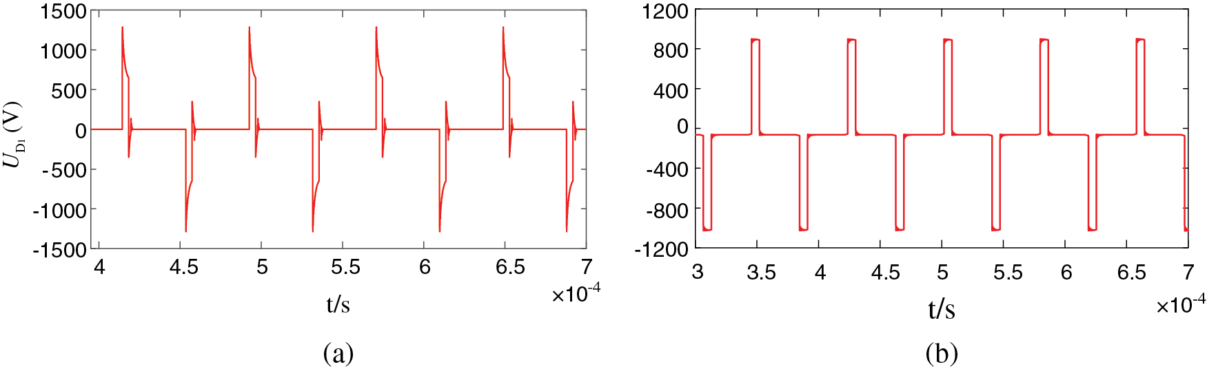
Figure 8: Voltage waveform of the secondary side. (a) Traditional DC boost converter; (b) The proposed DC boost converter
Figure 9: Single FB-ZCS input and output voltage and current waveform diagram and partially enlarged view. (a) Input voltage waveform and partial enlarged view; (b) Output voltage waveform and partial enlarged view; (c) Input current waveform and partial enlarged view; (d) Output current waveform and partial enlarged view
4.2 Frequency and Phase-Shift Synthesis Control
Fig. 10 shows the input and output waveforms of
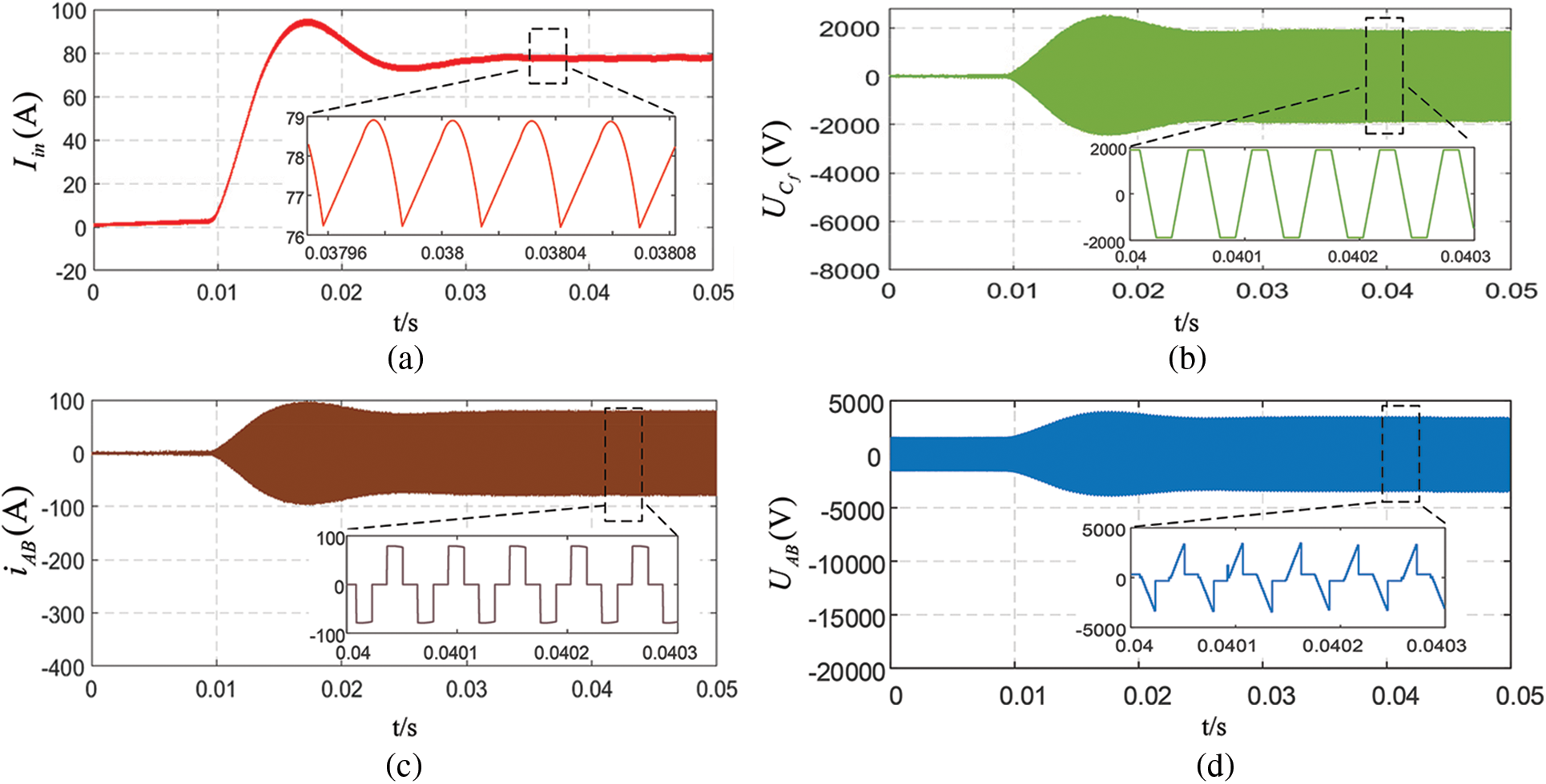
Figure 10: Input and output waveform and partially enlarged diagram. (a) Iin waveform and partial enlarged view; (b)
According to the radiation characteristics of photovoltaic cells, as the light irradiance decreases, the voltage and current output by photovoltaic modules gradually decrease. Set the initial light irradiance of the photovoltaic module to
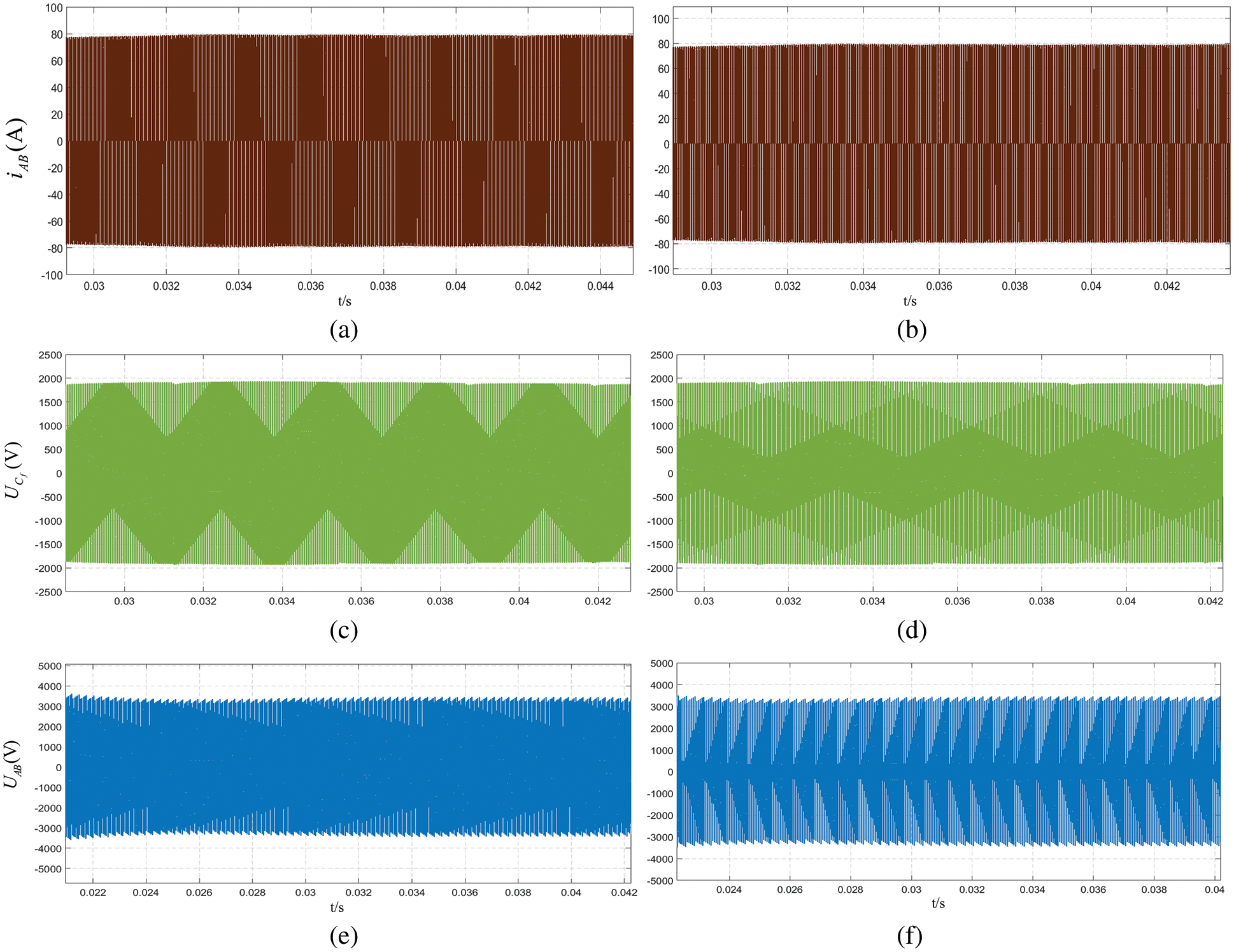
Figure 11: Waveform diagram of the primary voltage and capacitor voltage. (a) Light irradiance 550 W/m2 fs = 18 KHZ; (b) Light irradiance 1000 W/m2 fs = 21 KHZ; (c) Light irradiance 550 W/m2 fs = 18 KHZ; (d) Light irradiance 1000 W/m2 fs = 21 KHZ; (e) Light irradiance 550 W/m2 fs = 18 KHZ; (f) Light irradiance 1000 W/m2 fs = 21 KHZ
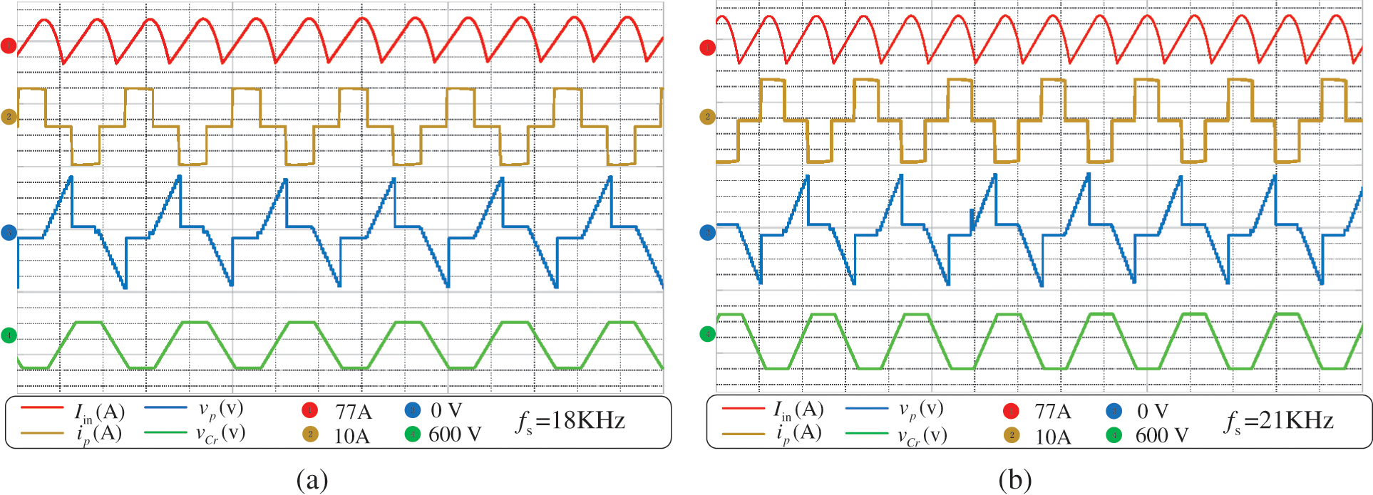
Figure 12: Partially enlarged simulation waveform. (a) Light irradiance 550 W/m2; (b) Light irradiance 1000 W/m2
When the light irradiance is within
The light irradiance of the photovoltaic module is reduced to
Taking the ZCS turn-on process of S1 in Mode IV as an example for analysis. Fig. 13 shows the simulation waveform of the switching
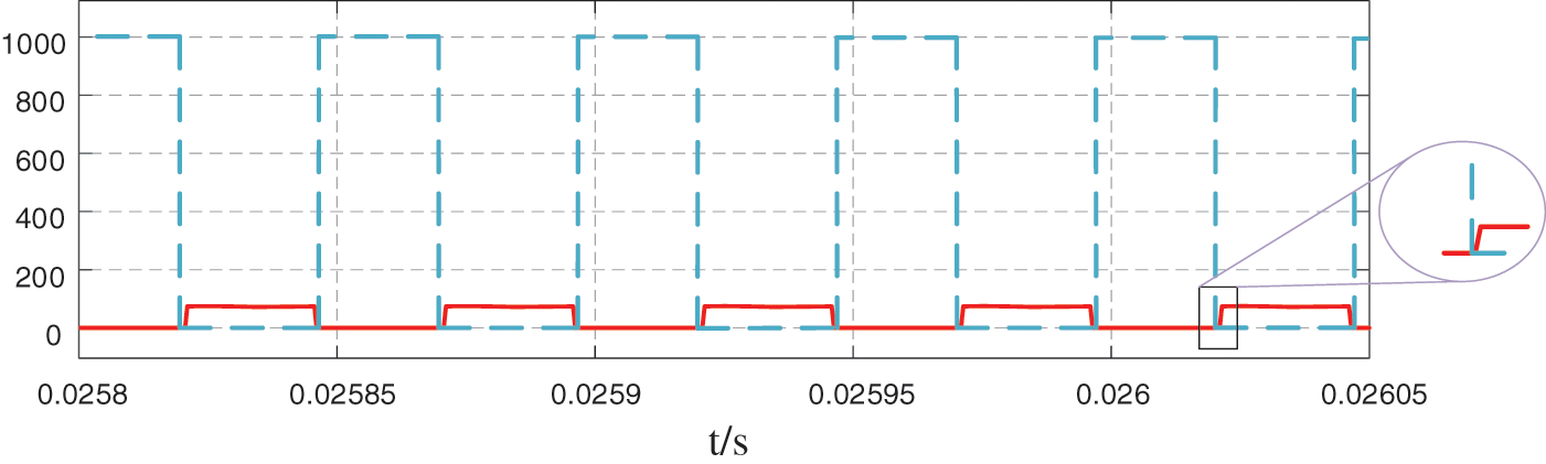
Figure 13: The soft switching function of switching S1
We have conducted experiments for further verification. In this paper, a hardware prototype is built, integrating the control circuit and the phase-shifted full-bridge module and the drive signal, as shown in Fig. 14. The relevant parameters are listed in Table 3, and the input magnitude is changed by adjusting the amplitude with a DC input instead of a PV power input.
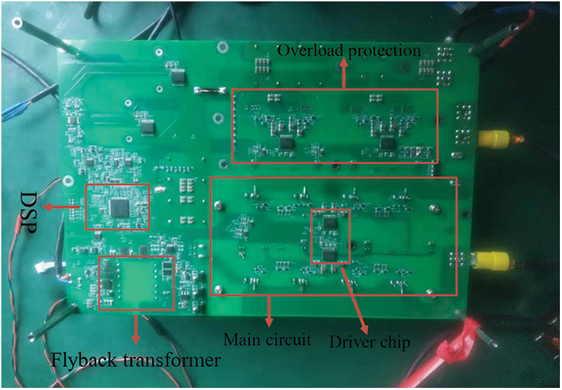
Figure 14: Experimental hardware platform
Fig. 15 shows the waveforms of
Figure 15: Experimental waveforms of
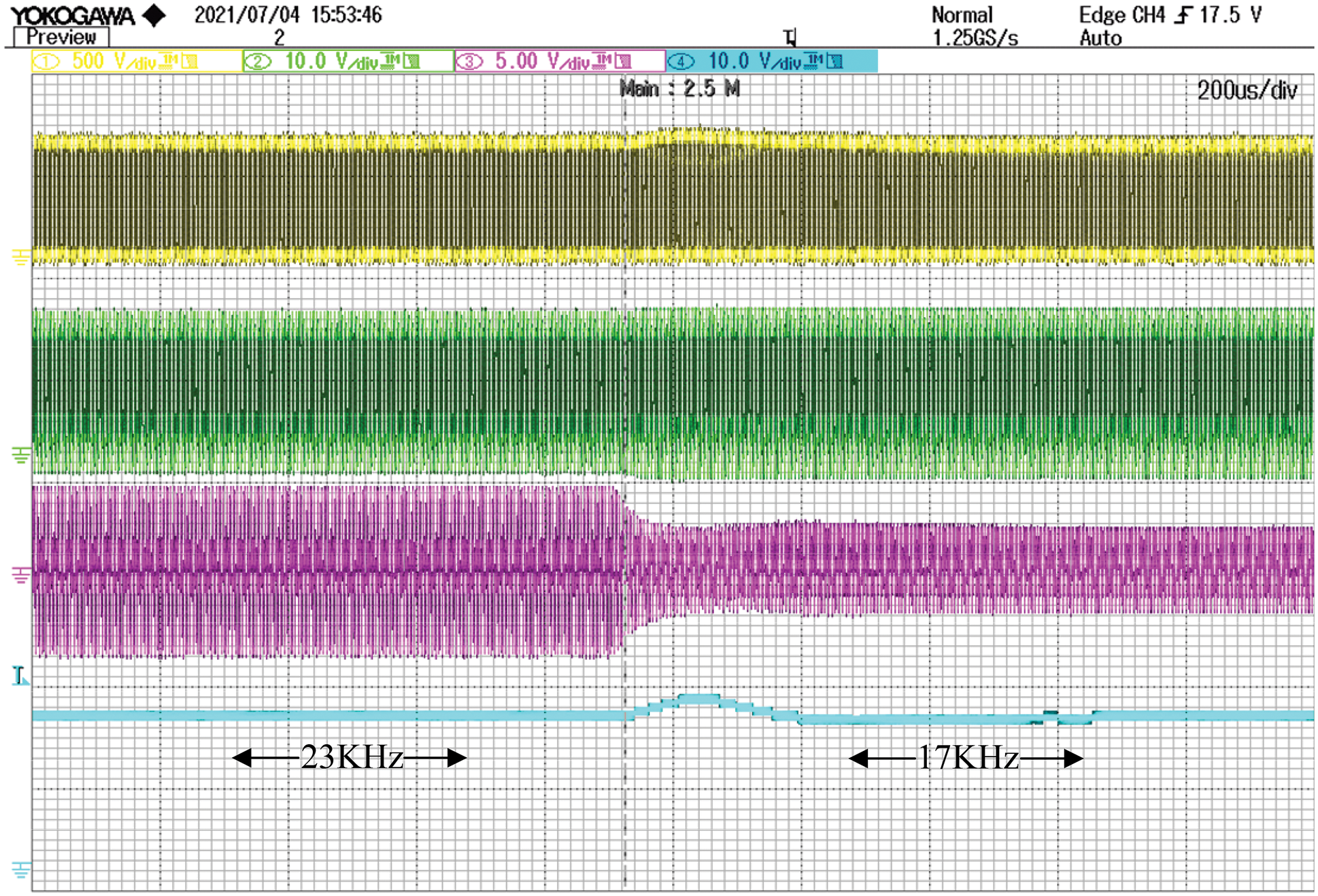
Figure 16: Experimental amplified waveforms of
The waveforms of

Figure 17: Experimental waveforms of
Fig. 18 shows the waveforms of
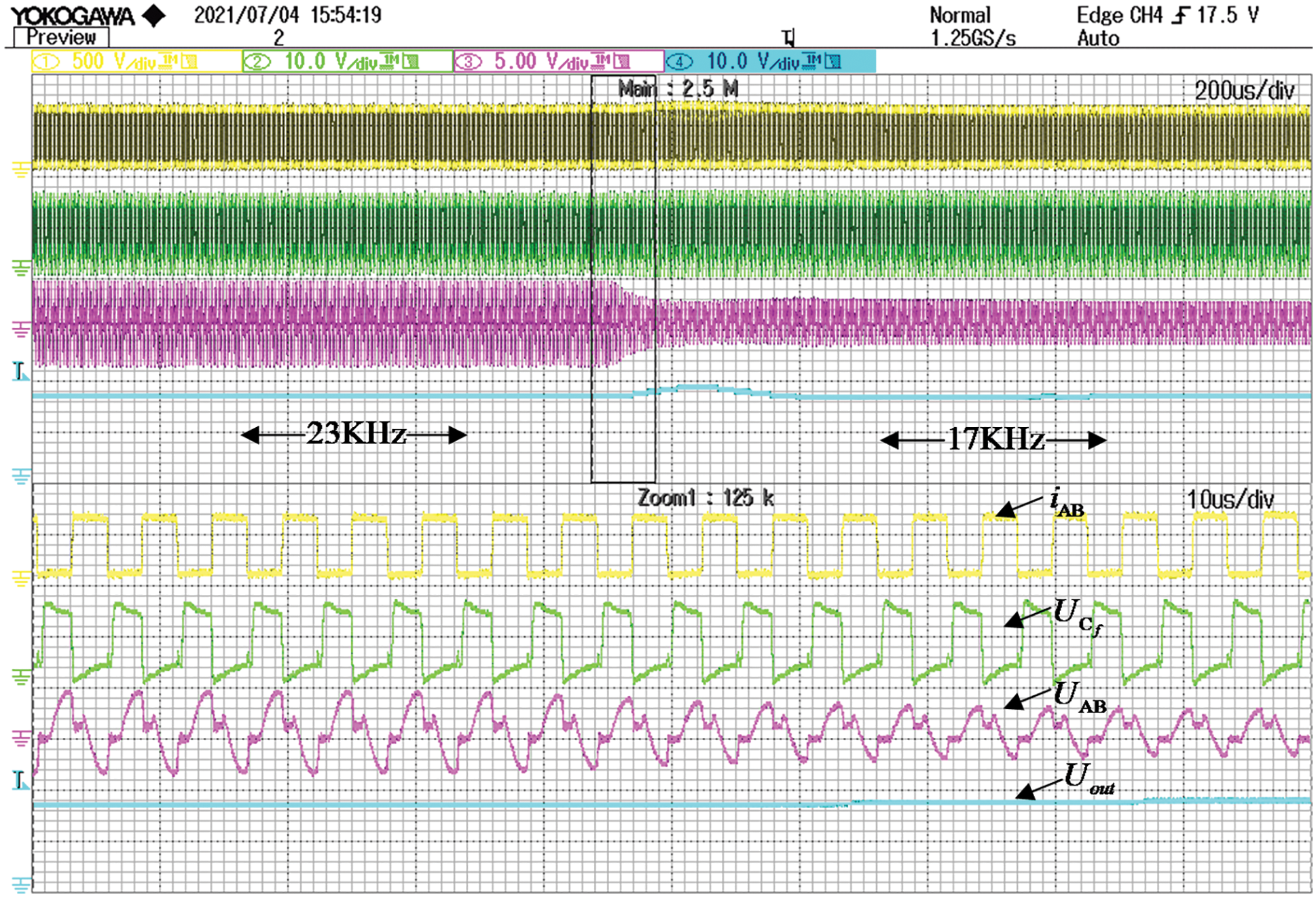
Figure 18: Experimental waveforms of
Fig. 19 shows the voltage and current through switch S1 during S1 startup. The yellow line represents the voltage, and the green line represents the current. It can be seen from the figure that during startup, when the voltage drops, the current rises very slowly, as it is facilitated by the resonant commutation between
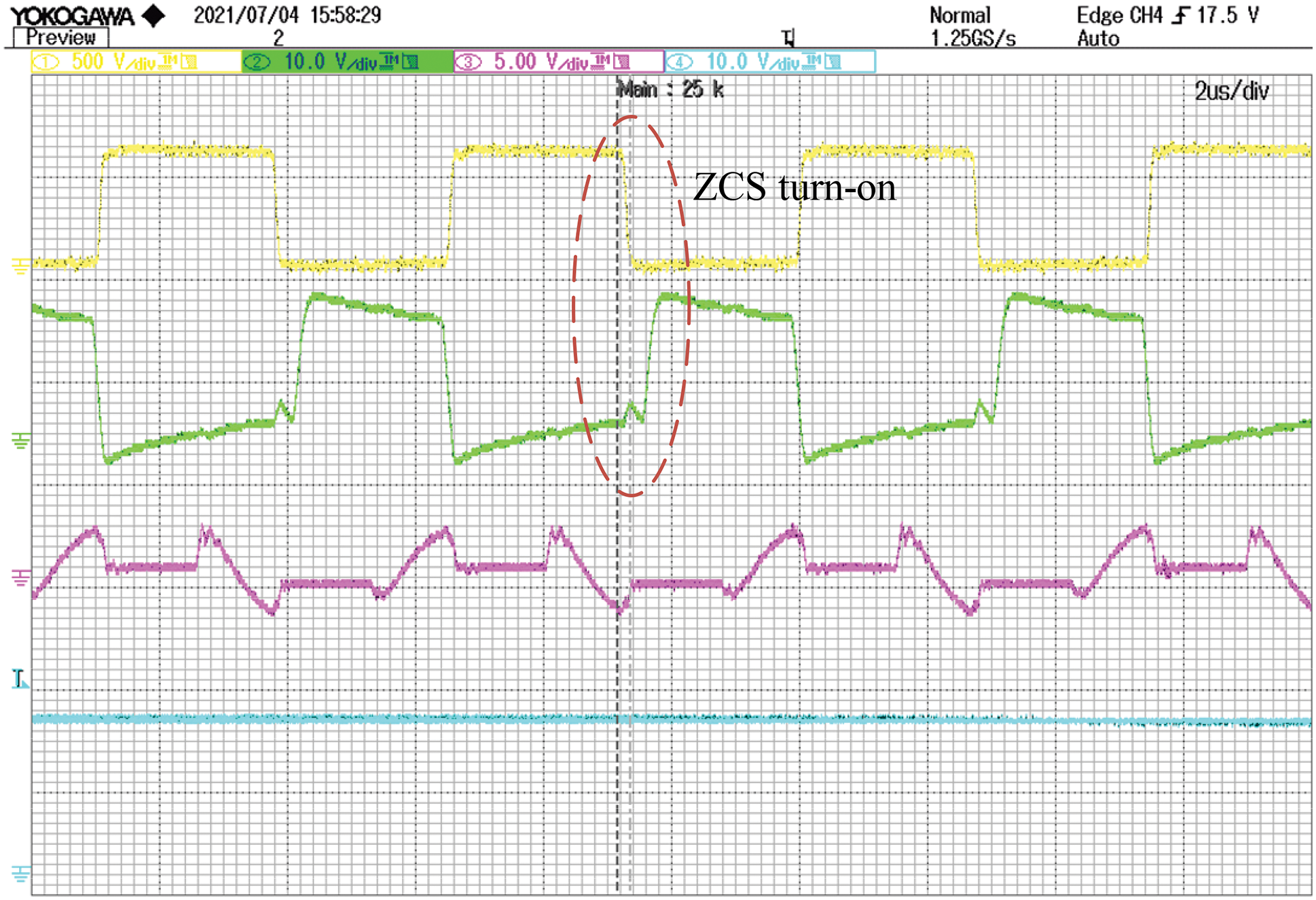
Figure 19: Experimental waveform of voltage and current of S1
A novel full-bridge zero-current converter (FB-ZCS) is designed, and a frequency and phase-shift synthesis modulation (FPSSM) control strategy is proposed. Automatic control of capacitor energy based on input current can be achieved without additional switches or auxiliary circuits by controlling the charging time of the capacitor. The control approach solves the problems of low efficiency and high duty cycle loss in the current commutation and soft-switching functions of existing full-bridge converters, which usually use transformer leakage inductance and parallel resonant capacitance. Finally, the theoretical analysis is first verified by simulation, and then an experimental hardware platform is built and further verified by experimentation. The conclusion shows that the novel converter designed by the FPSSM modulation technique has an excellent boosting effect and high reliability. The study shows that the method is simple in structure and has a good control effect. The module can be cascaded with IPOS and used in photovoltaic DC collection systems, providing a new topology scheme for large-scale, long-distance DC transmission.
Acknowledgement: The authors thank the support of the Tianjin University and Electric Power Research Institute of Yunnan Power Grid Co., Ltd.
Funding Statement: This work was supported by the Key R&D Program of Tianjin (No. 20YFYSGX00060).
Conflicts of Interest: The authors declare that they have no conflicts of interest to report regarding the present study.
1. Ajami, A., Ardi, H., Farakhor, A. (2015). A novel high step-up DC-DC converter based on integrating coupled inductor and switched-capacitor techniques for renewable energy applications. IEEE Transactions on Power Electronics, 30, 4255–4263. DOI 10.1109/TPEL.2014.2360495. [Google Scholar] [CrossRef]
2. Tran, D., Vu, H., Choi Woojin (2016). A novel quasi-resonant ZVZCS phase shift full bridge converter with an active clamp in the secondary. IEEE 8th International Power Electronics and Motion Control Conference, pp. 492–495. Hefei, China. [Google Scholar]
3. Li, Z., Wu, T., Zhang, G., Yang, R. (2018). Hybrid modulation method combining variable frequency and double phase-shift for a 10 kW LLC resonant converter. IET Power Electronics, 11, 2161–2169. DOI 10.1049/iet-pel.2018.5304. [Google Scholar] [CrossRef]
4. Ye, J., Yan, L., Pan, W., Luo, B., Zou, X. (2018). Generation of hybrid frequency and phase shift keying signal for radio over fiber system. Guangxue Xuebao/Acta Optica Sinica, 38, 80–84. DOI 10.3788/AOS201838.0206002. [Google Scholar] [CrossRef]
5. Edwin, F., Xiao, W., Khadkikar, V. (2014). Dynamic modeling and control of interleaved flyback module-integrated converter for PV power applications. IEEE Transactions on Industrial Electronics, 61, 1377–1388. DOI 10.1109/TIE.41. [Google Scholar] [CrossRef]
6. Sathyan, S., Suryawanshi, H. M., Ballal, M. S., Shitole, A. B. (2015). Soft-switching DC–DC converter for distributed energy sources with high step-up voltage capability. IEEE Transactions on Industrial Electronics, 62, 7039–7050. DOI 10.1109/TIE.2015.2448515. [Google Scholar] [CrossRef]
7. Shi, K., Zhang, D., Zhou, Z., Zhang, M., Zhang, D. et al. (2016). A novel phase-shift dual full-bridge converter with full soft-switching range and wide conversion range. IEEE Transactions on Power Electronics, 31, 7747–7760. DOI 10.1109/TPEL.2015.2512848. [Google Scholar] [CrossRef]
8. Zhao, L., Xu C, L., Zheng, X. (2018). A dual half-bridge phase-shifted converter with wide ZVZCS switching range. IEEE Transactions on Power Electronics, 33, 2976–2985. DOI 10.1109/TPEL.63. [Google Scholar] [CrossRef]
9. Azim, A. W., Le, Y., Ros, L. (2020). Hybrid frequency and phase-shift keying modulation for energy efficient optical wireless systems. IEEE Wireless Communications Letters, 9, 429–432. DOI 10.1109/LWC.5962382. [Google Scholar] [CrossRef]
10. Hiltunen, J., Vaisanen, V., Juntunen, R., Silventoinen, P. (2015). Variable-frequency phase shift modulation of a dual active bridge converter. IEEE Transactions on Power Electronics, 30, 7138–7148. DOI 10.1109/TPEL.2015.2390913. [Google Scholar] [CrossRef]
11. Hu, X., Gong, C. (2015). A high gain input-parallel output-series DC-DC converter with dual coupled inductors. IEEE Transactions on Power Electronics, 30, 1306–1317. DOI 10.1109/TPEL.2014.2315613. [Google Scholar] [CrossRef]
12. Li, T., Parsa, L. (2018). Design, control, and analysis of a fault-tolerant soft-switching DC–DC converter for high-power high-voltage applications. IEEE Transactions on Power Electronics, 33, 1094–1104. DOI 10.1109/TPEL.2017.2684832. [Google Scholar] [CrossRef]
13. N, G. Yadav, B., Narasamma N, L. (2014). An active soft switched phase-shifted full-bridge DC–DC converter: Analysis, modeling, design, and implementation. IEEE Transactions on Power Electronics, 29, 4538–4550. DOI 10.1109/TPEL.2013.2284780. [Google Scholar] [CrossRef]
14. U, P. K, R. Rathore, A. (2013). Extended range ZVS active-clamped current-fed full-bridge isolated DC-DC converter for fuel cell applications: Analysis, design, and experimental results. IEEE Transactions on Industrial Electronics, 60, 2661–2672. DOI 10.1109/TIE.2012.2194977. [Google Scholar] [CrossRef]
15. Sathyan, S., Suryawanshi, H., Shitole, A. (2014). Soft switched coupled inductor based high step up converter for distributed energy resources. 40th Annual Conference of the IEEE Industrial Electronics Society, pp. 1799–1805. Dallas, Texas, USA. [Google Scholar]
16. Pahlevaninezhad, M., Das, P., Drobnik, J., Jain, P., Bakhshai, A. (2012). A novel ZVZCS full-bridge DC-DC converter used for electric vehicles. IEEE Transactions on Power Electronics, 27, 2752–2769. DOI 10.1109/TPEL.2011.2178103. [Google Scholar] [CrossRef]
17. Fardoun, A., Ismail E, H. (2010). Ultra step-up DC–DC converter with reduced switch stress. IEEE Transactions on Industry Applications, 46, 2025–2034. DOI 10.1109/TIA.2010.2058833. [Google Scholar] [CrossRef]
18. Kim, E., Kwon, B. (2010). Zero-voltage-and zero-current-switching full-bridge converter with secondary resonance. IEEE Transactions on Industrial Electronics, 57, 1017–1025. DOI 10.1109/TIE.2009.2029581. [Google Scholar] [CrossRef]
19. Mousavi, A., Moschopoulos, G. (2014). A new ZCS-PWM full-bridge DC–DC converter with simple auxiliary circuits. IEEE Transactions on Power Electronics, 29, 1321–1330. DOI 10.1109/TPEL.2013.2259847. [Google Scholar] [CrossRef]
20. Xiao, H., Xie, S. (2008). A ZVS bidirectional DC–DC converter with phase-shift plus PWM control scheme. IEEE Transactions on Power Electronics, 23, 813–823. DOI 10.1109/TPEL.2007.915188. [Google Scholar] [CrossRef]
21. Yu, W., Lai, J., Lai, W., Wan, H. (2012). Hybrid resonant and PWM converter with high efficiency and full soft-switching range. IEEE Transactions on Power Electronics, 27, 4925–4933. DOI 10.1109/TPEL.2012.2192293. [Google Scholar] [CrossRef]
22. Mousavi, A., Das, P., Moschopoulos, G. (2012). A comparative study of a new ZCS DC–DC full-bridge boost converter with a ZVS active-clamp converter. IEEE Transactions on Power Electronics, 27, 1347–1358. DOI 10.1109/TPEL.2011.2118233. [Google Scholar] [CrossRef]
23. Zhou, S. L., Tian, Y. T., Bi, J. B. (2019). Research on phase-shifted full-bridge DC-DC converter based on FB-ZVZCS. Power Electronics, 53, 16–19. DOI CNKI:SUN:DLDZ.0.2019.12.005. [Google Scholar]
24. Li, W., Jiang, Q., Mei, Y., Li, C., Deng, Y. et al. (2015). Modular multilevel DC-DC converters with phase-shift control scheme for high-voltage DC-based systems. IEEE Transactions on Power Electronics, 30, 99–107. DOI 10.1109/TPEL.2014.2301722. [Google Scholar] [CrossRef]
25. Wang, H., Sun, Q., Chung, H., Tapuchi, S., Ioinovici, A. (2009). A ZCS current-fed full-bridge PWM converter with self-adaptable soft-switching snubber energy. IEEE Transactions on Power Electronics, 24, 1977–1991. DOI 10.1109/TPEL.2009.2018559. [Google Scholar] [CrossRef]
26. Kumar, M., Ashirvad, M., Babu, Y. N. (2017). An integrated Boost-Sepic-Ćuk DC–DC converter with high voltage ratio and reduced input current ripple, pp. 984–990. Chennai, Tamil Nadu, India: Elsevier, Ltd. [Google Scholar]
 | This work is licensed under a Creative Commons Attribution 4.0 International License, which permits unrestricted use, distribution, and reproduction in any medium, provided the original work is properly cited. |