| Energy Engineering |
DOI: 10.32604/ee.2022.018902
ARTICLE
An Insight into the Second-Harmonic Current Reduction Control Strategies in Two-Stage Converters
School of Electrical Engineering, Nantong University, Nantong, 226019, China
*Corresponding Author: Lei Zhang. Email: nttzzl@ntu.edu.cn
Received: 23 August 2021; Accepted: 18 October 2021
Abstract: Due to the components at twice the fundamental frequency of output voltage in the instantaneous output power of a two-stage single-phase inverter (TSI), the second harmonic current (SHC) is generated in the front-end dc-dc converter (FDC). To reduce the SHC, optimizing the control strategy of the FDC is an effective and costless approach. From the view of visual impedance, this paper conducts an intensive study on the SHC reduction strategies. Origin of the SHC is illustrated first. Then, the equivalent circuit models of the FDC under different control strategies are proposed to analyse the SHC propagation characteristic. The derived model can offer a better insight into how the inductor SHC is affected by the control parameters. According to the derived models, a synthesis of different control strategies is presented and the relevant parameters are listed for control design to achieve better suppression effect. The benefits and limitations of these control strategies are also discussed. Based on the proposed equivalent circuit models, several optimization methods are proposed to enhance the effect. A 1500 VA TSI prototype is built and simulated on MATLAB/Simulink, verifying the effectiveness of the proposed optimization methods. This paper is aimed to provide a guideline for the control design and control optimization of the TSIs.
Keywords: Two-stage single-phase inverter (TSI); second harmonic current (SHC); equivalent circuit models; optimization
Two-stage single-phase inverters (TSIs) have been widely used in renewable systems [1–4] such as distributed generation system and energy storage system. A typical structure of TSI is illustrated in Fig. 1. The front-end dc-dc converter (FDC) converts varying and/or mismatching input voltage to a specified voltage that is suitable for the desired ac output. The back-end dc-ac inverter realizes the inverter conversion to supply the output load.
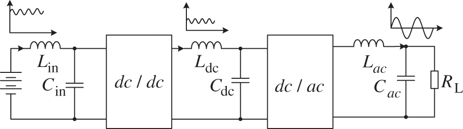
Figure 1: Typical configuration of a TSI
Due to the components at twice the fundamental frequency of output voltage in the instantaneous output power, the SHC is generated in the input current of the TSI. The SHC will increase the current stress and affect the lifetime of power switches. Moreover, the SHC causes extra power loss and lessen the soft-switching range of power switches, reducing the overall system efficiency [5]. Furthermore, if fuel cell is used to supply the two-stage inverter, the SHC will affect the fuel cell performance, cause extra fuel consumption and even shorten the life span [6,7]. Therefore, it is necessary to suppress the input SHC in the FDC. Two main methods are currently used to reduce the SHC in the FDCs: (1) Passive compensation methods (PCMs); (2) Active compensation methods (ACMs).
For an open-loop system, the magnitude of the SHC in the FDC is fully dependent on the passive energy-storage elements. Thus, the PCM is often to enlarge the energy storage elements in the converter (capacitor and/or inductor), such as connecting a large parallel capacitor to the input and/or the output terminals of the FDC [8] and connecting a LC series-resonance circuit in parallel with the output filter capacitor of the FDC [9]. However, for these cases, the cost will be increased and the size of the additional passive components may not be acceptable while the SHC is limited to the desired level [10].
As these disadvantages of the PCMs aforementioned, ACMs are more often used for their low cost and non-invasiveness. According to the different implementation approaches, the ACMs can be classified into two main categories. One way is the current-ripple injection method, where a bidirectional active filter is often used to compensate the required SHC of the dc-ac inverter [11–14]. However, with the additional bidirectional converter, the complexity of the system increases and more power loss is generated. The other way is the self-controlling method of the FDC, which is more commonly used for its convenience and low cost [15,16]. In this case, appropriate control approach is incorporated to force the intermediated inductor and/or capacitor to provide almost all the required second pulsating power. According to the different control purposes, the FDC self-controlling methods can be further divided into two types. One is the inductor SHC reduction strategy (FI-SHCRS) [5,17–22] and the other is the input SHC reduction strategy (I-SHCRS) [23,24]. However, there still is lack a unified model to describe the propagation mechanism of SHC and give an insight to all these control strategies for control optimization.
In order to analyse these methods from a unified perspective, equivalent circuit models of the FDC under different control strategies are proposed in this paper. The derived model can offer a better insight into how the inductor SHC is affected by the control parameters. According to the derived models, a synthesis of different control strategies is presented and the key parameters relevant to SHC are listed to reveal the benefits and limitations of these control strategies. Based on the proposed equivalent circuit models, several optimization methods are also proposed to enhance the effect. A 1500 VA TSI prototype is built and simulated on MATLAB/Simulink, verifying the effectiveness of the proposed optimization methods. This paper is aimed to provide a guideline for the control design and control optimization of the TSIs.
To study the composition of the input SHC, neglecting the switching harmonics, the downstream inverter is equivalent to a dc current source Idc in parallel with a SHC source i2nd, which is shown in Fig. 2.
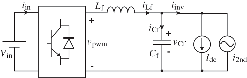
Figure 2: Equivalent model of a TSI
Lf and Cf are the filter inductor and the intermediate dc-bus capacitor respectively. vpwm, iLf, vCf, and iCf are the pulse width modulation (PWM) voltage, the inductor current, the intermediate bus voltage, and the current flowing through Cf, respectively. VCf is the dc component of vCf. When the switching frequency components are neglected, the instantaneous second harmonic power of the FDC can be given by
where vpwm_2nd, iLf_2nd, vCf_2nd, and iCf_2nd are the second harmonic components of vpwm, iLf, vCf, and iCf respectively. From Eq. (1), it can be seen that the pulsating power is divided into three parts: the part A is supplied by Vin; the part B is supplied by Lf; the part C is supplied by Cf. The part A is the root of the input SHC, which is composed of two items:
where vpwm_2nd depends on the pulsating component of the duty cycle d2nd. To reduce the input SHC, d2nd and iLf_2nd should be suppressed simultaneously.
In most applications, FI-SHCRS is sufficient to reduce the input SHC into an acceptable level and along with its easy implementation, is more commonly used. But for better suppression effect in particular applications, input SHC control strategy is needed.
3 Analysis of the Second Harmonic Current Propagation Characteristic
FI-SHCRS is the most common used method to suppress the input SHC of the two-stage inverters. For the FDC, control loops are often used to realize voltage regulation and short current limitation. Here, Buck converter is adopted as the FDC to analyse the influences of different control loop parameters on the SHC propagation. For a better insight into where the magnitude of the SHC lies, the equivalent circuit models under different control strategies are derived.
3.1 The Reverse Propagation Gains of SHC
Fig. 3 shows the control block diagrams of the FDC with open-loop, voltage single-loop, and voltage current dual-loop respectively, where Vm is the amplitude of the sawtooth carrier, Gv(s) is the voltage regulator, Gi(s) is the current regulator, Hv is the intermediate bus voltage sensor gain, and Hi is the inductor current sensor gain.
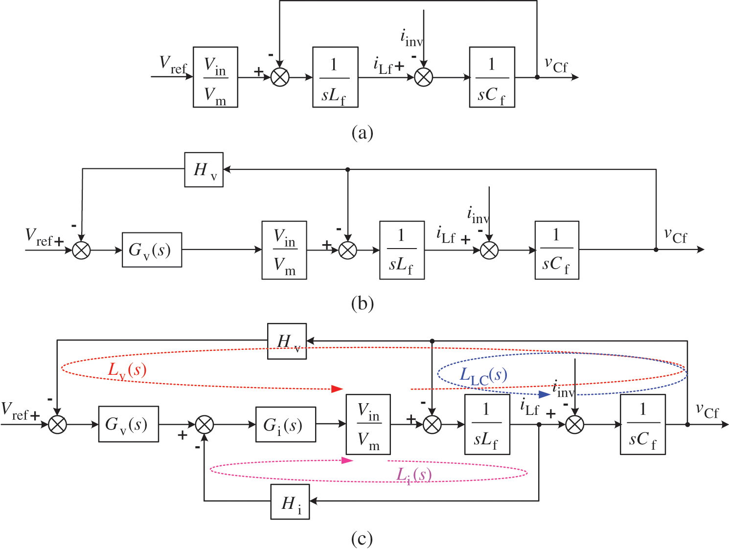
Figure 3: Control block diagrams of Buck converter under different control strategies: (a) Open-loop; (b) Voltage single-loop; (c) Voltage current dual-loop
According to Manson’s rule, the inductor second harmonic currents of the three control strategies can be derived respectively as
where Lv(s), Li(s), and LLC(s) are the gains of the outer voltage loop, the inner current loop, and LC filter loop as shown in Fig. 3c. The detailed expressions of these gains can be written as
From (5), it can be found that the introduction of the inner current loop increases its denominator and therefore decreases the inductor SHC. Actually, the numerator of (5) can also be decreased to reduce the inductor SHC. In [12], a load current feedforward branch with notch filter is introduced on the basis of the inner inductor current loop. Basically, this method is equal to adding an item to the numerator, which can be expressed by
where Gbpf(s) is the inserted notch filter. The added item decreases the amplitude of numerator at twice the output frequency, reducing the inductor SHC.
3.2 The Proposed Equivalent Circuit Models
The concept of visual impedance has been widely used in grid-connected inverters [25–28]. For two-stage single-phase inverters, visual-impedance-based control strategy is used to reduce SHC in [21] and to reveal the relationship among different SHC reduction schemes in [5,22]. Basically, visual-impedance is an intuitive comprehension of control loops. From this perspective, the original control loops can also be modelled as visual impedance. In this part, the effects of the control loops on the SHC propagation are analysed. In the following analysis, the voltage and current regulators both adopt proportional-integral (PI) controllers.
For the open-loop Buck converter, the equivalent circuit model can be derived according to Fig. 3a, as shown in Fig. 4. It can be found that in the case of open-loop control, the magnitude of the inductor SHC is fully dependent on the passive energy-storage elements (Lf and Cf). Thus, the passive compensation approach often enlarges the energy storage components [8,9]. To verify the correctness of the model, iLf0_2nd can be calculated again according to Fig. 4, which is given by
which is the same as (3).
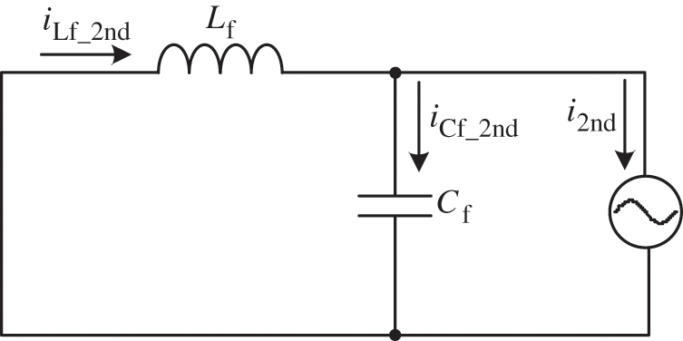
Figure 4: The equivalent circuit model of open-loop
For the voltage single-loop Buck converter, the equivalent control block diagram can be acquired by moving the voltage-loop feedback node as shown in Fig. 5a. Accordingly, the equivalent circuit model can be depicted as shown in Fig. 5b.
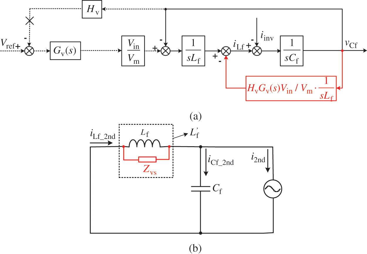
Figure 5: The equivalent circuit models of voltage single-loop: (a) Equivalent transform; (b) Equivalent circuit model
From this perspective, the voltage loop can be equivalent to a visual impedance Zvs(s) in parallel with the filter inductor, where 1/Zvs(s) can be expressed by
To verify the correctness of the model, iLf1_2nd can be calculated again according to Fig. 5b, which is given by
which is the same as (4). To analyse the effect of the voltage regulator parameters, we suppose Gv(s) as
Substituting (13) into (11) yields
It can be found that Zvs is composed of Zvs1 and Zvs2 in parallel. Zvs1 can be equivalent into a visual inductance and Zvs2 can be equivalent into a visual negative impedance whose value is proportional to s2. Whatever the type of impedance, both Zvs1 and Zvs2 decrease the impedance of the inductor branch, forcing the inductor to share more SHC. The larger of kpv and/or kiv are, the more SHC is distributed into the inductor branch.
For the voltage current dual-loop Buck converter, the equivalent transform 1 can be achieved by moving the voltage and current loop feedback nodes as Fig. 6a shows. Moreover, the feedback node of the voltage loop can be further moved as shown in Fig. 6b. Based on the transform 2, the equivalent circuit model can be derived as shown in Fig. 6c.
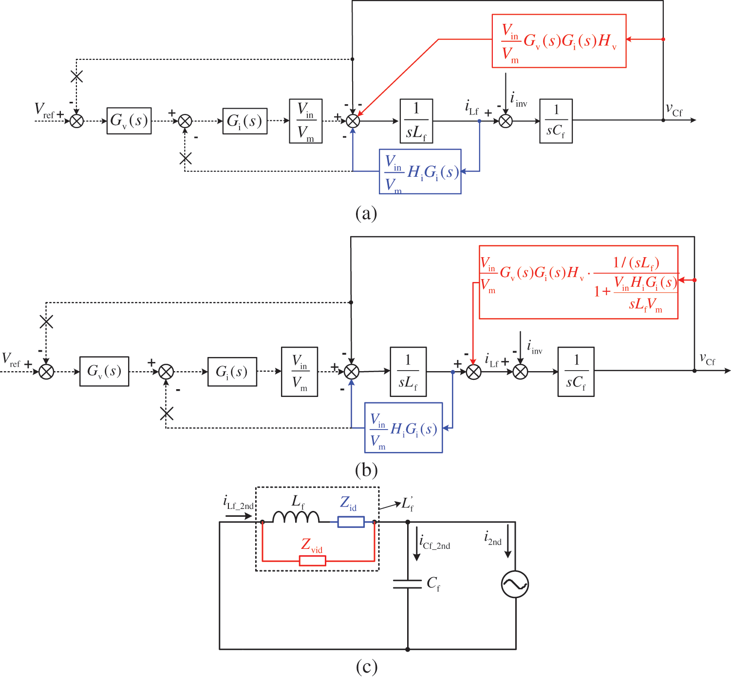
Figure 6: The equivalent circuit model of voltage current dual-loop: (a) Equivalent transform 1; (b) Equivalent transform 2; (c) Equivalent circuit model
From this perspective, the outer voltage loop is equivalent to a visual impedance Zvs(s) in parallel with the filter inductor and the inner current loop is equivalent to a visual impedance Zis(s) in series with the filter inductor, where 1/Zvid(s) and Zid(s) can be expressed respectively by
To verify the correctness of the model, iLf2_2nd can be calculated again according to Fig. 6c, which is given by
which is the same as (5). To analyse the effect of the voltage regulator parameters, we suppose Gv(s) the same as (13) and Gi(s) as
Substituting (13) and (18) into (15) yields
It can be found that Zvid is a series of Zvid1 and Zvid2, where Zvid1 is a parallel of three components [s/(kpvkpi), s2/(kpvkii+ kivkpi), s3/(kivkii)] and Zvid2 is a parallel of two components [Hi/( Hvkpv), His/( Hv kiv)]. Both Zvid1 and Zvid2 decrease the impedance of the inductor branch, forcing the inductor to share more SHC. The larger of kpv and/or kiv are, the more SHC is distributed into the inductor branch.
Substituting (18) into (16) yields
It can be found that Zid is a series of Zid1 and Zid2, where Zid1 is a visual resistance and Zid2 is a visual capacitance. Zid1 increases the impedance of the inductor branch, and the larger kpi is, the less SHC is distributed into the inductor branch. For Zid2, there is a serial resonance frequency of the visual capacitance and the filter inductance, which can be expressed by
Accordingly, the resonance frequency can be calculated by
In general, kii satisfies
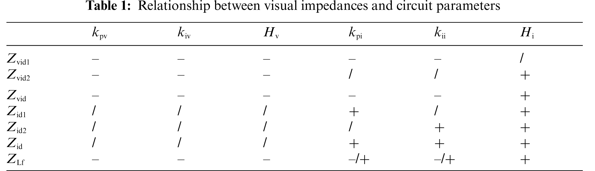
Therefore, Zid is usually proportional to kii. The relationships between the impedances of inductor branch and the circuit parameters are summarized in Table 1.
In conclusion, the impedance of the inductor branch ZLf can be increased by decreasing kpv, kiv, Hv and/or increasing Hi. In order to reduce the inductor SHC, the amplitudes of kpv, kiv, and Hv at twice the output frequency should be decreased and/or the amplitude of Hi at twice fundamental frequency of output voltage should be increased. Moreover, the amplitude of Hi at twice fundamental frequency of output voltage is the best choice to be increased to reduce the SHC because it can increase Zid(ω2nd) and Zvid(ω2nd) simultaneously. In general, these parameters should be selected in according to the stability and the dynamic performance of the circuit. In order to avoid those negative influences, notch filters (band-pass filter or band-stop filter) are often used.
3.3 The Relationship between the Inductor SHC and the Input SHC
The visual impedance is useful for the analysis of the inductor SHC but may be helpless for the analysis of the input SHC. Fig. 6c cannot be equivalent to the circuit model described in [22], which is shown in Fig. 7a. According to Fig. 7a, the input SHC can be completely eliminated by reducing the inductor SHC completely. However, apparently, it cannot be achieved according to (2).
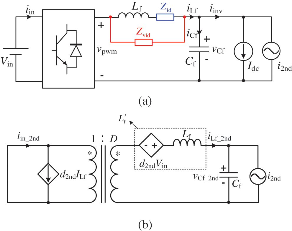
Figure 7: Second harmonic equivalent circuit model of the Buck converter: (a) Non-equivalent circuit model [22]; (b) AC equivalent circuit model
Actually, if the dc components and the harmonic components at the switching frequency are neglected, a Buck converter is equivalent to the circuit model as shown in Fig. 7b.
As a matter of fact, the equivalent inductor Lf' is a synthesis of the two items as shown in the dotted box of Fig. 7, and essentially the visual impedance is regulated by d2nd. No matter how Lf' is adjusted, d2nd undergoes corresponding change. In some cases, although Lf' is adjusted to a high value, the input SHC still keeps an observable value due to the d2nd.
4 Discussion and Optimization of SHC Reduction Strategies
The existing SHC reduction control strategies are reviewed and an insight into the existing inductor SHC reduction strategies from the visual impedance is provided.
In [17] and [18], an inner inductor current loop is introduced and the crossover frequency of the outer voltage loop is greatly reduced. Introducing the current loop is equivalent to inserting Zid(s) and reducing the crossover frequency of the outer voltage loop is equivalent to increasing Zvid(s) by decreasing kpv and kiv. By these means, the inductor SHC in the FDC can be reduced greatly. However, the low voltage loop crossover frequency will decrease the dynamic performance of the converter.
In [19], a notch filter (band-elimination filter) with the centre frequency at twice the output fundamental frequency is introduced into the output of the voltage loop (NF-VL), as shown in Fig. 8a. The introduced notch filter decreases the gain of the voltage regulator at twice the output fundamental frequency, which is equivalent to increasing Zvid(ω2nd) by decreasing kpv(ω2nd) and kiv(ω2nd). As a matter of fact, the notch filter Gbe(s) can be moved to the voltage feedback (NF-VF) as shown in Fig. 9a because Vref contains no second harmonic component. Meanwhile, to obtain a better effect, Zid(ω2nd) can be increased by inserting a band-pass filter with the centre frequency at twice the output fundamental frequency in parallel with current-loop regulator Gi(s) as shown in Fig. 9b (BPF-CLR).
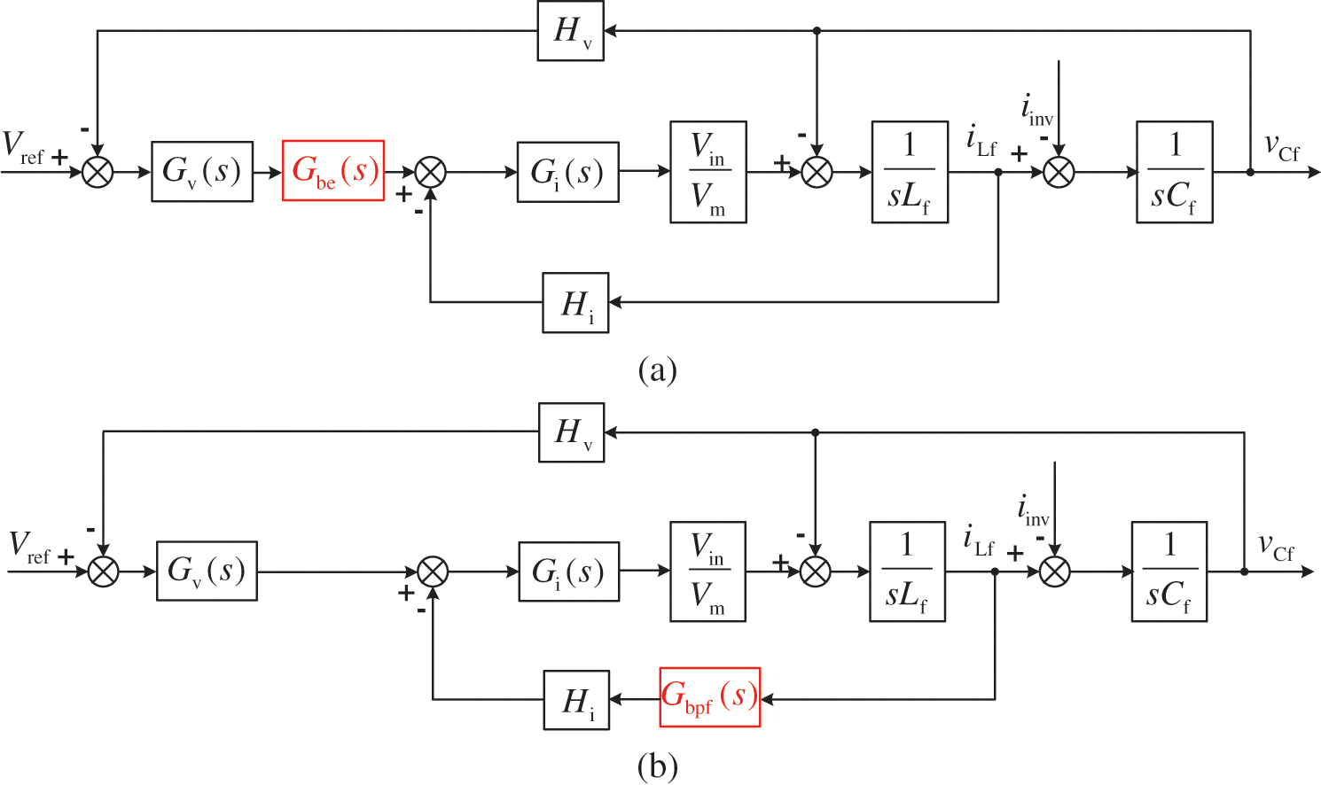
Figure 8: Control strategies for inductor SHC reduction: (a) NF-VL [18]; (b) BPF-CF [21]
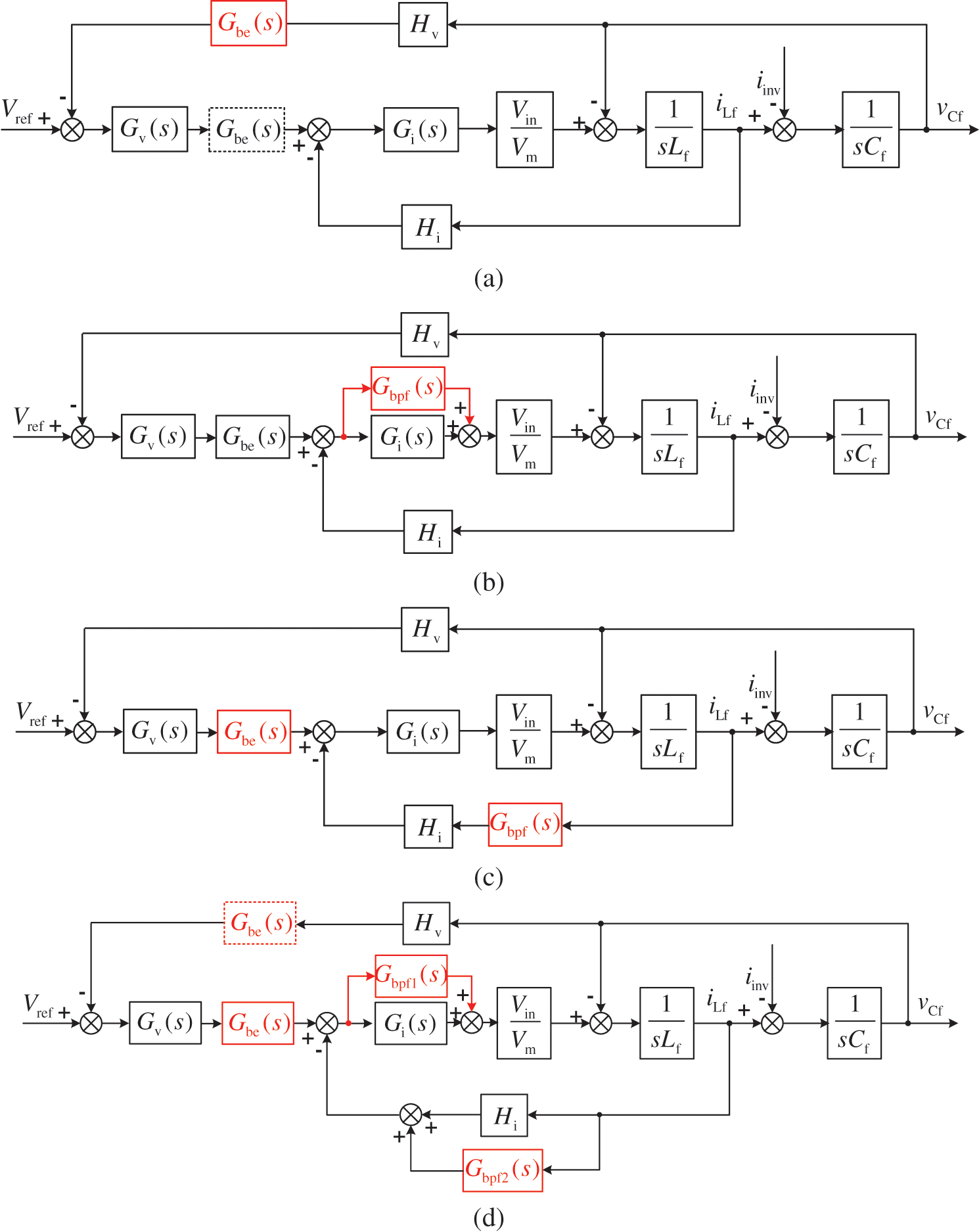
Figure 9: Available optimization strategies for inductor SHC reduction: (a) Optimization strategy 1; (b) Optimization strategy 2; (c) Optimization strategy 3; (d) A summary of available optimization strategies
In [21], a band-pass filter is incorporated to the inductor current feedback branch (BPF-CF), as shown in Fig. 8b. The introduced band-pass filter increases the gain of the inner current loop at twice the output frequency, equivalent to increasing Zid(ω2nd) and Zvid(ω2nd) by increasing Hi(ω2nd). In fact, the control schemes in [19] and [21] can be combined as shown in Fig. 9c to obtain a better effect.
Actually, for a voltage current dual-loop Buck converter, these control strategies can be summarized as shown in Fig. 9d. A notch filter or any combination of each of these notch filters (band-pass or band-elimination filters) in Fig. 9d can be used for the inductor SHC reduction.
In [20], a load current feedforward branch with notch filter (band-pass filter) is introduced on the basis of the inner inductor current loop. The introduced branch decreases the numerator of (9) and thus the inductor SHC is reduced. In combination with the control scheme in [19], this method is optimized in [20].
In [22], the relationship among different control schemes is revealed from the perspective of the output impedance of the FDC. However, it is important to note that no matter how the visual impedance in series with Lf and/or in parallel with Lf change, d2nd undergoes a corresponding change. The difference between Figs. 7a and 7b should be noted.
In order to achieve a better effect in the input SHC reduction, the input SHC is directly extracted for control [23]. However, the inductor current is often used for loop control. To avoid the use of the extra input current sensor, vriLf is used for the extraction of the input SHC, where vr is the modulation signal [24].
In order to verify the analysis above, a 1500 VA TSI prototype is built and simulated on MATLAB/Simulink. The FDC is a push-pull forward converter, and the downstream inverter is a single-phase full-bridge inverter. The main parameters of the built TSI are listed in Table 2.
5.1 The Reverse Propagation Gains of SHC
The reverse propagation gains of SHC are drawn as shown in Fig. 10, which verifies the analysis from the view of visual impedance and the proposed equivalent models.
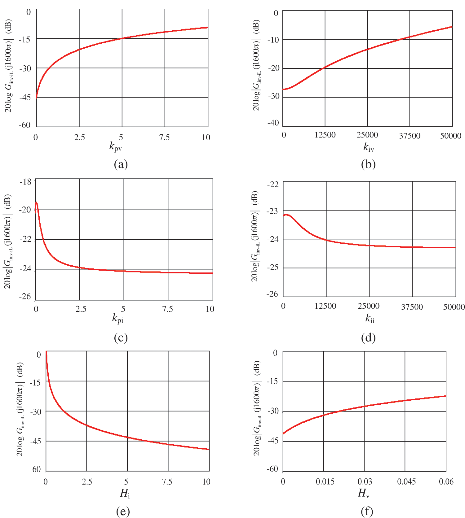
Figure 10: The reverse propagation gains of SHC: (a) kpv; (b) kiv; (c) kpi; (d) kii; (e) Hv; (f) Hi
5.2 Results of Different Control Loops
Fig. 11 shows the steady-state inductor current under open loop, single voltage closed-loop, voltage and current double closed-loop respectively from top to bottom, where kpv = 1.1, kiv = 100, and kpi = 1, kii = 1000. It can be seen that the introduction of the current loop reduces the inductor SHC effectively.
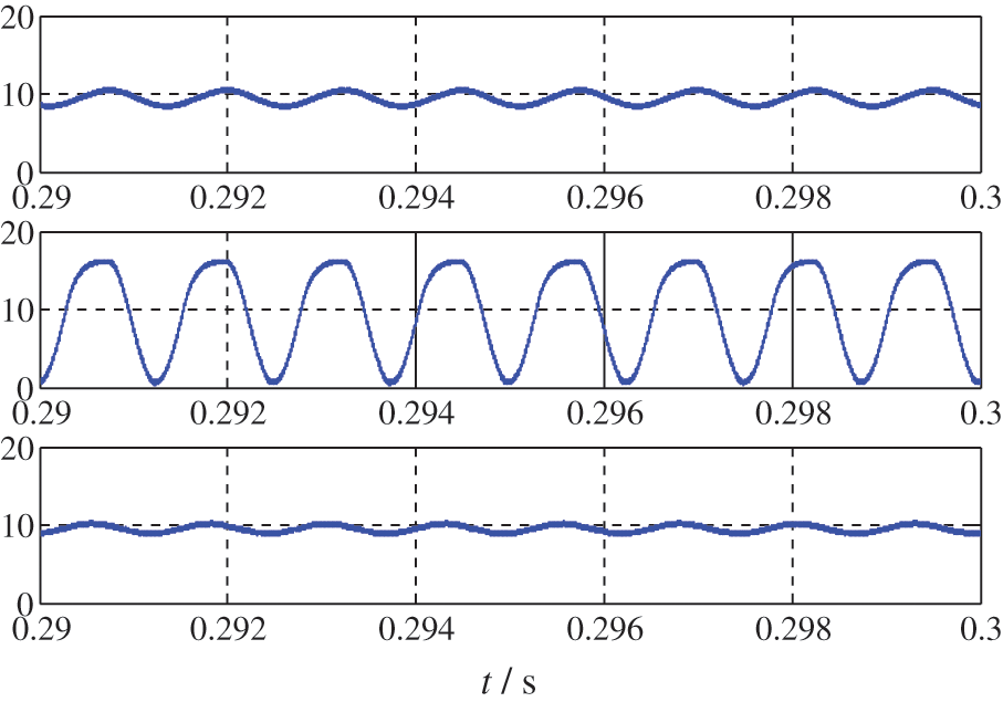
Figure 11: Simulation waveforms of inductor current with different control loops
Fig. 12 shows the steady-state inductor current under different loop parameters, where kpi is changed in Fig. 12a and kii is changed in Fig. 12b. From Fig. 12a, it can be seen that the suppression effect can be improved by increasing kpi in a certain range, which agrees well with Fig. 10c. From Fig. 12b, it can be seen the suppression effect is insensitive to kii, which agrees well with Fig. 10d.
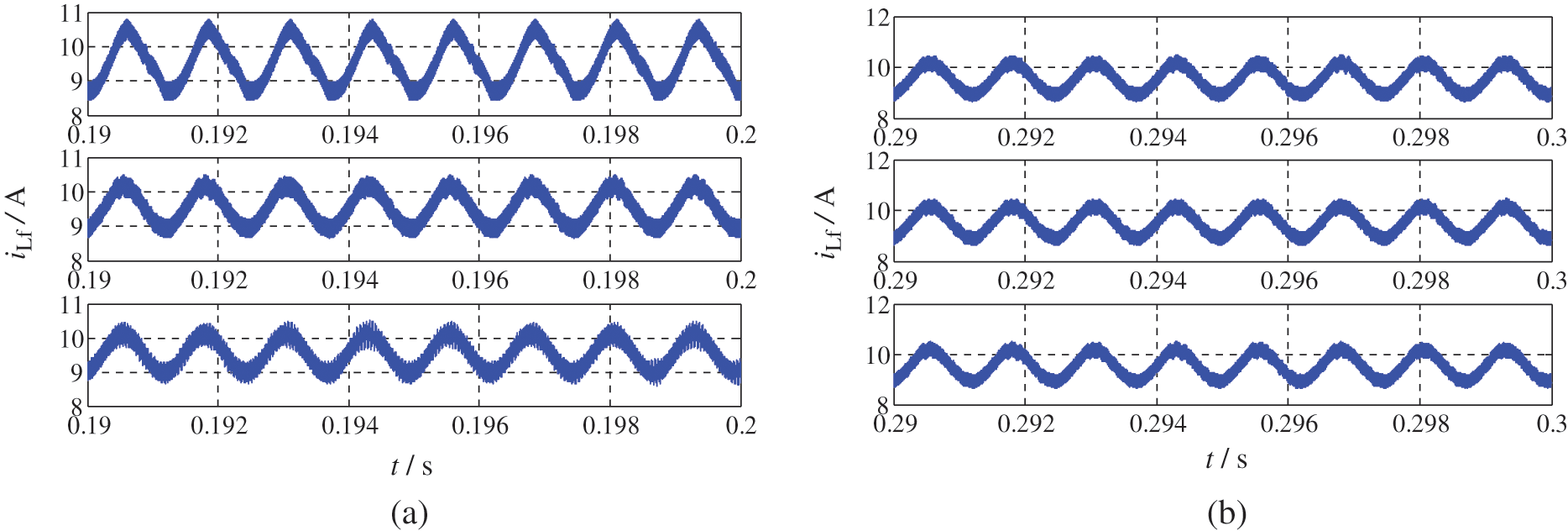
Figure 12: Simulation waveforms of inductor current with different loop parameters: (a) kpv = 1.1, kiv = 100, kii = 1000, and kpi = 0.1, 1, 10 from top to bottom; (b) kpv = 1.1, kiv = 100, kpi = 1, and kii = 0.1, 10, 1000 from top to bottom
5.3 Results of Optimization Strategies
Fig. 13 shows the steady-state inductor current under different control strategies and Fig. 14 shows the corresponding fast Fourier transform spectrums. From Fig. 13a, it can be seen that NF-VL is equivalent to NF-VF. From Figs. 13b and 14b, it can be seen that the optimization strategy 2 can achieve better suppression effect than NF-VL. From Figs. 13c and 14d, it can be seen that the suppression effect of BPF-CF is greatly improved by the optimization strategy 3. Obliviously, the simulation results verify correctness of the theory analysis and the effectiveness of the optimization strategies.
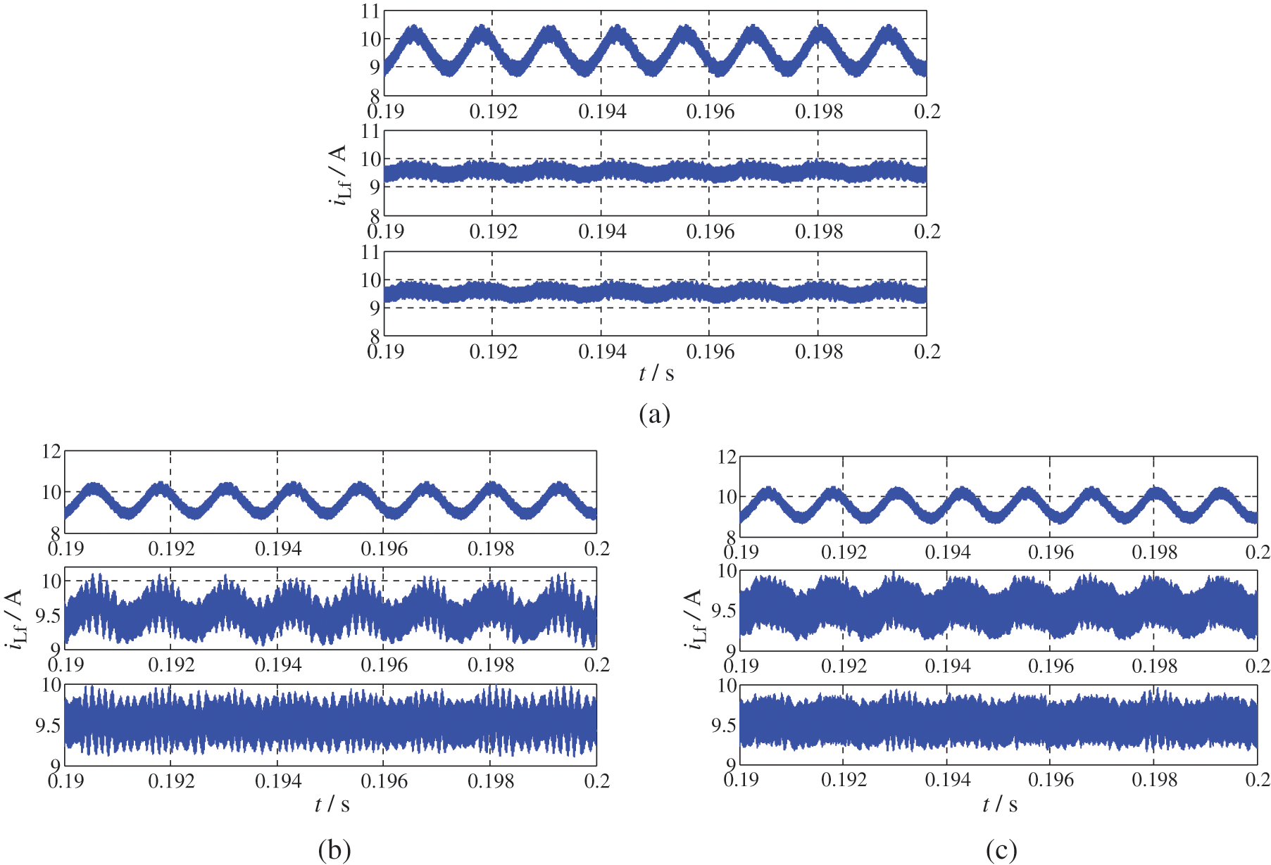
Figure 13: Simulation waveforms of inductor current: (a) Optimization strategy 1: without SHC reduction, NF-VL, NF-VF; (b) Optimization strategy 2: without SHC reduction, NF-VL, NF-VL+ BPF-CLR; (c) Optimization strategy 3: without SHC reduction, BPF-CF, BPF-CF + NF-VL
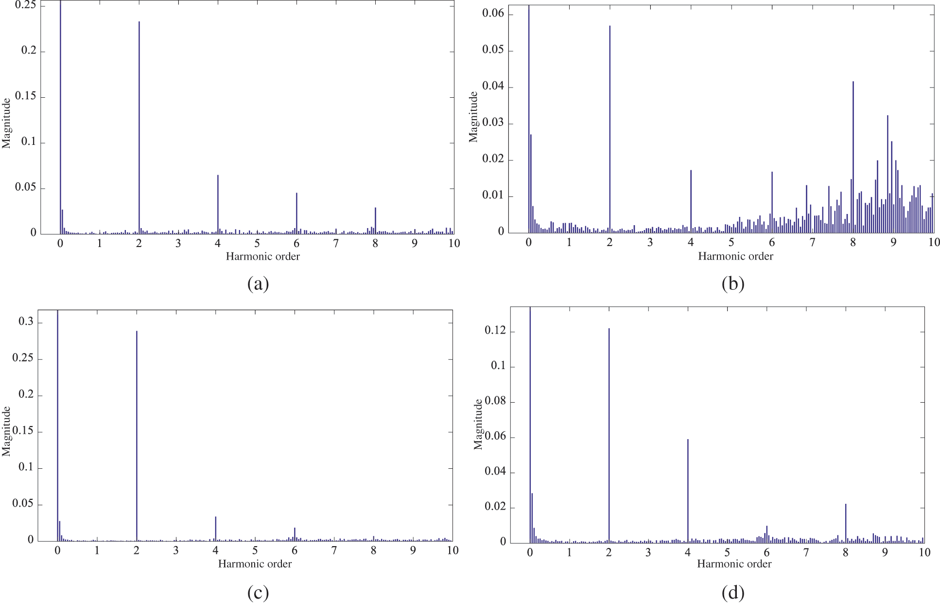
Figure 14: The fast Fourier transform spectrums: (a) NF-VL; (b) NF-VL + BPF-CLR; (c) BPF-CF; (d) BPF-CF + NF-VL
Due to the components at twice the output voltage frequency in the instantaneous output power of a two-stage single-phase inverter, the second harmonic current (SHC) is generated in the front-end dc-dc converter. To reduce the SHC, optimizing the control strategy of the front-end dc-dc converter is an effective and costless approach. According to the input pulsating instantaneous power analysis, the origin of the input SHC is divided into two parts: d2nd and iLf_2nd. According to the different purposes of control, the front-end dc-dc converter self-controlling methods are divided into two types. One is the inductor SHC reduction strategy (FI-SHCRS) and the other is the input SHC reduction strategy (I-SHCRS).
For a better comprehension of FI-SHCRS, equivalent circuit models are proposed from the view of visual impedance. The derived models can offer a better insight into where the magnitude of the inductor SHC lies when the front-end dc-dc converter is under different control strategies. Meanwhile, important parameters, which can be used to reduce the inductor SHC, are analysed and summarized. Knowledge about the effects of these parameters on the SHC propagation can serve as a guideline for the design and optimization of the front-end dc-dc converters.
With the derived circuit models, different inductor SHC reduction schemes are reviewed and several optimization strategies are proposed. The limitation of FI-SHCRS is also revealed and I-SHCRS is indicated to be a better control strategy in the input SHC reduction.
Funding Statement: This work was supported in part by the Natural Science Foundation of Jiangsu Province under Grant BK20200969 (L.Z., http://std.jiangsu.gov.cn/).
Conflicts of Interest: The authors declare that they have no conflicts of interest to report regarding the present study.
1. Xue, Y., Chang, L., Kjaer, S. B., Bordonau, J., Shimizu, T. (2004). Topologies of single-phase inverters for small distributed power generators: An overview. IEEE Transactions on Power Electronics, 19(5), 1305–1314. DOI 10.1109/TPEL.2004.833460. [Google Scholar] [CrossRef]
2. Dong, D., Cvetkovic, I., Boroyevich, D., Zhang, W., Wang, R. et al. (2013). Grid-interface bidirectional converter for residential DC distribution systems—Part one: High-density two-stage topology. IEEE Transactions on Power Electronics, 28(4), 1655–1666. DOI 10.1109/TPEL.2012.2212462. [Google Scholar] [CrossRef]
3. Wang, W., Liu, B., Hu, Y., Li, Z., Wang, H. et al. (2021). Power decoupling control for single-phase grid-tied PEMFC systems with virtual-vector-based MPC. IEEE Access, 9, 55132–55143. DOI 10.1109/ACCESS.2021.3071776. [Google Scholar] [CrossRef]
4. Pardhi, P. K., Sharma, S. K., Chandra, A. (2020). Control of single-phase solar photovoltaic supply system. IEEE Transactions on Industry Applications, 56(6), 7132–7144. DOI 10.1109/TIA.2020.3024171. [Google Scholar] [CrossRef]
5. Zhang, L., Ruan, X. (2019). Control schemes for reducing second harmonic current in two-stage single-phase converter: An overview from dc-bus port-impedance characteristics. IEEE Transactions on Power Electronics, 34(10), 10341–10358. DOI 10.1109/TPEL.2019.2894647. [Google Scholar] [CrossRef]
6. Lu, N., Yang, S., Tang, Y. (2017). Ripple current reduction for fuel-cell-powered single-phase uninterruptible power supplies. IEEE Transactions on Industrial Electronics, 64(8), 6670–6617. DOI 10.1109/TIE.2017.2677329. [Google Scholar] [CrossRef]
7. Sullivan, C., Awerbuch, J., Latham, A. (2013). Decrease in photovoltaic power output from ripple: Simple general calculation and the effect of partial shading. IEEE Transactions on Power Electronics, 28(2), 740–747. DOI 10.1109/TPEL.2012.2205162. [Google Scholar] [CrossRef]
8. Schenck, M., Stanton, K., Lai, J. S. (2005). Fuel cell and power conditioning system interactions. Proceedings of the 20th Annual IEEE Applied Power Electronics Conference and Exposition, pp. 6–10. Austin, USA. [Google Scholar]
9. Fukushima, K., Norigoe, I., Shoyama, M., Ninomiya, T., Harada, Y. et al. (2009). Input current-ripple consideration for the pulse-link dc-ac converter for fuel cells by small series LC circuit. Proceedings of the 24th IEEE Applied Power Electronics Conference and Exposition, pp. 15–19. Washington, USA. [Google Scholar]
10. Stevens, J. L., Shaffer, J. S., Vandenham, J. T. (2002). The service life of large aluminum electrolytic capacitors: Effects of construction and application. IEEE Transactions on Industry Applications, 38(5), 1441–1446. DOI 10.1109/TIA.2002.802922. [Google Scholar] [CrossRef]
11. Zhang, L., Ruan, X., Ren, X. (2018). One-cycle control for electrolytic capacitor-less second harmonic current compensator. IEEE Transactions on Power Electronics, 33(2), 1724–1739. DOI 10.1109/TPEL.2017.2682420. [Google Scholar] [CrossRef]
12. Huang, X., Ruan, X., Fang, J., Kan, S. (2021). A virtual impedance based control scheme for modular electrolytic capacitor-less second harmonic current compensator. IEEE Transactions on Industrial Electronics, 68(1), 198–209. DOI 10.1109/TIE.2019.2962402. [Google Scholar] [CrossRef]
13. Vitorino, M., Alves, L., Wang, R., Correa, M. (2017). Low-frequency power decoupling in single-phase applications: A comprehensive overview. IEEE Transactions on Power Electronics, 32(4), 2892–2912. DOI 10.1109/TPEL.2016.2579740. [Google Scholar] [CrossRef]
14. Sun, Y., Liu, Y., Su, M., Xiong, W., Yang, J. (2016). Review of active power decoupling topologies in single-phase systems. IEEE Transactions on Power Electronics, 31(7), 4778–4794. DOI 10.1109/TPEL.2015.2477882. [Google Scholar] [CrossRef]
15. Zhang, L., Ruan, X. (2019). Control schemes for reducing second harmonic current in two-stage single-phase converter: An overview from DC-bus port-impedance characteristics. IEEE Transactions on Power Electronics, 34(10), 10341–10358. DOI 10.1109/TPEL.2019.2894647. [Google Scholar] [CrossRef]
16. Zhang, L., Ruan, X. (2018). Second-harmonic current reduction for two-stage inverter with boost-derived front-end converter: Control schemes and design considerations. IEEE Transactions on Power Electronics, 33(7), 6361–6378. DOI 10.1109/TPEL.2017.2746878. [Google Scholar] [CrossRef]
17. Liu, C. R., Lai, J. S. (2007). Low frequency current ripple reduction technique with active control in a fuel cell power system with inverter load. IEEE Transactions on Power Electronics, 22(4), 1429–1436. DOI 10.1109/TPEL.2007.900594. [Google Scholar] [CrossRef]
18. Wang, J., Ji, B., Lu, X., Deng, X., Zhang, F. et al. (2014). Steady-state and dynamic input current low-frequency ripple evaluation and reduction in two-stage single-phase inverters with back current gain model. IEEE Transactions on Power Electronics, 29(8), 4247–4260. DOI 10.1109/TPEL.2013.2292609. [Google Scholar] [CrossRef]
19. Wei, Z., Deng, X., Gong, C., Chen, J., Zhang, F. (2012). A novel technique of low frequency input current ripple reduction in two-stage dc-ac inverter. Proceedings of the 38th Annual Conference on IEEE Industrial Electronics Society, pp. 25–28. Montreal, Canada. [Google Scholar]
20. Zhu, G., Ruan, X., Zhang, L., Wang, X. (2015). On the reduction of second harmonic current and improvement of dynamic response for two-stage single-phase inverter. IEEE Transactions on Power Electronics, 30(2), 1028–1041. DOI 10.1109/TPEL.2014.2307092. [Google Scholar] [CrossRef]
21. Zhang, L., Ren, X., Ruan, X. (2014). A bandpass filter incorporated into the inductor current feedback path for improving dynamic performance of the front-end dc-dc converter in two-stage inverter. IEEE Transactions on Industrial Electronics, 61(5), 2316–2325. DOI 10.1109/TIE.2013.2267704. [Google Scholar] [CrossRef]
22. Zhang, L., Ruan, X., Ren, X. (2015). Second-harmonic current reduction and dynamic performance improvement in the two-stage inverters: An output impedance perspective. IEEE Transactions on Industrial Electronics, 62(1), 394–404. DOI 10.1109/TIE.2014.2331015. [Google Scholar] [CrossRef]
23. Liu, X., Li, H., Wang, Z. (2014). A fuel cell power conditioning system with low-frequency ripple-free input current using a control-oriented power pulsation decoupling strategy. IEEE Transactions on Power Electronics, 29(1), 159–169. DOI 10.1109/TPEL.2013.2251004. [Google Scholar] [CrossRef]
24. Lei, R., Zhao, Y., Gong, C., Deng, X., Wei, Z. (2014). Analysis and suppression of the input second harmonic current in two-stage inverter. Proceedings of the 40th Annual Conference of the IEEE Industrial Electronics Society. Dallas, USA. [Google Scholar]
25. He, J., Li, Y. W. (2012). Generalized closed-loop control schemes with embedded virtual impedances for voltage source converters with LC or LCL filters. IEEE Transactions on Power Electronics, 27(4), 1850–1861. DOI 10.1109/TPEL.2011.2168427. [Google Scholar] [CrossRef]
26. Sun, J. (2011). Impedance-based stability criterion for grid-connected inverters. IEEE Transactions on Power Electronics, 26(11), 3075–3078. DOI 10.1109/TPEL.2011.2136439. [Google Scholar] [CrossRef]
27. Zhang, X., Ruan, X., Tse, C. K. (2015). Impedance-based local stability criterion for DC distributed power systems. IEEE Transactions on Circuits and Systems I: Regular Papers, 62(3), 916–925. DOI 10.1109/TCSI.2014.2373673. [Google Scholar] [CrossRef]
28. Zhang, Y., Yu, M., Liu, F., Kang, Y. (2013). Instantaneous current-sharing control strategy for parallel operation of ups modules using visual impedance. IEEE Transactions on Power Electronics, 28(1), 432–440. DOI 10.1109/TPEL.2012.2200108. [Google Scholar] [CrossRef]
 | This work is licensed under a Creative Commons Attribution 4.0 International License, which permits unrestricted use, distribution, and reproduction in any medium, provided the original work is properly cited. |