DOI:10.32604/iasc.2021.018903
| Intelligent Automation & Soft Computing DOI:10.32604/iasc.2021.018903 | |
| Article |
Hardware Acceleration of Image and Video Processing on Xilinx Zynq Platform
Department of Electronics and Communication Engineering, College of Engineering and Technology, SRM Institute of Science and Technology, Kattankulathur, 603203, India
*Corresponding Author: Eswaran Parthasarathy. Email: eswaranp@srmist.edu.in
Received: 25 March 2021; Accepted: 11 May 2021
Abstract: Advancements in image and video processing are growing over the years for industrial robots, autonomous vehicles, indexing databases, surveillance, medical imaging and computer-human interaction applications. One of the major challenges in real-time image and video processing is the execution of complex functions and high computational tasks. In this paper, the hardware acceleration of different filter algorithms for both image and video processing is implemented on Xilinx Zynq®-7000 System on-Chip (SoC) device. It consists of Dual-core Cortex™-A9 processors which provide computing ability to perform I/O and processing functions and software libraries using Vivado® High-Level Synthesis (HLS). In the proposed work, Sobel-Feldman filter, posterize and threshold filter algorithms are implemented for 1920 × 1080 image resolutions. The implementation results exhibit effective resource utilization such as 45.6% of logic cells, 51% of Look-up tables (LUTs), 29.47% of Flip-flops, 15% of Block RAMs and 23.63% of DSP slices under 100 MHz frequency on comparing with previous works.
Keywords: FPGAs; image and video processing; hardware acceleration; High-Level Synthesis; SoCs
Reconfigurable computing is a paradigm deals with the flexibility of high performance of hardware and software components that are processed using computing platforms such as Field-programmable gate arrays (FPGAs). With increasing popularity in reconfigurable computing [1], FPGAs are suitable for implementation of embedded hardware designs. FPGA offers a perfect base for image and video processing hardware structure mechanism, which provides performances similar to customized ICs. In association with emerging technology, image and video processing systems are widely used from space to security applications. Implementation of such algorithms on reconfigurable hardware increases performance, thereby accelerating standard algorithms that make the debug and verification processes simpler.
FPGA hardware architectures for image and video processing systems deliver support for applications like remote sensing, industrial reconnaissance, histopathology, medical diagnosis, television, photography, etc. The advanced developments in chip technology permit integrating extensive variety of functionalities on the host IC. Therefore, embedded SoC design engineers are involved with increased design prerequisites like flexibility, power consumption, performance and cost. These arguing constraints affects the development time and cost. For this reason, there is a demand for flexible solutions which provides better accuracy while implementing and re-utilize after final implementation.
With the increasing improvements in technology, researchers are turned towards developing dedicated systems for image and video processing applications. Based on the emerging aspects such as reconfigurable systems, there are two stages for development. Firstly, software acceleration consisting of different instructions for the processor to enable the execution of various libraries for optimization. The second phase is the hardware implementation of such algorithms on the programmable logic offered by the devices. These integrations deliver the effective resource utilization, user-handling capability, real-time processing and many other advantages.
This paper is structured as follows. Background outline on hardware accelerators for both image and video processing systems are presented in Section II. Implementation of the development platform and filter algorithms are discussed in Section III. The hardware resource utilization and the overall performance of the proposed acceleration are summarized in Section IV and with concluding remarks in Section V.
There are numerous investigations are targeted at developing dedicated hardware accelerators to perform a particular process in image and video processing applications. The video processing development system is demonstrated by implementing some spatial filters on Zedboard embedded platform [2]. Another research about video processing hardware accelerator on Altera Cyclone IV FPGA with reduced computation and memory bandwidth requirement is explained [3]. The implementation of real-time image and video processing is designed with Platform Based Design (PBD) which explores the trade-off between different design requirements implemented on Virtex-5 FPGA [4]. PBD with efficient solution for architecture is implemented on Xilinx ML-507 platform, which captures real-time 640 × 480 VGA resolution video frames at 60 fps [5]. The different types of designs using Histogram of Oriented Gradients (HOG) algorithm for processing resolution of 1920 × 1080 pixels achieving 39.6 fps implemented on Xilinx Zynq® SoC [6]. The authors introduced OpenCV function for the hardware implementation on the ARM processor. The different types of hardware accelerated systems using FPGAs for image analysis are listed briefly in Cumplido et al. [7].
FPGAs are capable of performing multithreading operations that allow them to implement various applications, including automotive industries. Most researchers have demonstrated the development of image and video processing in driver assistance systems (DA) [8]. Claus et al. [9] presented DA systems based on dynamic partial reconfiguration (DPR) for various driving circumstances to enhance security with Multi Processor System-on-Chip (MPSoC) architecture. With the benefits of DPR, they presented “Autovision” architecture for hardware accelerated engines. Several observations are focussed on advanced driver assistance systems for hardware implementations of real-time lane detection. Using Hough Transform, real-time lane detection is implemented using Vivado HLS tool at 100 MHz with 130 fps for 480 × 270 resolution on Xilinx Zynq-7000 platform [10].
FPGAs are well-suited for complex image and video processing applications such as K-means clustering, image segmentation and lossless compression [11]. Edge detection is a state-of-the-art image processing algorithm which is mostly adapted in surveillance systems. The hardware implementation for 4K video stream on Xilinx devices is discussed in Kowalczyk et al. [12]. FPGA based edge detection design is implemented for HD video streaming with rapid prototyping [13]. The analysis and investigation about edge detection filters based on FPGAs for real-time image and video processing algorithms are compared and explained [14]. The various classifications of FPGA architectures and their applications are discussed briefly in Babu et al. [15].
3 Acceleration of Proposed Architecture
The simplified block diagram for proposed system architecture is shown in Fig. 1. The design is applicable for both image and video processing as each pixel’s information is streamed successively. Nevertheless, for video processing, the algorithm may need either one or more pixels. It consists of various video processing operations that can be programmed by suitable algorithms and thereby accelerating particular filters implemented on the integrated blocks of the Xilinx SoC platform. The output is transmitted to a video processing component and display component directly. Furthermore, the processed output is generated and seen through HDMI monitor externally. Based on the design, different video processing accelerators in the programmable logic (PL) are implemented in Xilinx [16].
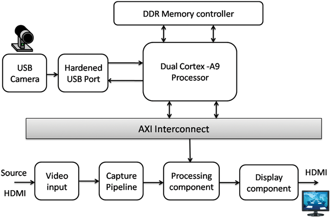
Figure 1: Simplified block diagram for proposed system architecture
There are two different types of architecture: one is direct streaming, and the other is frame buffer streaming. In direct streaming architecture, pixel information in the programmable logic can be sent to video processing component and transmitted to the output interface. However, in frame buffer streaming architecture, pixel information is saved in memory initially, and then video is processed with the required memory bandwidth. Based on the software and hardware acceleration, many image and video processing tasks are performed with the reconfigurable capability of Zynq SoCs. Along with software applications, embedded hardware filters and frame buffers built in the programmable logic section control the entire operating system. In this architecture, the video signals is transmitted to video processing pipeline through Advanced Extensible Interface (AXI) Interconnects from the processor. USB camera share the interfaces and communicate with the ARM processor. The image data is stored in the memory controller. Once the image is processed, it is sent through the output connected to HDMI display and pipeline is continued for the following iterations.
FPGAs gained quick acceptance over the past decades in the real-time image and video processing. FPGAs delivered better performance and are able to cut down design cost and exploit parallelism [17]. Compared with all other Xilinx FPGA families, Zynq-7000 APSoCs are stand-alone and unique. It is fabricated with integrating dual-core ARM Cortex-A9 Processing System (PS), Advanced Microcontroller Bus Architecture (AMBA) Interconnects, DDR3 component memory and several peripherals such as USB JTAG interface, CAN, UART, Ethernet and Quad SPI flash memory along with 7-series Xilinx Programmable Logic. Xilinx Zynq-7000 SoC XC7Z020-1CLG484C device is chosen as primary hardware for the proposed architecture to meet the design requirements is displayed in Fig. 2. FPGA is a reconfigurable platform that can allow the reuse of hardware components and software libraries.
The hardware modules provide more flexibility and parallelism towards computation than software modules. Due to hardware acceleration, real-time video stream is achieved based on design considerations and interface requirements. AXI bus interconnections protocols are used to interconnect the hardware blocks with the processing system. The AXI4-Lite bus and AXI4 stream bus interface are used to access hardware registers and to broadcast data of input image from the IP cores to frame buffers placed inside DDR3 component memory. AXI4 stream block is also used to convert the input data into the AXI4 stream interface. The video timing controller generates video signals for the test pattern generator within the FPGA.
It if followed by the video frames received from VDMA and transferred to the memory controller. The output is received from the external HDMI interface.
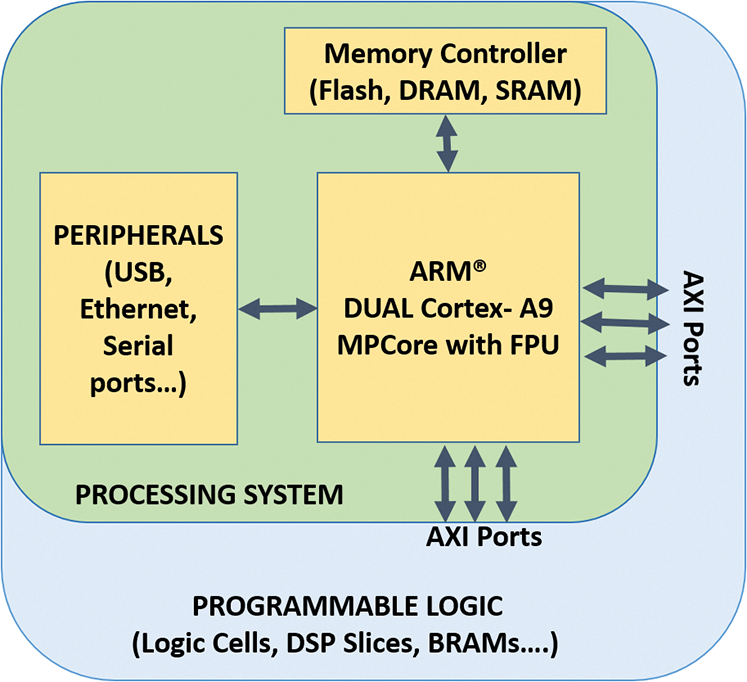
Figure 2: Overview of Xilinx Zynq-7000 SoC XC7Z020-1CLG484C device
The filter algorithms is implemented on dual-core ARM Cortex-A9 PS. It is feasible to implement various spatial filters for real time image and video processing while data is processed and stored in output memory simultaneously. The image filters used in this design are pipelined according to Sobel-Feldman filtering, posterize filtering and threshold filtering that are shown in Fig. 3. Sobel-Feldman filtering is a classical edge-detection algorithm in the real-time image and video processing [18], creating input data which emphasizes edges and transitions [19]. It represents x and y derivatives for the pixel values of an image. The core implements the Sobel-Feldman gradient based operator for convolution between Image (M) and two 3 × 3 kernels such as
The magnitude of gradient can be written as,
The gradient’s direction is given by,
Then Posterize filter is processed for conversion of tone gradation to input data from RGB format. Then it is followed by threshold filtering which converts high luminance pixels as white and low luminance pixels as black. For black pixel, the image intensity is
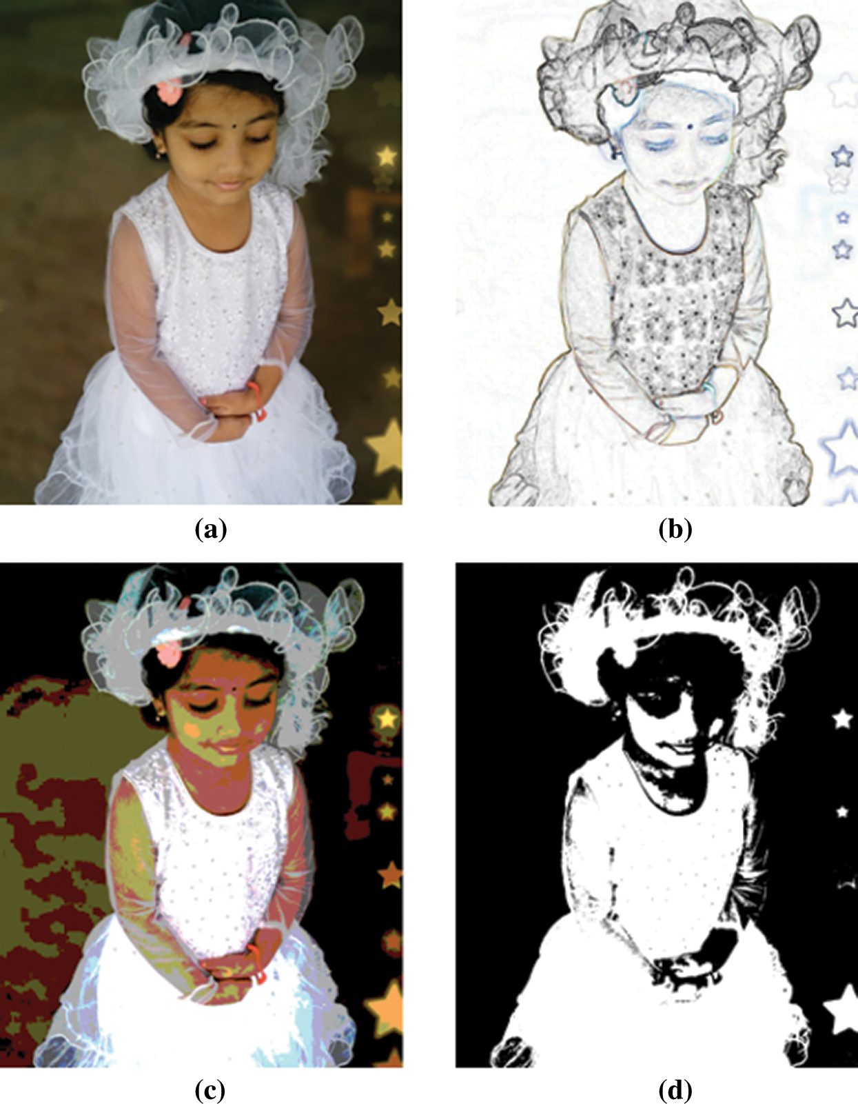
Figure 3: Results of different filtering techniques for 1920 × 1080 resolution input image (a) Input image. (b) Sobel-Feldman. (c) Posterize. (d) Threshold
IP core is configured with dimensions (width x height) of the input data. Once initializing IP core in the input interface, a video frame is accepted and processed. Then the processed frame is sent via the output interface. Simultaneously, the next video frame is received by the core which is ready to process without interruption and continued to process video frames. These processes will be extended until the total pipeline is processed and the image filter is stopped. The stream design uses a 4:2:2 YUV (16-bit) video format. However, 32-bit RGB controls the GUI layer of the display component.
Using Vivado HLS tool, C/C++ code is converted to RTL code for simulation. Vivado HLS has wide variety of library functions for video processing. Vivado HLS video libraries are implemented as synthesizable C/C++ code and equivalent to that of video processing functions implemented in OpenCV [20]. For example, cv::Mat class is the basic library used to represent 1920 × 1080 input resolutions in a video processing system is given by,
cv::Mat image (width, height, CV_8UC3);
hls::Mat <width, height, HLS_8UC3> image();
In order to find the size of the input image, Xilinx Video Timing Controller (VTC) is used. However, AXI4 stream interfaces expose the information through the output interface. The design flow involves in developing and generating an accelerator based on video library function for Application Program Interface (API) offered by Vivado HLS is shown in Fig. 4. API is used to recompile and execute the application. Some of the video library functions in Vivado HLS and OpenCV design flow are as follows.
• AXIvideo2Mat functions – convert AXI4 Streaming Video to hls::Mat representation
• Mat2AXIvideo functions – convert hls::Mat representation to AXI4 Streaming video stream
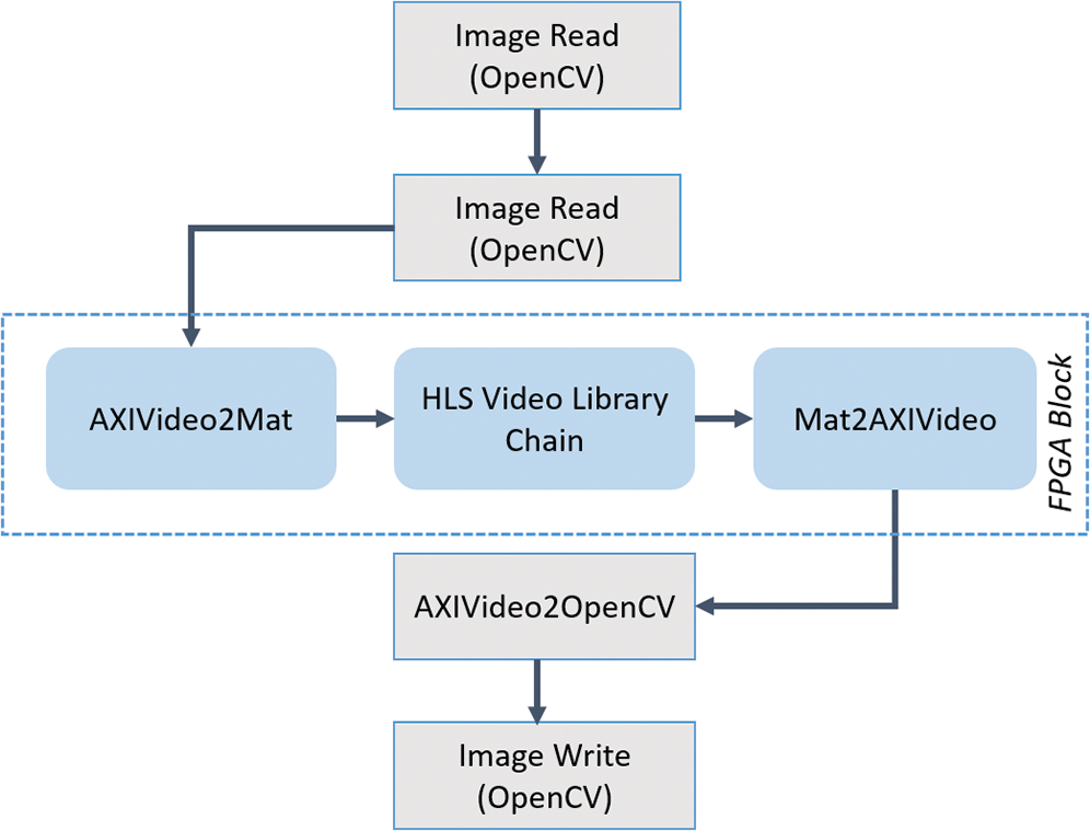
Figure 4: Vivado HLS video libraries design flow
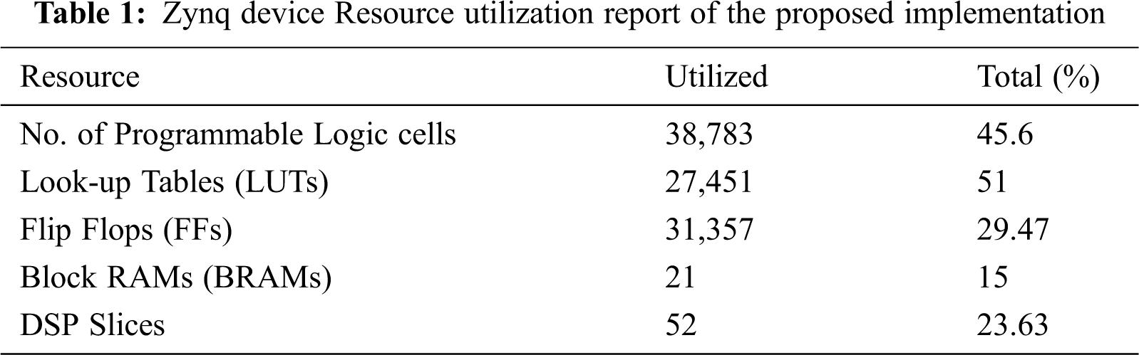
The entire processing system cores is implemented on Zynq 7000 SoC XC7Z020-CLG-484-1 [21]. The synthesis and implementation of the entire system is achieved at an optimum frequency at approximately 100 MHz. Some of the physical constraints such as exhaustion of DSP blocks is noticed while analyzing the performance and flexibility. The resources of SoC chip utilized for the designs may vary depending on the complexity of the implemented design. The three different types of filter designs are performed for the input resolution of 1920 × 1080 images. Tab. 1 report shows resource utilization summary for the implemented system. The results prove the advantages of using Vivado HLS tool on the reconfigurable SoC platform [22]. Almost 45% of total logic cells are utilized. The usage of the logic cells is varied according to placement and routing processes.
The resource utilization report for implementing filter algorithms compared with [2] and [13] is studied and are shown in Tab. 2. During the process, the implemented hardware accelerator system can produce video streams of the specific video processing algorithm. There is no communication exchange between FPGA and ARM processor which in turn prevent the communication overhead. The proposed model will achieve high performance to adapt various filtering techniques over the embedded processing platform.
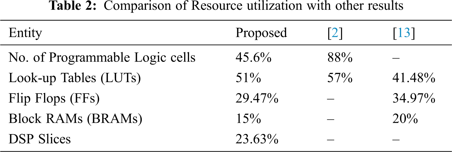
A hardware acceleration of three filter algorithms such as Sobel-Feldman filtering, posterize and threshold filtering for 1920 × 1080 image resolutions was implemented in Xilinx Zynq-7000 SoC hardware platform. Simulation and synthesis results were obtained using Vivado 2018.2. The resources utilization was studied and obtained as 45.6% of logic cells, 29.47% of flip-flops, 15% of BRAMs, 51% of LUTs and 23.63% of DSP blocks. From the simulation results, the proposed algorithm implementation utilized 40% and 29% less number of logic cells and LUTs respectively [2] in addition to 10% and 3% less number of flip-flops and BRAMs respectively [13]. In the proposed design, filter algorithms are processed simultaneously which provides flexibility and parallelism for hardware accelerators. Furthermore, the future exploration is focused on implementing these filter algorithms on dedicated reconfigurable hardware system for deep learning applications.
Acknowledgement: We would like to thank SRM Institute of Science and Technology for providing facilities to carry out the research work.
Funding Statement: The authors received no specific funding for this study.
Conflicts of Interest: The authors declare that they have no conflicts of interest to report regarding the present study.
1. I. Page, “Reconfigurable processor architectures,” Microprocessors and Microsystems, vol. 20, no. 3, pp. 185–196, 1996. [Google Scholar]
2. J. C. Mora, E. C. Gallego and S. S. Solano, “Hardware/software co-design of video processing applications on a reconfigurable platform,” in Int. Conf. on Industrial Technology (ICITSeville, Spain: IEEE, pp. 1694–1699, 2015. [Google Scholar]
3. K. F. Kong Wong, V. Yap and T. P. Chiong, “Hardware accelerator implementation on FPGA for video processing,” in IEEE Conf. on Open Systems (ICOSKuching, Malaysia, pp. 47–51, 2013. [Google Scholar]
4. L. Kechiche, L. Touil and B. Ouni, “Real-time image and video processing: Method and architecture,” in 2nd Int. Conf. on Advanced Technologies for Signal and Image Processing (ATSIPIEEE, Monastir, Tunisia, pp. 194–199, 2016. [Google Scholar]
5. J. G. Pandey, A. Karmakar and S. Gurunarayanan, “Architectures and algorithms for image and video processing using FPGA-based platform,” in 18th Int. Sym. on VLSI Design and Test (VDATIEEE, pp. 1, 2014. [Google Scholar]
6. J. Rettkowski, A. Boutros and D. Göhringer, “HW/SW co-design of the HOG algorithm on a Xilinx Zynq SoC,” Journal of Parallel and Distributed Computing, vol. 109, pp. 50–62, 2017. [Google Scholar]
7. R. Cumplido, M. Gokhale and M. Huebner, “Guest Editorial: Special issue on Reconfigurable Computing and FPGA technology,” Journal of Parallel and Distributed Computing, vol. 133, pp. 359–361, 2019. [Google Scholar]
8. K. Vipin and S. A. Fahmy, “FPGA dynamic and partial reconfiguration: A survey of architectures, methods, and applications,” ACM Computing Surveys, vol. 51, no. 4, pp. 1–39, 2018. [Google Scholar]
9. C. Claus, W. Stechele and A. Herkersdorf, “Autovision – A run-time reconfigurable MPSoC architecture for future driver assistance systems,” IT- Information Technology, vol. 49, no. 3, pp. 181–187, 2007. [Google Scholar]
10. C. Khongprasongsiri, P. Kumhom, W. Suwansantisuk, T. Chotikawanid, S. Chumpol et al., “A hardware implementation for real-time lane detection using high-level synthesis,” in International Workshop on Advanced Image Technology (IWAIT), Chiang Mai, Thailand: IEEE, pp. 1–4,2018. [Google Scholar]
11. D. G. Bailey, “Image processing using FPGAs,” Journal of Imaging, vol. 5, no. 53, pp. 1–4, 2019. [Google Scholar]
12. M. Kowalczyk, D. Przewlocka and T. Krvjak, “Real-time implementation of contextual image processing operations for 4K video stream in Zynq UltraScale+ MPSoC,” in Conf. on Design and Architectures for Signal and Image Processing (DASIPPorto, Portugal, pp. 37–42, 2018. [Google Scholar]
13. A. B. Amara, E. Pissaloux and M. Atri, “Sobel edge detection system design and integration on an FPGA based HD video streaming architecture,” in 11th Int. Design & Test Sym. (IDTHammamet, Tunisia, pp. 160–164, 2016. [Google Scholar]
14. E. Onat, “FPGA implementation of real time video signal processing using Sobel, Robert, Prewitt and Laplacian filters,” in 25th Signal Processing and Communications Applications Conf. (SIUAntalya, Turkey, pp. 1–4, 2017. [Google Scholar]
15. P. Babu and E. Parthasarathy, “Reconfigurable FPGA architectures: A survey and applications,” Journal of the Institution of Engineers (IndiaSeries B (Springer), vol. 102, pp. 143–156, 2021. [Google Scholar]
16. Xilinx Inc, Partial reconfiguration of a hardware hccelerator with Vivado Design Suite for Zynq-7000 APSoC processor. XAPP1231 (v1.1). [Online]. Available: https://www.xilinx.com/support/documentation/application_notes/xapp1159-partial-reconfig-hw-accelerator-zynq-7000.pdf. [Google Scholar]
17. M. A. V. Rodriguez, J. M. S. Pkrez and J. A. G. Pulido, “Recent advances in computer vision and image processing using reconfigurable hardware,” Microprocessors and Microsystems, vol. 29, no. 8–9, pp. 359–362, 2005. [Google Scholar]
18. S. Eetha, S. Agrawal and S. Neelam, “Zynq FPGA based system design for video surveillance with Sobel edge detection,” in 2018 IEEE Int. Sym. on Smart Electronic Systems (iSES) (Formerly iNiSHyderabad, India, pp. 76–79, 2018. [Google Scholar]
19. Xilinx Inc, Zynq All Programmable SoC Sobel filter implementation using the Vivado HLS tool. [Online]. Available: https://www.xilinx.com/support/documentation/application_notes/xapp890-zynq-sobel-vivado-hls.pdf. [Google Scholar]
20. Xilinx Inc, Accelerating OpenCV applications with Zynq-7000 All Programmable SoC using Vivado HLS video libraries. [Online]. Available: https://www.xilinx.com/support/documentation/application_notes/xapp1167.pdf. [Google Scholar]
21. Xilinx Inc, Zynq SoC overview datasheet. [Online]. Available: https://www.xilinx.com/support/documentation/data_sheets/ds190-Zynq-7000-Overview.pdf. [Google Scholar]
22. Xilinx Inc, “Vivado Design Suite tutorial high level synthesis, UG871 (v 2014.1) May 6, 2014,” UG871 (v 2014.1) May 6, 2014. [Online]. Available at: https://www.xilinx.com/support/documentation/sw_manuals/xilinx2019_1/ug871-vivado-high-level-synthesis-tutorial.pdf. [Google Scholar]
 | This work is licensed under a Creative Commons Attribution 4.0 International License, which permits unrestricted use, distribution, and reproduction in any medium, provided the original work is properly cited. |