DOI:10.32604/iasc.2022.020216
| Intelligent Automation & Soft Computing DOI:10.32604/iasc.2022.020216 | |
| Article |
Design and Analysis of a Novel Antenna for THz Wireless Communication
1Department of Electrical Engineering, Engineering Faculty, The Hashemite University, Zarqa, 13133, Jordan
2Communications Engineering Department, Princess Sumayya University for Technology, Amman, 11941, Jordan
3Department of Allied Engineering Sciences, Engineering Faculty, The Hashemite University, Zarqa, 13133, Jordan
*Corresponding Author: Omar A. Saraereh. Email: eloas2@hu.edu.jo
Received: 14 May 2021; Accepted: 15 June 2021
Abstract: The frequency range of the terahertz (THz) band is usually defined as 0.3~3.0 THz, and some scholars have also extended it to 0.1~10 THz. THz technology has the characteristics of low photon radiation energy and rich spectrum information, and the THz band contains the vibration and rotation resonance frequencies of many material macromolecules, which can realize fingerprint detection. Therefore, THz technology has great academic value and a wide range of applications in basic research and applied science. Application prospects, such as THz spectroscopy technology provides a new means for studying the interaction between electromagnetic waves and matter, and its application in sensing has also penetrated into semiconductors, biology and medicine and health, homeland security, food quality control and environmental testing and other major fields. This paper proposes a novel patch antenna structure for the THz communication. The proposed antenna is designed on a polyimide substrate and graphene. The prominent feature of this antenna is that the radiation performance is does not deteriorates when tuning the frequency points. The frequency is controlled through a bias electrical field and not the conventional electronic switch. Theoretical analysis is performed for frequency-tuning and the equivalent circuit model is utilized to determine the input impedance. Simulation results show that the proposed THz antenna operates in the wideband THz with high gain and radiation efficiency.
Keywords: THz antenna; metamaterial; microstrip patch; smart antenna
For a long time, the development maturity of THz technology is far behind the microwave and infrared bands on both sides of this band. People call this phenomenon the THz gap. The reason is that the technology used to generate and detect THz radiation is relatively immature, and there is still a lack of stable, efficient, and compact THz radiation sources under room temperature working conditions, especially 0.5 to 2.0 THz, an extremely important band in THz applications [1–3]. THz is located in the middle of the microwave and infrared bands in the electromagnetic spectrum, and has certain characteristics of microwave and light waves. Therefore, the generation of THz radiation can start from both the electronics technology based on the microwave band and the photonics technology based on the infrared band. Although higher power THz radiation can be generated based on vacuum electronics or plasma electronics technology, most of these radiation sources have limitations, such as only generating low-frequency THz waves with a narrow bandwidth and requiring large electron accelerators (such as free electrons) [4,5]. Laser or synchrotron radiation source), it is difficult to adapt to the needs of THz research in ordinary laboratories. Although the frequency of the electronic signal can be gradually amplified from low frequency to high frequency by using a multi-stage amplifier, its output power will drop rapidly as the frequency increases, such as the products of Virginia Diodes Inc. At present, high-frequency (greater than 1.0 THz) or broadband THz radiation is mainly achieved through optical-based methods [6,7].
There are many principles for generating THz radiation based on optical methods, and the representative ones are photoconductive effect and nonlinear optical difference frequency [8,9]. The photoconductivity effect is that the pump light with photon energy greater than the semiconductor forbidden band width is incident on the semiconductor to generate electron-hole pairs. These carriers generate a photo-generated current under the action of an external direct current (DC) bias, and then radiate THz wave. However, the principle of generating THz radiation by nonlinear optical difference frequency is relatively simple, and only a material with a strong second-order nonlinear optical coefficient is needed. Since the femtosecond laser pulse appears as a function with Gaussian distribution in the frequency domain, when a femtosecond laser pulse with a larger power density is incident on a nonlinear material, optical fibers will pass through the nonlinear optical material between any two frequencies. The difference frequency effect eventually produces a THz radiation covering a wide frequency range, which appears as a pulse signal in the time domain. This process is also called the optical rectification effect, because its final effect is to extract the envelope of the femtosecond laser pulse, which is similar to the optical rectification phenomenon in second-order nonlinear optics. In order to improve the efficiency of THz radiation, it is usually necessary to match the propagation speed of femtosecond laser pulses in nonlinear materials (the group speed of the pump light) with the generated THz radiation. Dual-wavelength continuous-wave pump light can also produce continuous-wave THz radiation through the nonlinear difference frequency effect, but it is necessary for both lasers to have a large power density, so as to produce localities related to the frequency difference of the dual-wavelength laser in the nonlinear material. Polarization intensity of the domain. Using this polarization intensity as a THz radiation source can produce continuous wave THz radiation, the frequency of which can be adjusted simply by the frequency difference between the two lasers [10].
Terahertz communication has the advantages of large transmission capacity and good directionality. With the rapid development of terahertz sources and terahertz detectors, terahertz radiation has received more and more attention [11]. The application of terahertz bands in airborne communications, radio astronomy and other fields has greatly promoted the development of terahertz antenna research [12]. At the same time, the number of wireless communication devices is increasing rapidly, and higher requirements are placed on channel capacity. Based on frequency adjustable antennas, by tuning the frequency range, the antenna can maintain good radiation performance.
Graphene has excellent electrical, thermal and mechanical properties, and has received more and more attention in recent years [13,14]. Graphene has many advantages in terahertz antenna applications, such as miniaturization, mechanical flexibility and dynamic adjustability [15,16]. Various designs of antennas structures were proposed that are based on with metasurface planar feeding structure [17], leaky-wave slit dipole structure [18], multiple patch cells structure [19], WBAN-THz structure [20], synthesized photonic bandgap substrate using BPSO [21] and On-chip catadioptric THz lens antenna [22].
Affected by the heating effect and skin depth, metals have poor radiation performance and serious ohmic loss in the terahertz frequency band, while graphene has stable physical and mechanical properties, which can meet the needs of high-frequency performance [23,24]. In this paper, by designing an equivalent circuit model based on the graphene antenna, the relationship between the graphene characteristics and the antenna resonance frequency is found, and the relationship curve between the graphene chemical potential and the antenna resonance frequency is obtained, so as to obtain a more convenient method. To predict the radiation characteristics of the antenna. The antenna proposed in this paper has a simple structure, no parasitic elements and electronic devices, is not restricted by electrical switches and the feasible fabrication method at micro-manufacturing level which is deployed by literature [25–30] has been utilized. Compared with the previous research [31], the designed antenna has better performance in terms of gain, wide bandwidth and radiation efficiency.
2.1 Graphene Surface Conductivity
Graphene surface conductivity The surface conductivity of graphene plays an important role in the antenna frequency shift use.
Since the thickness of graphene is ultra-thin, it can be modeled by the surface conductivity σs.
When the lateral size of the structure is greater than 100 nm, the edge effect can be ignored. Therefore, when the voltage is biased, the surface conductivity of the graphene layer can be expressed by the Kubo formula [12–13] as
where ω = 2 πf is the angular frequency, f is the frequency; Γ is the scattering rate; μc is the chemical potential; T is the temperature; e is the electronic charge; h is the reduced Planck constant; ε is the energy; fd is the Fermi-Dirac distribution, which can be expressed as
In Eq. (2), kB is Boltzmann's constant. Usually, room temperature (T = 300K) is selected, Γ = 1/2τ, τ is the relaxation time, and the typical value is selected [32] τ = 1 ps. The first term of the integral on the right side of the equation is contributed by the graphene in-band transition, and the second term of the integral is contributed by the inter-band transition. In the terahertz band, the conductivity of graphene is mainly contributed by in-band transitions. According to the Drude model [33–36], the first term (in-band conductivity σintra) on the right side of Eq. (1) can be further rewritten as
From Eq. (3), the surface conductivity of graphene varies with the chemical potential relationship is shown in Fig. 1. It can be seen from Fig. 1 that when the frequency is constant, as the chemical potential increases, the real part of the graphene conductivity increases and the imaginary part decreases. Therefore, the imaginary part of the graphene surface conductivity occupies at a higher frequency. Leading role, and the tunability of graphene surface conductivity can be achieved by adjusting the chemical potential.

Figure 1: Comparison of conductivity and different operating conditions
2.2 Graphene Chemical Potential and Bias Electric Field
From Eq. (3), it can be seen that the surface conductivity of graphene can be controlled by chemical potential. In order to control the surface conductivity of graphene, the relationship between the chemical potential and the bias electrostatic field E0 must be determined (Fig. 2). According to the research results in the literature [30,37,38], under the condition of gate voltage, the relationship between the chemical potential μc of the graphene patch supported by the dielectric substrate and the bias electrostatic field E0 [24] is
where the electron velocity independent of the energy band is νF = 106 m/s, and εb is the dielectric constant of the homogeneous medium on the side of the electric displacement vector. The bias electric field can be changed by applying a bias voltage. It can be seen from Eq. (4) that the surface conductivity of graphene can be adjusted by changing the bias voltage. The chemical potential μc is determined by a numerical calculation method, and E0 is calculated.

Figure 2: Comparison of E0 against increasing μc
2.3 Equivalent Circuit Model of Graphene Antenna
In order to calculate the input impedance of the graphene reconfigurable antenna, the equivalent circuit model of the rectangular microstrip antenna is studied, as shown in Fig. 3.

Figure 3: Equivalent circuit model of the proposed antenna
According to the theory of microstrip antenna [39], a rectangular microstrip antenna can be equivalent to two parallel open slots connected by a transmission line. The equivalent admittance of the open slot is represented by Ysn = Gsn + iωCsn (where n = 1, 2, … , Gsn is the radiation conductance, and Csn is the capacitance caused by the edge effect), the input admittance of the transmission line is Ycn, and Ysn is formed in parallel with Ycn, etc. Effective transmission line admittance Yline and equivalent radiation patch admittance Ypatch. At this time, the input admittance Yin of the antenna is formed by the parallel connection of Yline and Ypatch and the coupling capacitor C in series, that is, Yin = Yline + Ypatch + iωC. Yline (n = 1) and Ypatch(n = 2) [40] can be expressed as
where Y0n is the characteristic admittance, Ln is the length of the conductive patch, and γn [40] can be expressed as
where αcn is the conduction loss; αdn is the dielectric loss; β is the phase constant; Z0n is the characteristic impedance; Wn is the width of the patch; k0 is the size of the free space wave vector; εr is the relative permittivity of the substrate; εen is the effective dielectric constant of the microstrip line; tan δ is the dielectric loss tangent of the substrate; Rs is the surface resistance of the conductor, which can be expressed as
where μ0 is the vacuum permeability; σv is the bulk conductivity of the conductor (that is, the equivalent bulk conductivity of graphene), which can be expressed as [41] σv = σ2/dg, where dg is the equivalent thickness of graphene.
Graphene is used as antenna radiation conductance patch and microstrip transmission line. According to Eqs. (5)–(7), the surface conductivity of graphene

Figure 4: Comparison of input resistance with different μc

Figure 5: Comparison of input reactance with different μc
Based on Fig. 3 and Eqs. (3)–(7), a graphene-based variable frequency antenna is designed. The antenna size parameters are shown in Tab. 1. The structure of the antenna is shown in Figs. 6 and 7.

Figure 6: Proposed antenna structure (a) top view (b) left view

Figure 7: Comparison of the return loss of the proposed antenna at different frequencies

4 Simulation Results and Analysis
In this antenna structure, graphene is used as a rectangular radiation patch and a microstrip transmission line, and high-resistance silicon is used between the polyimide substrate and the ground. The radiating patch and Si are connected by wires of a bias electric field. The lateral dimension of graphene is greater than 100 nm, and the discussed model is suitable for this structure. The length of the transmission line in the antenna structure is used to match the impedance of the radiation patch and the terahertz source, and the width of the microstrip line is used to improve the gain and efficiency of the antenna, and to compensate for the impedance mismatch loss. Substrate (polyimide: εr = 3.5, tan δ = 0.008) low dielectric constant characteristics help to increase the radiation efficiency in the radiation direction [42].
We use Ansys-HFSS simulation antenna to study the radiation characteristics of graphene antenna. By adjusting the graphene chemical potential, the antenna can work at 695.55, 698.10, 701.55, 703.15, 705.05 GHz. At each resonant frequency fres, the relative impedance bandwidth of the antenna at −10 dB return loss is greater than 4.5%, as shown in Fig. 7. When the antenna works at different resonant frequencies, the radiation direction of the antenna is shown in Fig. 8. It can be seen from Fig. 8 that when the elevation angle θ = 0°, the radiation gain of the graphene antenna is the largest, which is mainly because the gain of the antenna is affected by the reflector and the antenna structure. In the selected 5 working frequency bands, the antenna maximum radiation gain exceeds 5.8 dBi.
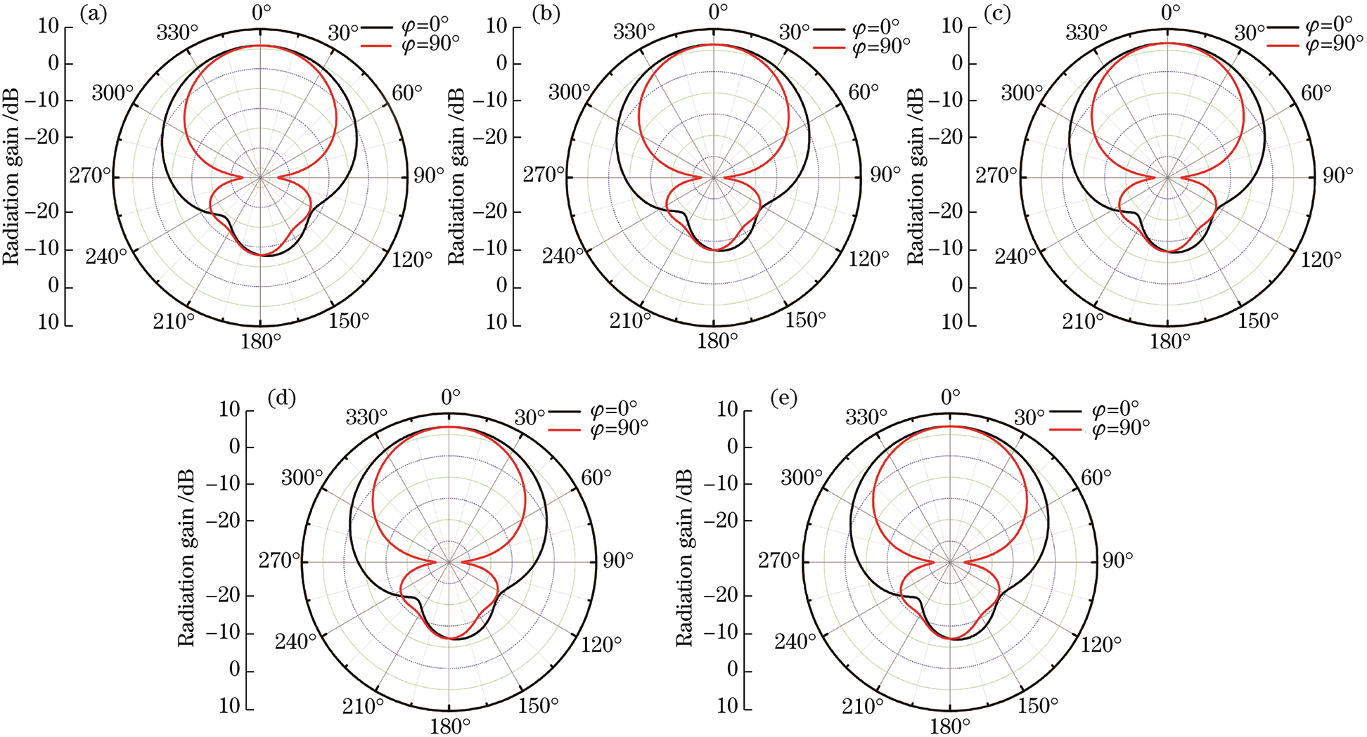
Figure 8: Comparison of the radiation pattern of the proposed antenna
As shown in Figs. 7 and 8, by controlling the chemical potential, the graphene-based frequency reconfigurable antenna can achieve 5 continuous working frequency bands, and has smaller backlobe radiation and better frontlobe radiation in the working frequency band. The specific antenna radiation performance is shown in Tab. 2.

It can be seen from Tab. 2 that when the chemical potential increases, the antenna radiation efficiency increases and the relative impedance bandwidth decreases. The influence of the chemical potential on the antenna operating frequency is consistent with the research results based on the equivalent circuit model. Based on the designed antenna structure (Figs. 6a and 6b) and expressions (5)∼(7), a numerical model is established to obtain the input impedance curve, which reveals the antenna resonance characteristics and the graphene variable surface conductance rate relationship. According to the reference [38], the value of the circuit component parameters such as radiation conductance and inductive capacitance can be calculated. The parameters of the equivalent circuit component are shown in Tab. 3.

From Eqs. (5)–(7), it can be seen that the surface conductivity σs of graphene is one of the antenna input admittance Yin, and the resonance characteristics of the graphene antenna can be obtained by changing the chemical potential, as shown in Fig. 9. It reveals the relationship between the chemical potential μc and the resonance frequency fres. The larger the chemical potential μc, the greater the resonance frequency fres. However, as the chemical potential μc increases, the control ability of graphene is limited, and the bias voltage is considered comprehensively. The influence of substrate dielectric constant and thickness on the chemical potential of graphene, the range of μc is 0~1 eV. When the designed antenna structure increases from 0 eV to 1 eV, the corresponding resonant frequency rises from 695.55 GHz to 705.05 GHz. When the specified antenna working frequency is between 695.55~705.05 GHz, it can pass Fine-tune the chemical potential (bias voltage) to realize the function of the antenna working at the specified frequency point; if the specified antenna working frequency is not within this range, you need to change the antenna structure or adjust the antenna size to realize the function of the antenna working at the specified frequency point. Based on the theoretical calculation and Ansys-HFSS simulation methods, the two curves obtained have the same trend, but there are differences. This is because the coupling effect between the microstrip transmission lines is ignored in the theoretical calculation.

Figure 9: Comparison of the fres of the proposed antenna
The antenna radiation characteristics in different references are shown in Tab. 4. The graphene frequency reconfigurable antenna has obvious advantages in radiation characteristics: when the resonant frequency is 705.05 GHz, the maximum radiation gain is 6.92 dBi (Tab. 2). Compared with the antenna in the references [31,43–46], the designed antenna radiation efficiency is higher.

The graphene-based frequency reconfigurable antenna has no external electronic components, and can work at 695.55, 698.10, 701.55, 703.15, 705.05 GHz and 5 resonance frequency points, and has 678.25~721.75 GHz. The graphene conductivity is changed by an external bias voltage to achieve antenna frequency tunability. An equivalent circuit model based on a graphene antenna is proposed, which explains the reason for the frequency tunability, and compares it with the simulation results of Ansys-HFSS The numerical calculation method further verifies the feasibility of the antenna design and helps to analyze the resonance performance of the antenna. Through simulation, the relative impedance bandwidth of each operating frequency band is greater than 4.5%. When the resonance frequency is 705.05 GHz, the radiation maximum gain is 6.92 dBi. When the resonance frequency is 695.55 GHz, the minimum radiation gain is 5.82 dB. Compared with other graphene-based terahertz antennas, the proposed antenna has a larger radiation gain. In addition, the radiation efficiency of the proposed antenna is much greater than that of traditional antennas. Therefore, the proposed graphene-based frequency reconfigurable antenna has advantages in terms of structure, radiation gain, and radiation efficiency.
Acknowledgement: The authors would like to thank the editors and reviewers for their review and recommendations.
Funding Statement: The authors received no specific funding for this study.
Conflicts of Interest: The authors declare that they have no conflicts of interest to report regarding the present study.
1. S. Y. Zhu, Y. L. Li, K. M. Luk and S. W. Pang, “Compact high-gain si-imprinted THz antenna for ultrahigh speed wireless communications,” IEEE Transactions on Antennas and Propagation, vol. 68, no. 8, pp. 5945–5954, 2020. [Google Scholar]
2. O. A. Saraereh, “A novel broadband antenna design for 5G application,” Computers, Materials & Continua, vol. 67, no. 1, pp. 1121–1136, 2021. [Google Scholar]
3. R. Xu, S. Gao, B. S. Izquierdo, C. Gu and P. Reynaert, “A review of broadband low-cost and high-gain low-terahertz antennas for wireless communications applications,” IEEE Access, vol. 8, pp. 57615–57629, 2020. [Google Scholar]
4. S. L. Mohammed, M. H. Alsharif, S. K. Gharghan, I. Khan and M. Albreem, “Robust hybrid beamforming scheme for millimeter-wave massive mimo 5G wireless networks,” Symmetry, vol. 11, no. 11, pp. 1–18, 2019. [Google Scholar]
5. S. Alemaishat, O. A. Saraereh, I. Khan, S. H. Affes, X. Li et al., “An efficient precoding scheme for millimeter-wave massive mimo systems,” Electronics, vol. 8, no. 9, pp. 1–15, 2019. [Google Scholar]
6. O. A. Saraereh, I. Khan, B. M. Lee and A. Al-Bayati, “Modeling and analysis of wearable antennas,” Electronics, vol. 8, no. 1, pp. 1–12, 2018. [Google Scholar]
7. C. Wang, Y. Yao, J. Yu and X. Chen, “3d beam reconfigurable THz antenna with graphene-based high impedance surface,” Electronics, vol. 8, no. 11, pp. 1–21, 2019. [Google Scholar]
8. S. E. Hosseininejad, M. Neshat, R. Dana, M. Lemme, P. H. Bolivar et al., “Reconfigurable THz plasmonic antenna based on few-layer graphene with high radiation efficiency,” Nanomaterials, vol. 8, no. 8, pp. 1–18, 2018. [Google Scholar]
9. C. Lee and J. Jeong, “THz cmos on-chip antenna array using defected ground structure,” Electronics, vol. 9, no. 7, pp. 1–14, 2020. [Google Scholar]
10. F. Zhao, C. Zhu, W. Guo, J. Cong, C. Tee et al., “Resonant tunneling diode (RTD) terahertz active transmission line oscillator with graphene-plasma wave and two graphene antennas,” Electronics, vol. 8, no. 10, pp. 1–16, 2019. [Google Scholar]
11. S. Fajr, A. Rajawat and S. H. Gupta, “Design and optimization of THz antenna for onbody wban applications,” Optik, vol. 223, pp. 1–12, 2020. [Google Scholar]
12. S. Ullah, C. Ruan, T. Haq and X. Zhang, “High performance THz patch antenna using photonic band gap and defected ground structure,” Journal of Electromagnetic Waves and Applications, vol. 33, no. 15, pp. 1943–1954, 2019. [Google Scholar]
13. A. K. Geim and K. S. Novoselov, “The rise of graphene,” Nature Materials, vol. 6, no. 3, pp. 183–191, 2007. [Google Scholar]
14. J. Diaz and J. P. Carrier, “Microwave to THz properties of graphene and potential antenna applications,” in IEEE Int. Symposium on Antennas and Propagation (ISAPNagoya, Japan, pp. 239–242, 2012. [Google Scholar]
15. J. P. Carrier, M. Tamagone, J. G. Diaz and E. Carrasco, “Graphene antenna: can integration and recofigurability compensate for the loss?” in European Microwave Conf., Nuremberg, Germany, pp. 141–148, 2013. [Google Scholar]
16. X. Zhang, C. Ruan and J. Dai, “Reconfigurable antenna based on graphene at terahertz frequency,” in Progress in Electromagnetic Research Symposium (PIERSToyama, Japan, pp. 1–7, 2018. [Google Scholar]
17. N. Hussain and I. Park, “Design of a wide-gain-bandwidth metasurface antenna at terahertz frequency,” AIP Advances, vol. 25, no. 5, pp. 1–12, 2017. [Google Scholar]
18. N. Hussain, T. K. Ngyuyen, H. Han and I. Park, “Minimum lens size supporting the leaky-wave nature of slit dipole antenna at terahertz frequency,” International Journal of Antennas and Propagation, vol. 5826957, pp. 1–8, 2016. [Google Scholar]
19. N. Hussain and I. Park, “Performance of multiple-feed metasurface antennas with different numbers of patch cells and different substrate thicknesses,” Applied Computational Electromagnetics Society Journal, vol. 33, no. 1, pp. 49–55, 2018. [Google Scholar]
20. Q. Rubani, S. H. Gupta, S. Pani and A. Kumar, “Design and analysis of a terahertz antenna for wireless body area networks,” Optik, vol. 179, pp. 684–690, 2019. [Google Scholar]
21. M. E. Temmar, A. Hocini, D. Khedrouche and M. Zamani, “Analysis and design of a terahertz microstrip antenna based on a synthesized photonic bandgap substrate using BPSO,” Journal of Computational Electronics, vol. 18, pp. 231–240, 2019. [Google Scholar]
22. F. Zhao, L. Mao, W. Guo, S. Xie and C. A. Tee, “On-chip terahertz detector designed with inset-feed rectangular patch antenna and catadioptric lens,” Electronics, vol. 9, no. 6, pp. 1–14, 2020. [Google Scholar]
23. K. S. Novoselov, A. K. Geim, S. V. Morozov, D. Jiang, Y. Zhang et al., “Electric field effect in atomically thin carbon films,” Science, vol. 306, no. 5696, pp. 666–669, 2004. [Google Scholar]
24. S. A. Amanatiadis, T. D. Karamanos and N. V. Kantartzis, “Radiation efficiency enhancement of graphene THz antennas utilizing metamaterial substrates,” IEEE Antennas and Wireless Propagation Letters, vol. 16, no. 5, pp. 2054–2057, 2018. [Google Scholar]
25. M. Donelli, “A simple and efficient adaptive ISM-band antenna based on a reconfigurable optically driven parasitic structure,” Electronics, vol. 7, no. 2, pp. 1–13, 2018. [Google Scholar]
26. K. Payandehjoo and R. Abhari, “Investigation of parasitic elements for coupling reduction in multiantenna hand-set devices,” International Journal of RF and Microwave Computer-Aided Engineering, vol. 24, no. 1, pp. 1–10, 2014. [Google Scholar]
27. Z. Li, Z. Du, M. Takahashi and K. Saito, “Reducing mutual coupling of MIMO antennas with parasitic elements for mobile terminals,” IEEE Transactions on Antennas and Propagation, vol. 60, no. 2, pp. 473–481, 2012. [Google Scholar]
28. I. Nadeem and D. Y. Choi, “Study on mutual coupling reduction technique for MIMO antennas,” IEEE Access, vol. 7, pp. 563–586, 2018. [Google Scholar]
29. S. Y. Zhu, Y. L. Li, K. M. Luk and S. W. Pang, “Compact high-gain si-imprinted THz antenna for ultrahigh speed wireless communications,” IEEE Transactions on Antennas and Propagation, vol. 68, no. 8, pp. 5945–5954, 2020. [Google Scholar]
30. M. S. Rabbani and H. G. Shiraz, “Fabrication tolerance and gain improvements of microstrip patch antenna at terahertz frequencies,” Microwave and Optical Technology Letters, vol. 58, no. 8, pp. 1819–1824, 2016. [Google Scholar]
31. S. Anand, D. S. Kumar, R. J. Wu and M. Chavali, “Graphene nanoribbon based terahertz antenna on polyimide substrate,” Optk, vol. 125, no. 19, pp. 5546–5549, 2014. [Google Scholar]
32. V. P. Gusynin, S. G. Sharapov and J. P. Carbotte, “Magneto-optical conductivity in graphene,” Journal of Physics, vol. 19, no. 2, pp. 231–241, 2007. [Google Scholar]
33. L. A. Falkovsky and S. S. Pershoguba, “Optical far-infrared properties of a graphene monolayer and multilayer,” Physical Review B, vol. 76, no. 15, pp. 1–17, 2007. [Google Scholar]
34. Y. M. Lin, K. A. Jenkins, A. V. Garcia, J. P. Small, D. B. Farmer et al., “Operation of graphene transistors at gigahertz frequencies,” Nano Letters, vol. 9, no. 1, pp. 422–426, 2009. [Google Scholar]
35. G. W. Hanson, “Dyadic green's functions for an anisotropic, non-local model of biased graphene,” IEEE Transactions on Antennas and Propagation, vol. 56, no. 3, pp. 747–757, 2008. [Google Scholar]
36. L. A. Falkovsky and S. S. Pershoguba, “Optical far-infrared properties of a graphene monolayer and multilayer,” Physical Review B, vol. 76, no. 15, pp. 1–19, 2007. [Google Scholar]
37. V. Ryzhii, A. Satou and T. Otsuji, “Plasma waves in two-dimensional electron-hole system in gated graphene heterostructures,” Journal of Applied Physics, vol. 101, no. 2, pp. 667–673, 2007. [Google Scholar]
38. L. A. Falkovsky, “Unusual field and temperature dependence of the hall effect in graphene,” Physical Review B, vol. 75, no. 3, pp. 1073–1085, 2007. [Google Scholar]
39. W. Richards, Y. Lo and D. Horrison, “An improved theory for microstrip antennas and applications,” IEEE Transactions on Antennas and Propagation, vol. 29, no. 1, pp. 38–46, 1981. [Google Scholar]
40. R. Kaul, “Microwave engineering,” IEEE Potentials, vol. 8, no. 2, pp. 11–13, 1989. [Google Scholar]
41. Z. K. Liu, Y. N. Xie, L. Geng, K. Pan and S. Pan, “Scattering of circularly polarized terahertz waves on a graphene nanoantenna,” Chinese Physics Letters, vol. 33, no. 2, pp. 3341–3352, 2016. [Google Scholar]
42. K. R. Jha and G. Singh, “Effect of low dielectric permittivity on microstrip antenna at terahertz frequency,” Optik, vol. 124, no. 22, pp. 5777–5780, 2013. [Google Scholar]
43. A. S. Thampy, M. S. Darak and S. K. Dhamodharan, “Analysis of graphene based optically transparent patch antenna for terahertz communications,” Physica E, vol. 66, pp. 67–73, 2015. [Google Scholar]
44. J. Li, M. He, C. B. Wu and C. Zhang, “Radiation pattern reconfigurable graphene leaky-wave antenna at terahertz band based on dielectric grating structure,” IEEE Antenna and Wireless Propagation Letters, vol. 16, pp. 1771–1775, 2017. [Google Scholar]
45. A. Sharma, V. K. Dwivedi and G. Singh, “THz rectangular patch microstrip antenna design using photonic crystal as substrate,” in Progress in Electromagnetic Research Symposium, USA, pp. 161–165, 2008. [Google Scholar]
46. N. Z. Rashed and H. A. Sharshar, “Optical microstrip patch antennas design and analysis,” Optik, vol. 124, no. 20, pp. 4331–4335, 2013. [Google Scholar]
 | This work is licensed under a Creative Commons Attribution 4.0 International License, which permits unrestricted use, distribution, and reproduction in any medium, provided the original work is properly cited. |