DOI:10.32604/iasc.2022.021558
| Intelligent Automation & Soft Computing DOI:10.32604/iasc.2022.021558 | |
| Article |
Performance Analysis of Low Power Interference Cancellation Architecture for OFDM System
1Department of Electronics and Communication Engineering, Malla Reddy Engineering College, Secunderabad, 500100, India
2Department of Electronics and Communication Engineering, Dayanandasagar College of Engineering, Bangalore, 560078, India
3Department of Electronics and Communication Engineering, Erode Sengunthar Engineering College, Erode, 638057, India
4Department of Wireless Communication, Institute of Electronics and Communication Engineering, Saveetha School of Engineering, Saveetha Institute of Medical and Technical Sciences, Chennai, India
*Corresponding Author: N. Manikanda Devarajan. Email: nmdevats@gmail.com
Received: 06 July 2021; Accepted: 07 August 2021
Abstract: Orthogonal Frequency Division Multiplexing (OFDM) is a wireless communication technology that is used for highly reliable and high data rate communication. In a multi-user OFDM system, the interference has occurred in the receiver side between the consecutive OFDM symbols. This interference reduces the performance of the OFDM system. To achieve good quality in received symbols the interference level should be minimized. The conventional cancellation system requires higher interference reduction time and power. These limitations of the conventional interference cancellation architectures for OFDM systems are overcome by proposing efficient and low power interference cancellation architecture. Hence, this paper proposes a novel and efficient architecture based on logic gates for interference cancellation in multi-user OFDM systems. The proposed design consist of multiplexers, inverters and OR gate. The heuristic parameters for the proposed cancellation architecture are computed by performing an XOR operation. Compared to existing architecture, the proposed interference cancellation architecture consumes 7 mW of power consumption in the Virtex processor, 33.59 mW of power consumption in Spartan 3E processor and 0.029 mW of power consumption in the CPLD processor. This proposed interference cancellation architecture consumes fewer hardware resources and consumes low power. The proposed system is designed using Verilog High Definition Language (HDL) and synthesized in Xilinx Project Navigator 12.1i. Further, this paper also proposes gate diffusion input (GDI) based implementation of proposed interference cancellation architecture to analyse a delay and power consumption compared to other logic style implementation.
Keywords: Wireless communication; low power; interference; hardware resources; data rate
The design of low power VLSI systems is an emerging trend in all fields like sensor networks, image processing and communication systems [1]. Modern communication methodologies require high-speed data transmission and a low error rate on the received signals. Orthogonal Frequency Division Multiplexing (OFDM) is a recent wireless communication technique that is an advanced version of the Code Division Multiple Access (CDMA) technique. In OFDM, the input signals are split into a number of sub-signals and each sub-signal is individually transmitted over the time-varying communication wireless channel. At present, the OFDM system exhibits the bandwidth overlap problem [2] which leads to the formation of interference in OFDM symbols. This paper provides the solution methodology for this present problem of the OFDM system.
The multi carrier modulation technique is used for the transmission and reception of signals in the OFDM system, in which the space between carrier symbols is unique and linear. The orthogonality property is applied between two adjacent signals. The existing OFDM systems have their dot product is zero. For verifying the orthogonality property in OFDM symbols, the two adjacent symbols in the OFDM system are convolved with each other. These two signals are said to be orthogonal to each other if the convolution response is zero. The non-zero response value will be produced if their convolved products are not orthogonal with each other. In the case of orthogonality checking, proper carrier spacing will be applied between adjacent symbols in OFDM system. During overlapping of carrier spacing between adjacent symbols in OFDM system, interference will have occurred between received symbols in OFDM system. The interference due to overlapping of carrier signals in OFDM system is called Inter-Carrier Interference (ICI). This ICI will degrade the quality of the OFDM system in both cases of symbol transmission and reception.
Fig. 1 shows the overview of the interference cancellation system in OFDM. It consists of an Interference estimator and Interference cancellation architecture. The interference estimator estimates the interference ratio between adjacent symbols in a receiver of the OFDM system. These interference reduced symbols are given to the multi-user OFDM system. This paper is organized as Section 2 discusses the various conventional architectures for interference cancellation architectures for OFDM systems in wireless less communication and Section 3 proposes a novel and efficient low power interference cancellation architecture is proposed. Section 4 discusses the experimental results and finally, Section 5 concludes this paper.

Figure 1: Overview of interference cancellation system in OFDM
Quan et al. [3] have proposed an Interference cancellation circuit for FFT based OFDM system and Discrete Cosine Transform based OFDM system. It estimated the level of interference in both types of OFDM systems. The authors achieved 48 dB for FFT based OFDM system and 52.5 dB for DCT based OFDM system. The authors also mapped one data symbol on three subcarriers which improve carrier to interference ratio (CIR) and BER, while the bandwidth efficiency was reduced by one third. The authors used the interference cancellation technique and dirty coding algorithms on the received subcarriers. Chanderkanta et al. [4] analyzed co-channel interference in received OFDM symbols. The authors estimated and analyzed the co-channel interference in terms of bit error rate and peak power ratio parameters. The authors analyzed the iterative cancellation methods on the OFDM system and compared the complexity of the proposed architectures with conventional architectures.
Pareyani et al. [5] developed low power architecture for the cancellation of intersymbol interference in received OFDM symbols. The four numbers of subcarrier frequency signals were used to modulate the single data OFDM symbol in the transmission section of the OFDM system. This affected the linear interference cancellation in the reception side of the OFDM system. The authors used an Additive White Gaussian Noise channel environment for the simulation of their proposed OFDM system. The authors achieved a low bit error rate even the system was designed in a highly noisy environment. Fan et al. [6] used the least square algorithm for the transmission channel of the OFDM system. This algorithm was used by the authors to detect and cancel the interference between the OFDM symbols. Lee et al. [7] devised a polynomial fitting technique to estimate the condition of the channel in order to reduce the effect of interference between received OFDM symbols in the OFDM system. Zhao et al. [8] introduced an ICI self-cancellation technique. In this technique, one data symbol was mapped on two subcarriers at the transmitter side and at the receiver side these groups of subcarriers are combined so the effects of ICI on these subcarriers cancelled each other. This scheme was easy to implement but the bandwidth efficiency was reduced. . Gowshameed et al. [9] developed the interference detection technique for the reduction of interference in the received OFDM symbols.
Zhou et al. [10] and Devarajan et al. [11] have proposed a balanced detection based noise cancellation technique in FDMA.it can also be used in the optical line. The proposed architecture achieves low power with a minimum bit error rate.it also reduces the signal-to-signal beat interference effectively. Adegbite et al. [12] and Myllyla et al. [13] have proposed a time-domain detection method for block-level detection. The proposed method only uses the correlation of data to detect an error in transmitted and received information. There is no additional hardware needed for detection. compared to Maximum Likelihood method, the proposed method shows better detection efficiency.
Hori et al. [14] and Boher et al. [15] have proposed a power-efficient detector design technique for millimeter-wave multi-input-multi-output (MIMO) transceivers. A novel method is proposed to allow multi-antenna frequency-division-duplex (FDD) and full-duplex (FD) operation. Compared to other designs, the proposed design attains low power operation for all bit sizes. Mohammed et al. [16] have proposed a noise compensation method for low power IoT applications. Dual-mode receiver designed for sending larger data size. The proposed architecture is implemented in an FPGA device to evaluate area and power. Results show that the proposed method achieves low power consumption compared to other design techniques.
The following points are observed from the conventional interference cancellation architectures for the OFDM system.
• The conventional architectures consumed high power consumption due to their complex design.
• Higher interference reduction time.
These limitations of the conventional interference cancellation architectures for OFDM systems are overcome by proposing efficient and low power interference cancellation architecture.
The popularity of the OFDM modulation system in communication motivates the researchers to design a low power consuming OFDM. The hardware parts of memory, encoder and decoders are optimized to reduce get overall power reductions. This work concentrates on the low power noise cancellation technique for the OFDM system. In a multi-user OFDM system, there is interference between transmitted OFDM symbols which degrades the signal quality at the receiver end. In this paper, an efficient low power Interference estimator and cancellation architecture is proposed in the receiver end of the OFDM system in order to increase the quality level of the received symbols. Fig. 2 shows the Interference estimator architecture which estimates the presence of interference in the received OFDM symbols. The following circuit generates four-bit sequenced output patterns as dataout1 and dataout2 for the four-bit sequenced input patterns as data1 and data2. The bit error rate is a parameter to compute the variations of the output pattern with respect to the input pattern. It is defined as the ratio between the numbers of variance bits for dataout1 to the total number of bits in the input pattern. If the bit error rate of dataout1 and dataout2 shows more than 50% variance with respect to input patterns, it shows the presence of the interference in the received OFDM symbols.

Figure 2: Interference estimator
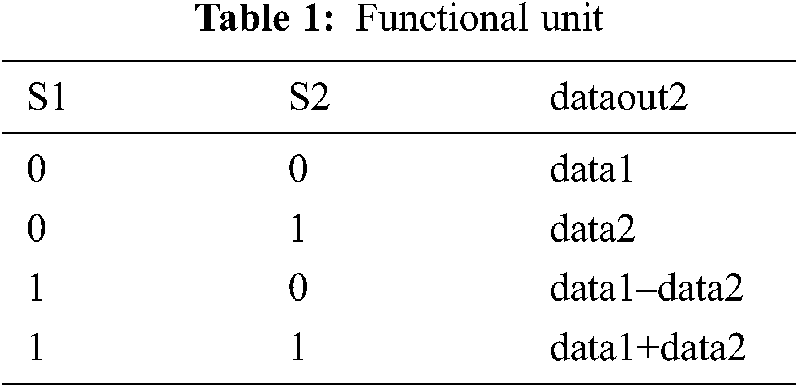
Tab. 1 shows the logic table of the functional unit used in Interference estimator circuit. If the control signals s1 = 0 & s2 = 0, then data1 is assigned to dataout2. If the control signals s1 = 0 & s2 = 1, then data2 is assigned to dataout2. If the control signals s1 = 1 & s2 = 0, then data1-data2 is assigned to dataout2. If the control signals s1 = 1 & s2 = 1, then data1+data2 is assigned to dataout2.
If the level of interference is more than the threshold value, then there is a need for interference cancellation architecture. In this paper, a novel and efficient Interference cancellation architecture for OFDM system in low power applications. For the case of multi user OFDM system, the interference level is high between adjacent symbols. This interference level should be minimized in order to improve the quality of the received symbols. Fig. 3 shows the low power interference cancellation architecture which can be designed using gates logic and multiplexers. The proposed interference cancellation architecture is incorporated in a receiver of the multi-user OFDM system. It receives datain1 and datain2 as four bits input patterns. The data retention is achieved in the receiver side of multi-user OFDM system due to the implementation of interference cancellation architecture with XOR gates. Based on the number of bit patterns in datain1 and datain2, the heuristic parameters are computed. The heuristic parameters for the proposed interference cancellation architecture are given as,

Figure 3: Interference cancellation architecture
The select lines c0 and c1 for the multiplexers are chosen based on the number of one's in the received sequences. The select lines c0 = 1 and c1 = 1 are set if the numbers of ones in datain1 are greater than the numbers of ones in datain2, otherwise, the values of these select lines are set to c0 = 0 and c1 = 0. The concatenation and sorter block performs two kinds of operations as grouping the output patterns and sorting the output bit patterns in a linear order. This concatenation and sorter block produces two 4-bits output patterns as shown in Fig. 3.
The level converter for the proposed interference cancellation architecture is shown in Fig. 4. This proposed converter circuit is based on the multiplexers, inverters and OR gate. It has two inputs and single output as shown in Fig. 4.

Figure 4: Level converter
GDI Implementation of Proposed Cancellation Architecture
In VLSI design methodology, various logic styles are available to design logic circuits like Complementary Pass Transistor Logic (CPL), transmission gate based logic, pass transistor logic and Dual Pass Transistor Logic (DPL) etc. Recently, compared to other styles GDI based logic design attracted by designers by its simple structure and low power implementation. The structure of the GDI cell is shown in Fig. 5. It has three terminals. Both N-MOS and P-MOS gates are connected to form a common gate. The remaining two terminals are denoted as P and N.

Figure 5: GDI basic cell
Above Tab. 2. Explain the functionality of the GDI cell. We can implement all other logic functions using GDI cells with minimum transistor requirements. In this paper, the cancellation architecture components of XOR gates, Mux's and sorter units are designed using GDI logic. Fig. 6 shows the GDI design of the XOR gate. Besides, the layout of the proposed GDI architecture is shown in Fig. 7.
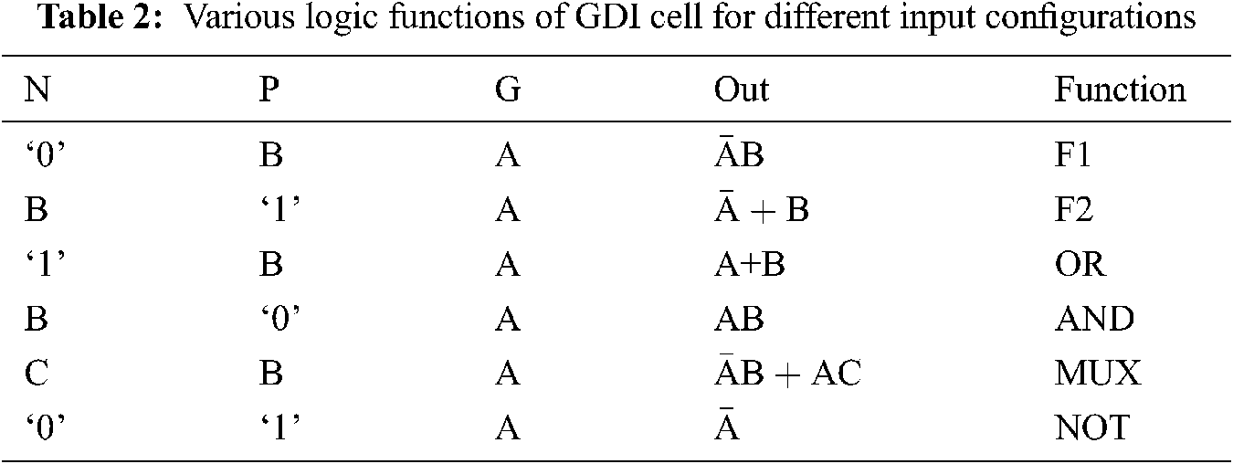

Figure 6: GDI-XOR gate

Figure 7: Layout of proposed GDI architecture
In this paper, Modelsim 6.1i simulating tool and Xilinx project navigator 12i synthesis tool are used to conduct the experiment for OFDM system interference reduction. The proposed system is coded in Verilog language. Fig. 8a shows the signal flow graph of the proposed interference cancellation architecture using Modelsim software and Fig. 8b shows the waveform results of the proposed system.

Figure 8: Simulation results of the proposed system (a) Signal flow graph (b) Waveform
Fig. 9a shows the schematic diagram of the proposed interference cancellation architecture using Xilinx project navigator tool. Figs. 9b and 9c illustrate the RTL and technology schematic view of the proposed interference cancellation architecture. The internal perspective of the proposed design or architecture can be view in the RTL diagram, whereas the layered perspective of the proposed design can be view in the technology diagram.

Figure 9: (a) Schematic diagram (b) RTL schematic view (c) Technology schematic view
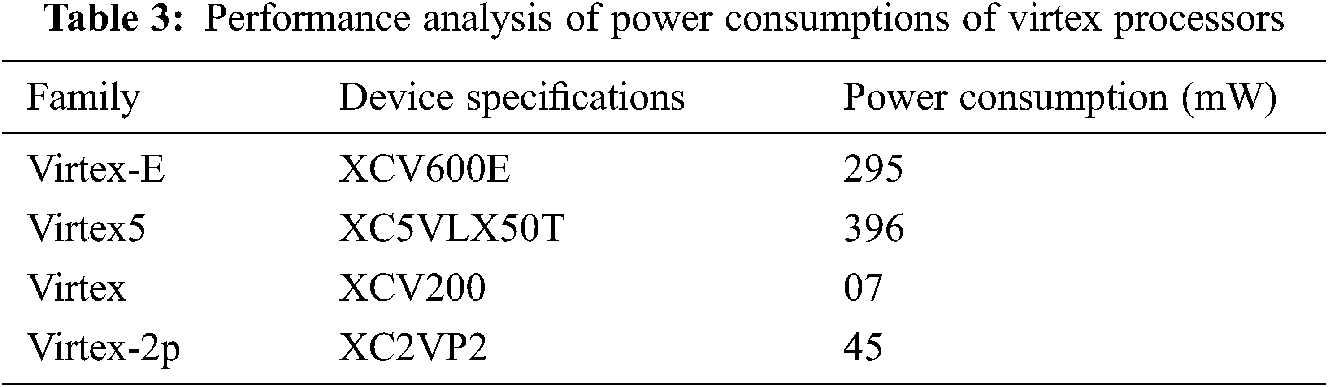
The proposed architecture is tested on different Virtex processors with different specifications. Virtex family with XCV200 processor consumes 7 mW of power consumption, which is low power consumption than the other devices in Virtex family. This is illustrated in Tab. 3.
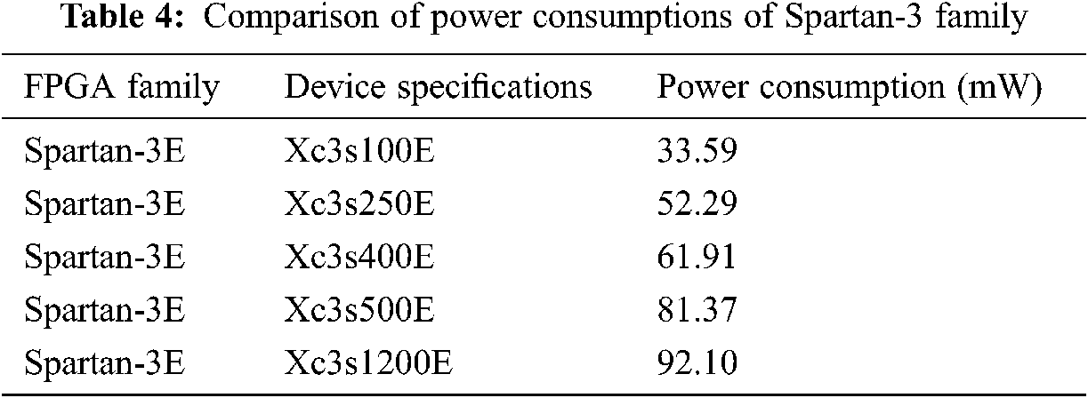
The proposed architecture is tested on different Spartan−3E processors with different specifications. Spartan−3E family with Xc3s100E processor consumes 33.59 mW of power consumption, which is low power consumption than the other devices in Spartan 3E family. This is illustrated in Tab. 4.
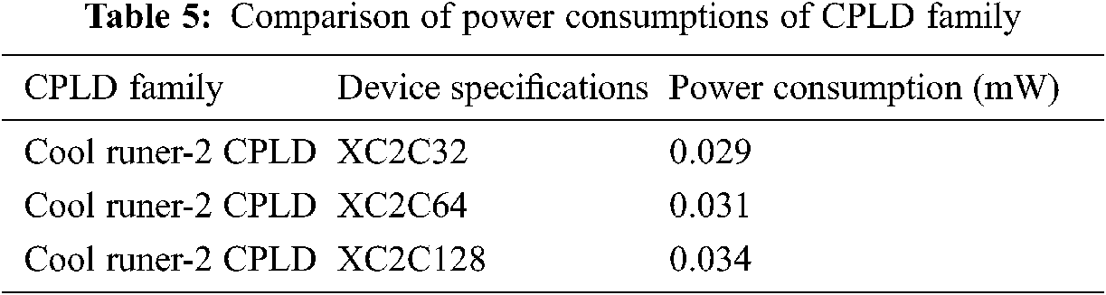
The proposed architecture is tested on different CPLD processors with different specifications. CPLD family with XC2C32 processor consumes 0.029 mW of power consumption, CPLD family with XC2C64 processor consumes 0.031 mW of power consumption and CPLD family with XC2C128 processor consumes 0.034 mW of power consumption. This is illustrated in Tab. 5.
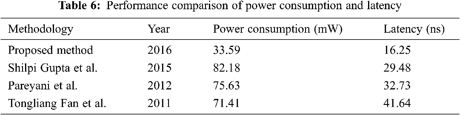
The power consumption of the proposed interference cancellation architecture is compared with the conventional techniques in Tab. 6. The conventional techniques as Shilpi Gupta et al. consumed 82.18 mW of power consumption, Pareyani et al. consumed 75.63 mW of power consumption and Tongliang Fan et al. consumed 71.41 mW of power consumption.
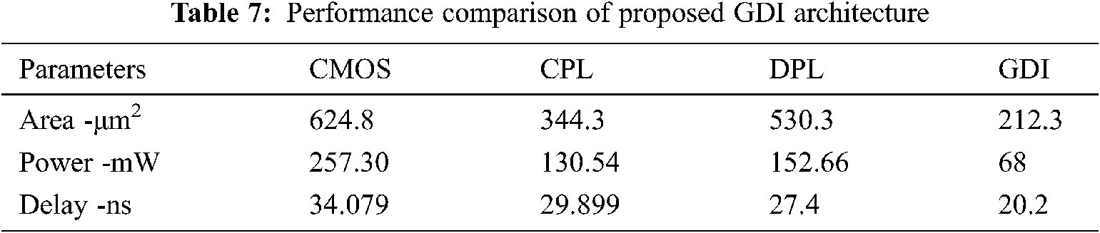
The performance of GDI implementation of the proposed cancellation architecture is tabulated in Tab. 7. From the results observed that proposed architecture achieves higher area and delay reduction compared to other logic styles like CMOS, Complementary Pass Transistor Logic (CPL) and Dual Pass Transistor Logic (DPL) etc. The overall power consumption also reduces considerably.
In this paper, low power architecture for interference cancellation for multi-user OFDM systems is proposed. The proposed system is simulated using Modelsim software and synthesized using Xilinx Project Navigator. RTL and Technology schematic of the proposed interference cancellation architecture are analyzed. The proposed interference cancellation architecture consumes 7 mW of power consumption in the Virtex processor, 33.59 mW of power consumption in the Spartan 3E processor and 0.029 mW of power consumption in the CPLD processor. The overall 22% power reduction was achieved by the proposed architecture. The latency rate of the proposed interference cancellation architecture in multi-user OFDM is about 16.25 ns. In addition, the proposed GDI based cancellation architecture outperforms in terms of energy, delay and power consumption.
Funding Statement: The authors received no specific funding for this study.
Conflicts of Interest: The authors declare that they have no conflicts of interest to report regarding the present study.
1. B. Sakthivel and A. Padma, “Area and delay efficient GDI based accuracy configurable adder design,” Microprocessors and Microsystems, vol. 73, no. 1, pp. 102958–102967, 2019. [Google Scholar]
2. A. S. Gupta, U. Dalal and V. N. Mishra, “Performance on ICI self-cancellation in FFT-OFDM and DCT-OFDM system,” Journal of Function Spaces, vol. 3, no. 5, pp. 1–7, 2015. [Google Scholar]
3. X. Quan, Y. Liu and S. Shao, “Impacts of phase noise on digital self-interference cancellation in full-duplex communications,” IEEE Transactions on Signal Processing, vol. 65, no. 7, pp. 1881–1893, 2017. [Google Scholar]
4. S. Chanderkanta and S. Singh, “Equalization of OFDM by iterative ICI reduction methods,” International Journal of Advanced Research in Computer and Communication Engineering, vol. 4, no. 3, pp. 1–6, 2015. [Google Scholar]
5. S. Pareyani and P. Patel, “An improved ICI self cancellation method to reduce ICI in OFDM systems,” International Journal of Innovative Technology and Exploring Engineering, vol. 1, no. 6, pp. 27–31, 2012. [Google Scholar]
6. T. Fan, H. Wu and H. Huang, “Channel estimation and interference cancellation for OFDM systems based on total least squares solution,” Journal of Communications, vol. 6, no. 8, pp. 640–647, 2011. [Google Scholar]
7. H. Lee, B. Lee and I. Lee, “Iterative detection and decoding with an improved V-BLAST for MIMO-OFDM systems,” IEEE Journal on Selected Areas in Communications, vol. 24, no. 3, pp. 504–513, 2006. [Google Scholar]
8. Y. Zhao and S. G. Haggman, “Intercarrier interference self-cancellation scheme for OFDM mobile communication systems,” IEEE Transactions on Communications, vol. 49, no. 7, pp. 1185–1191, 2001. [Google Scholar]
9. S. Gowshameed and R. Chanemougapriya, “IBI and ICI cancellation for MIMO OFDM based on tomlinson harashima precoder and dirty paper coding,” International Journal of Science, Engineering and Technology Research, vol. 4, no. 2, pp. 325–329, 2015. [Google Scholar]
10. A. Zhou and J. Ma, “A novel multi-band OFDMA-PON architecture using signal-to-signal beat interference cancellation receivers based on balanced detection,” Photonic Network Communications, vol. 32, no. 1, pp. 54–60, 2015. [Google Scholar]
11. N. M. Devarajan and M. Chandrasekaran, “Design and FPGA implementation of reconfigurable OFDM with improved PAPR,” Optoelectronics and Advanced Materials–Rapid Communications, vol. 9, no. 5, pp. 561–566, 2015. [Google Scholar]
12. S. A. Adegbite, S. G. McMeekin and B. G. A. Stewart, “Selective control information detection scheme for OFDM receivers,” Telecommunication Systems, vol. 64, no. 1, pp. 31–41, 2016. [Google Scholar]
13. M. Myllyla, M. Juntti and J. R. Cavallaro, “Implementation aspects of list sphere decoder algorithms for MIMO-OFDM systems,” Signal Processing, vol. 90, no. 10, pp. 2863–2876, 2010. [Google Scholar]
14. Y. Hori and H. Ochiai, “A low PAPR subcarrier hopping multiple access with coded ofdm for low latency wireless networks,” In IEEE Global Communications Conference (GLOBECOMSan Diego, CA, USA, pp. 1–6, 2014. [Google Scholar]
15. L. Boher, R. Rabineau and M. Helard, “FPGA implementation of an iterative receiver for MIMO-OFDM systems,” IEEE Journal on Selected Areas in Communications, vol. 26, no. 6, pp. 857–866, 2008. [Google Scholar]
16. A. Z. Mohammed, A. K. Nain, J. Bandaru and A. Kumar, “A residual phase noise compensation method for IEEE 802.15.4 compliant dual-mode receiver for diverse low power IoT applications,” IEEE Internet of Things Journal, vol. 1, no. 1, pp. 23–32, 2018. [Google Scholar]
 | This work is licensed under a Creative Commons Attribution 4.0 International License, which permits unrestricted use, distribution, and reproduction in any medium, provided the original work is properly cited. |