DOI:10.32604/iasc.2022.021663
| Intelligent Automation & Soft Computing DOI:10.32604/iasc.2022.021663 | |
| Article |
Energy Conservation of Adiabatic ECRL-Based Kogge-Stone Adder Circuits for FFT Applications
1Sri Ranganathar Institute of Engineering and Technology, Coimbatore, 641110, India
2SSM Institute of Engineering and Technology, Dindigul, 624002, India
*Corresponding Author: P. Dhilipkumar. Email: kumar.dhilip161@gmail.com
Received: 09 July 2021; Accepted: 01 September 2021
Abstract: Low Power circuits play a significant role in designing large-scale devices with high energy and power consumption. Adiabatic circuits are one such energy-saving circuits that utilize reversible power. Several methodologies used previously infer the use of CMOS circuits for reducing power dissipation in logic circuits. However, CMOS devices hardly manage in maintaining their performance when it comes to fast switching networks. Adiabatic technology is employed to overcome these difficulties, which can further scale down the dissipation of power by charging and discharging. An Efficient Charge Recovery Logic (ECRL) based adiabatic technology is used here to evaluate arithmetic operations in circuits like inverter, full adder, Carry Look-Ahead adder etc. A better chance at reducing delay in digital circuits is illustrated by developing a Kogge-stone Adder, built using the ECRL technology. The developed circuitry is further integrated into a Fast Fourier Transform (FFT), which demonstrates the circuit’s enhancement into DSP applications. Not only does this design reduce delay in VLSI switching circuits, but also narrows the power dissipation down to a minimum. This technique proved superior to the existing PFAL technique by demonstrating almost 10% less power dissipation with minimal propagation delay. All the circuits have been simulated at 45 nm technology using the Tanner EDA tool.
Keywords: Full adder; ECRL; carry look-ahead adder; kogge-stone; multiplexer; FFT
Designing techniques for low power consumption have vastly influenced the current electronic industry trend, due to the increasing demand for compact gadgets such as cellphones, laptops, and several other handheld devices. The microelectronics industry have immensely evolved since transistors were initially designed, which set forth the foundation for such devices. A large number of gadgets were designed by integrating several transistors in them. As the current portable devices necessitate a huge number of logic gates to assemble in a single integrated chip, the area (or) the size of the chip becomes a major concern. Presently, a single IC incorporates fabrication of around 100,000 or even more transistors in it, thusly calling it VLSI (very large scale integration) [1]. Due to the earlier VLSI technologies relying on speed optimization to improve its performance, it has often suffered from portability issues. Reducing the chip size leads to betterment in portability, but at the cost of more power consumption. Growing demands in less heat consumed, fast and portable gadgets have prompted several researchers to come up with several power reduction techniques. Some of them are discussed in this paper. There are different types into which power dissipation can be categorized [2]: 1) Static dissipation since there are leakage currents in the device, 2) Dynamic capacitive power owing to charge and discharge of device load capacitances, and 3) Short-circuit power dissipation, which happens because of the short circuit currents arising in CMOS. In [3–9], several adiabatic technologies have been reported. A combination of ECRL with a technique that diminishes gate leakage, simultaneously saving the correct logic state, known as the Sleepy Keeper approach, was implemented in [10,11]. The following figure (Fig. 1) depicts the flow of the proposed work starting from building the ECRL to the development of Kogge-stone adder circuit.
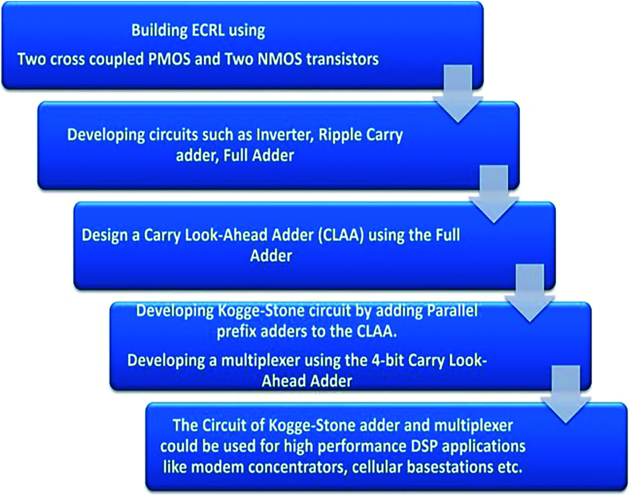
Figure 1: Scheme for the proposed work
This work makes use of the ECRL logic to build full adders and develop Kogge-Stone as well as multiplier circuits using the adder. Kogge-Stone is another VLSI architecture that employs minimum chip size and adiabatic method to improve power dissipation in devices. By cascading the architectures of multiplexer and Kogge-Stone circuits, the product can be pitched as a DSP application. The flow for the proposed work has been given in the following Fig. 1.
Basic implementations of several full-adder cells have been designed with modified logic styles, some of which have been compared with this work. Although they possess a similar functionality where intermediate nodes and outputs are created, the loads inside them have been changed. Several designs favour a single performance aspect at the cost of others. In some devices, full adders are created out of a single logical design whereas some designs possess multiple [12]. Complementary Pass-Transistor Logic (CPL) is used to produce outputs using several intermediate nodes and their complements. The CPL varies fundamentally with the complementary CMOS due to its pass logic electronics network design [13]. Scientific research in the current electronic industry has been challenged by its necessity to draw low energy, which suggests that the architectural and circuital solutions in electronic systems need to be investigated for reducing power dissipations. In order to reduce the dynamic power, an alternative approach was proposed in recent years, apart from the traditional techniques, named adiabatic switching [14,15]. Here, while the node capacitances undergo charging and discharging, minimal energy is wasted and recovered through the capacitors. Adiabatic circuits have been vastly studied in [16,17]. Several traditional CMOS adder circuits were compared in [18–22], and a comparison was also performed between the adiabatic families from [23–26]. This work focuses on examining adiabatic circuits against adder circuits like Kogge-Stone as well as a multiplexer, bringing it competitive with the conventional CMOS based circuits with respect to its transistor count and dissipated power. Eventually, a Finite Fourier Transform (FFT) is constructed with the KSA using Radix 4 format.
The remaining sections have been detailed as shown: Section 2 describes the related work regarding the description of ECRL Logic. Section 3 describes the proposed work of this paper. The outcomes explaining the power dissipation and the transistor count has been reported in Section 4. In Section 4, conclusions have been drawn.
The proposed work concentrates on designing Kogge-stone adder and multiplexer circuits and further enhance it into an FFT application, by using ECRL. This is performed by initially developing a full adder, ripple carry adder and Carry Look-Ahead Adder with this technology. This operation makes use of 4-bit functionality. The multiplexer minimizes the mux stages using the variable adder length feature and thus lowers the critical path. This in turn decreases the power dissipation of the circuit. This circuit will be developed into a device that can prove to be an efficient power-consuming candidate for DSP applications. ECRL is introduced in this paper by initially discussing adiabatic logic and its significance in adders.
Adiabatic, described from a thermodynamics process, illustrates that energy is not exchanged to the external environment, thereby stating that there will not be any chance of power or energy to dissipate. Adiabatic logic is beneficial in the switching process since power is not dissipated as heat energy through the resistor present there. It instead recycles back the power to the supply from the load capacitance, and the same energy (or) power is used for the next operation. The energy is recovered without any loss in the system and the heat is preserved. The energy is stored in load capacitors, in which the grounded charges will be recycled back to the power clock. Some of the various adiabatic techniques used in this paper have been explained below.
2.2 Efficient Charge Recharge Logic (Efficient Charge Recovery Logic) (ECRL)
Here, the pre-charge and evaluation phases are performed at the same time by eliminating the pre-charge diode and dissipating the energy at the same time, as compared to other adiabatic circuits. The proposed ECRL comprises two cross-coupled PMOS transistors and two NMOS transistors as N-functional blocks. The full swing output is obtained in both the pre-charge and recovery phase because of the two cross-coupled PMOS transistors. Fig. 2. shows the construction of Efficient Charge Recovery Logic (ECRL).
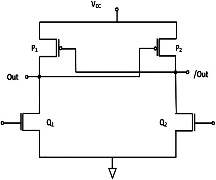
Figure 2: Basic ECRL circuit
The pre-charge and recover phases deliver complete output swings, owing to the presence of the cross-coupled PMOS transistors. However, when the threshold voltage of PMOS is attained by the supply clock voltage, the device turns off. Hence, the recovery path connecting to the clock comes about disconnected [27]. There is a sinusoidal clocked input voltage for the ECRL in our work, containing four phases for each cycle. They are: wait, evaluate, hold and recover. This fact is represented in Fig. 2. Due to an insignificant difference in voltage between the source and drain, there is a minor loss of energy in the logic, due to it being a quasi-adiabatic technique, where certain energy is returned back to the source. Owing to the impracticability to obtain full adiabatic operations, Quasi-adiabatic techniques have gained significance recently [28,29].
2.3 Implementation of Full Adder
The full adder logic takes in eight inputs, generating an adder that is a byte-wide, and adds a carry bit from one adder to the other. Full adder is implemented by making use of the ECRL, instead of the basic CMOS logic.
ECRL Based FA
A power clock initiates the logic to operate in four various phases: Wait, Evaluate, Hold and Recover.
i. Wait: the previous gate provides the input signal.
ii. Evaluate: stability of input signal is maintained.
iii. Hold: input kept at hold, meanwhile it is reduced, thereby keeping the supply voltage constant.
iv. Recover: “VDD” comes to zero position and becomes lower, and energy from the output node is recovered.
2.4 Carry Look-Ahead Adder Description
Recently, designers are considering important issues like high speed, small silicon area and low power consumption for developing digital circuits. The popular methodology among computational logic elements is binary addition. The carry look-ahead adder is also known as “Fast Adder”. Carry Look-Ahead Adder (CLAA )reduces the delay of the circuit not by generating an output that acts as another adder’s input, but by propagating to the combinational block.
The carry and sum outputs are
ECRL Implementation of Carry Look-Ahead Adder
Implementing this logic facilitates the transfer of some of the charges to the ground, thereby recovering part of the energy. The two PMOS transistors help to pull the power back to the AC supply. The summing circuit for the ECRL based CLAA circuit is shown in Fig. 3a. The construction of the circuit for carry in ECRL based CLAA is shown in Fig. 3b.
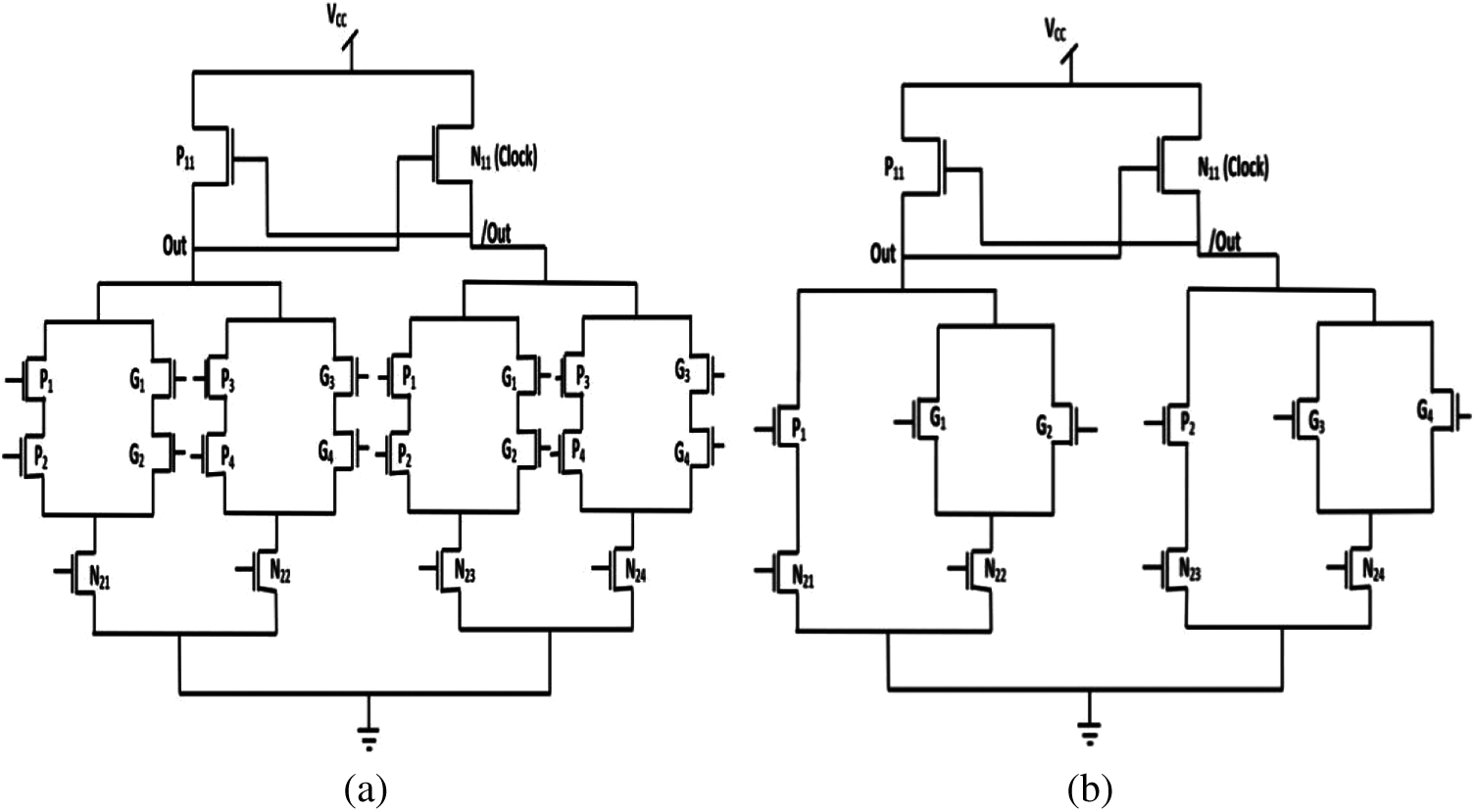
Figure 3: (a) Sum circuit of ECRL carry look-ahead adder, and (b) carry circuit of ECRL carry look-ahead adder
2.5 Kogge-Stone Adder Implementation
In addition to the performance of the CLAA, a Parallel Prefix Adder is developed for attaining better performance than other adders. It uses binary addition just like Carry look-ahead. Kogge-Stone adder is known as the fastest adder available, and a large number of recurrence problems are dealt with in this adder. Fig. shows the structure of Kogge-Stone adder circuit.
Fig. 4 shows the design of CLAA based 4-bit Kogge-Stone adder circuit implemented in this paper. It has architecture quite similar to that of CLAA. An added block would be the Fundamental Cary Operator (FCO) which handles the conversion of generator and propagator bits in the structure.
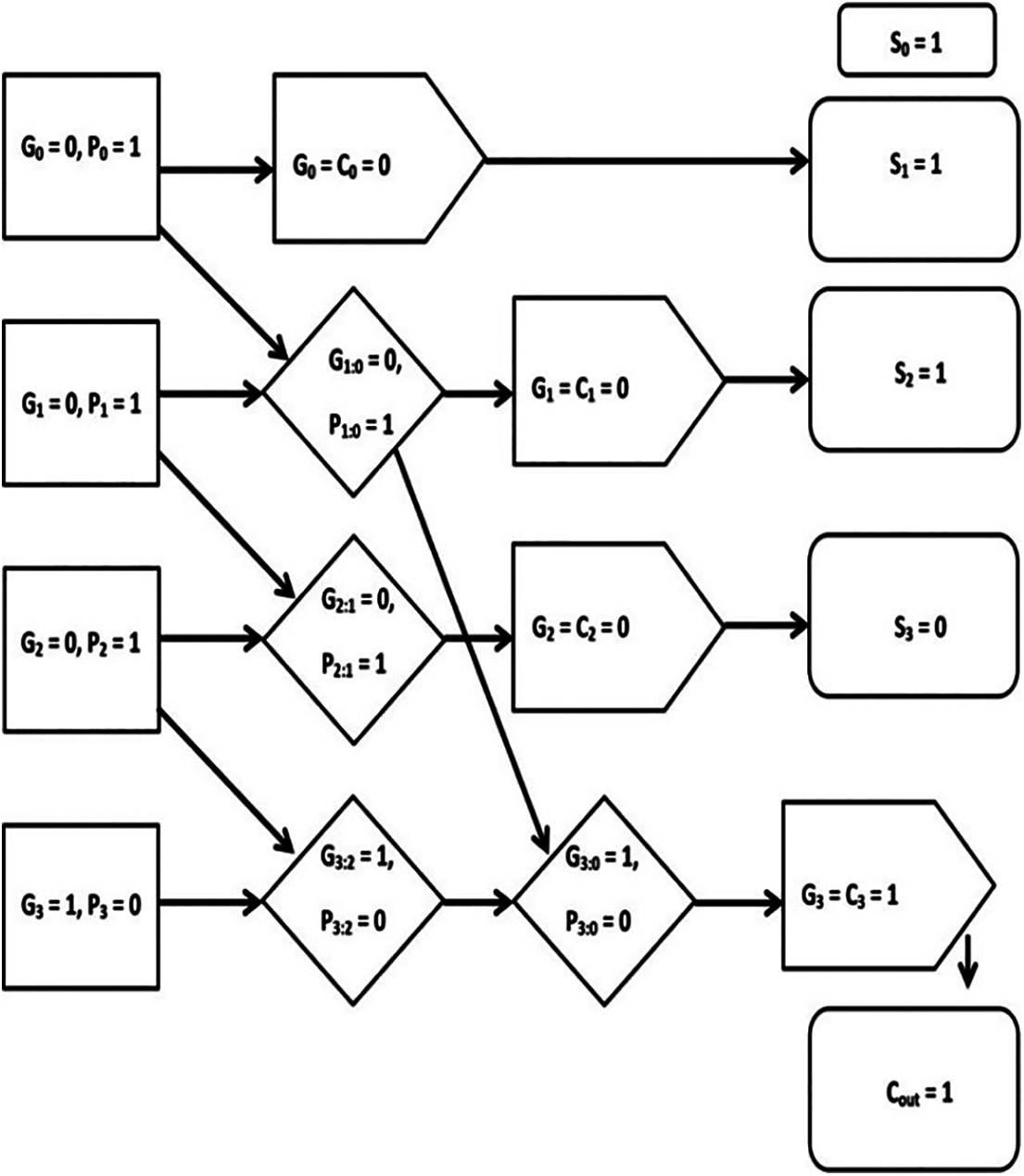
Figure 4: CLAA implementation of 4-bit kogge-stone adder
2.6 Multiplexer Implementation
A multiplexer circuit is implemented along with CLAA. Generally, CLAA and Ripple Carry Adder (RCA) will be used to operate the multiplexer function. Here since ECRL logic is used, only CLAA will be required for developing the circuit. In this following structure, the length of the adder will be variable for reducing the number of multiplexer stages which reduces the critical path, and eventually the power dissipation. Fig. 5 shows the implementation of mux stages along with CLAA.
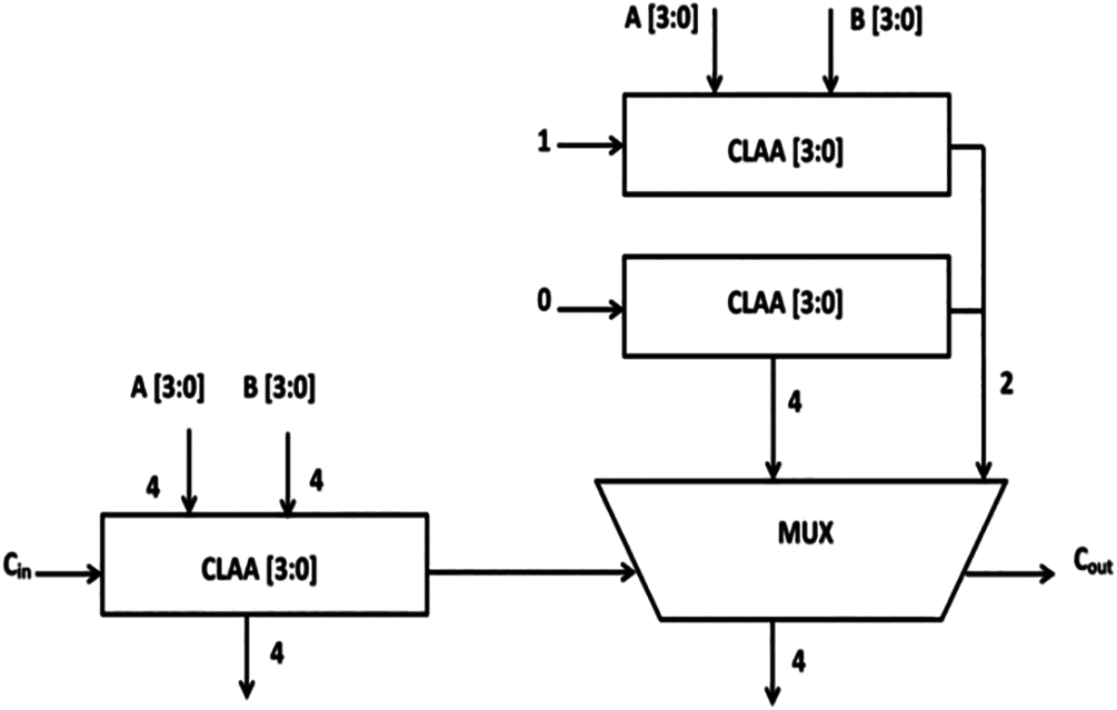
Figure 5: Implementation of multiplexer stages with the help of CLAA
Fig. 6 shows a radix 4 FFT architecture using a Single path Delay Feedback (SDF) structure. An SDF is required for developing an FFT structure using a complex circuit like Koggestone adder.
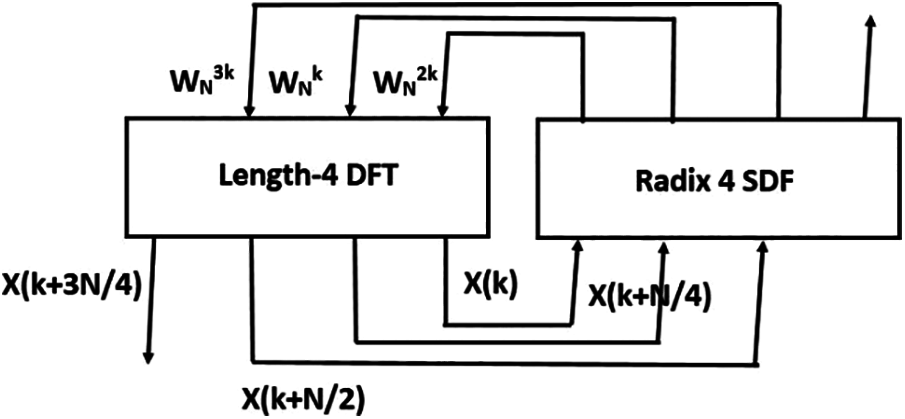
Figure 6: Implementation of radix 4 FFT using KSA
SDF utilizes the register more effectively by storing each output of the butterfly model inside the feedback shift registers. The Radix-4 butterfly comprises four inputs and outputs. The radix-4 FFT requires only 75% as many complex multiplies as the radix-2 FFTs, although it uses the same number of complex additions. These additional savings make it a widely-used FFT algorithm.
3 Results and Graphical Analysis
A representation of several circuits designed using the Tanner EDA tool is depicted in the following sections. A full adder, Ripple Carry Adder (RCA), Carry Look-Ahead Adder (CLAA) is developed using the proposed ECRL technique. The obtained results are compared with the conventional CMOS logic based respective circuits and attained much better and higher power dissipation values.
The outcomes of the proposed RCA circuit in ECRL technology had been simulated using 45 nm technology, in the Tanner EDA tool. Tanner EDA tool Software. When a = 0, b = 0, and c = 0, the obtained sum will be “0” and Cout is “0”. Whereas when a = 1, b = 1, and c = 1, the obtained sum will be “1” and Cout is “1”. Based upon the operation, the obtained Power Dissipation is 0.25 μW. A schematic representation in the Tanner EDA tool is shown in Fig. 7.
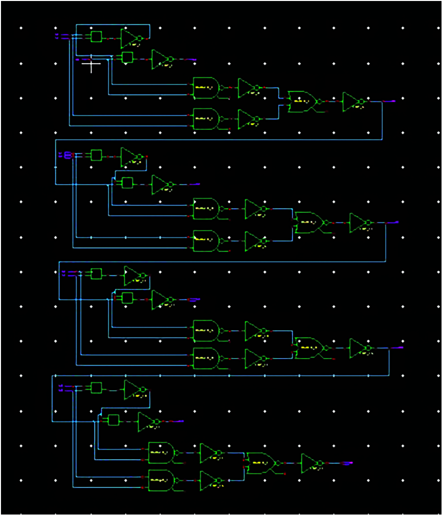
Figure 7: Schematic of ECRL based ripple carry adder
When a = 0, b = 0, and c = 1the obtained sum is “1” and Cout is “0”. When a = 0, b = 1, c = 1, the obtained sum is “0” and Cout is “1”. Whereas for the conventional CMOS logic, the obtained Power Dissipation is 0.79 μW.
3.2 Carry Look-Ahead Adder–Kogge-Stone Implementation
The ECRL-based Carry Look-Ahead Adder Circuit is also simulated by employing the 45 nm technology, in Tanner EDA tool. The Power Dissipation of CMOS Carry Look Ahead Adder is 6.0038 nW. The simulation result of ECRL-based Carry Look-Ahead Adder Circuit had been simulated by using 45 nm technology, mentor graphics EDA tool Software. The schematic of the CLAA based Kogge-Stone circuit is represented in Fig. 8.
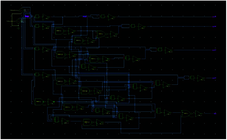
Figure 8: Schematic of ECRL based kogge-stone circuit using carry look-ahead adder
Fig. 7 shows the output waveforms for the proposed ECRL based CLAA when implemented in the Kogge-Stone circuit. The Power Dissipation amounts to 6000.38 nW. The main objective of this research is to reduce power and energy consumption. Which also means reducing the propagation delay. The inputs A and B in the above Kogge-Stone circuit tend to have initial values 0 and 0. The number of elements in the circuit will be directly proportional to the operation speed, or even the propagation delay. Since the transistor count in the ECRL is much lesser than the traditional CMOS logic, the proposed work has a lesser propagation delay.
The output waveform for the ECRL based Kogge-Stone circuit developed using Carry Look-Ahead Adder is shown in Fig. 9. After a certain amount of time, say 50 ns, the values of the input A and B switch to their complementary value. An AC analysis in conducted into the operation of the ECRL based Kogge-stone adder, and the outcomes display a sinusoidally represented output of the sum and carry values. The sum values for all 4 bits (S0, S1, S2 and S3) and the output carry (Cout) is shown to vary after each time duration, according to the varying polarity of the input values caused due by the AC input. The values toggle in between +3 V and −3 V during the operation.
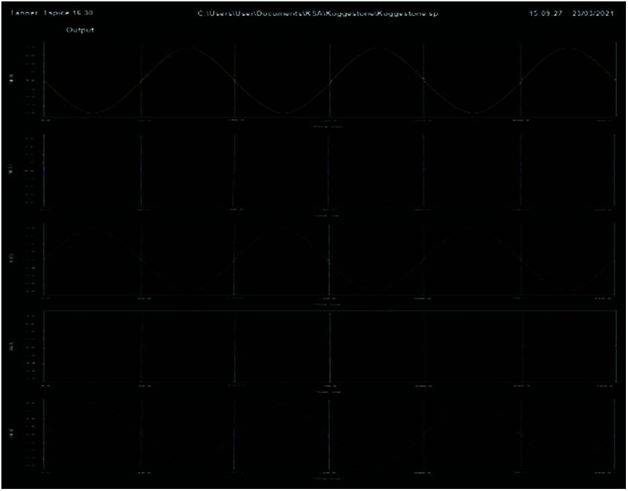
Figure 9: Output waveform of ECRL based kogge-stone circuit using CLAA
3.3 Kogge-Stone Using Multiplexer
Propagation delays in the circuits can be further reduced by implementing multiplexers in the circuit. The complexity that goes into designing each logic gate can be efficiently suppressed by employing 2-1 multiplexers. MUX benefits from universal gate status, as any kind of gate can be executed using this. When provided with real and inverted inputs, it produces both real and inverted outputs. In the above circuit, the XOR gate at the final stage has been replaced with a 2-1 MUX, shown in Figs. 10 and 11 shows the Transient characteristics of the Kogge-stone adder implemented using 2:1 Multiplexers.
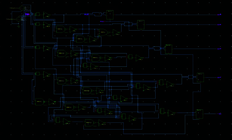
Figure 10: ECRL based kogge-stone circuit of CLAA, implemented using 2-1 MUX
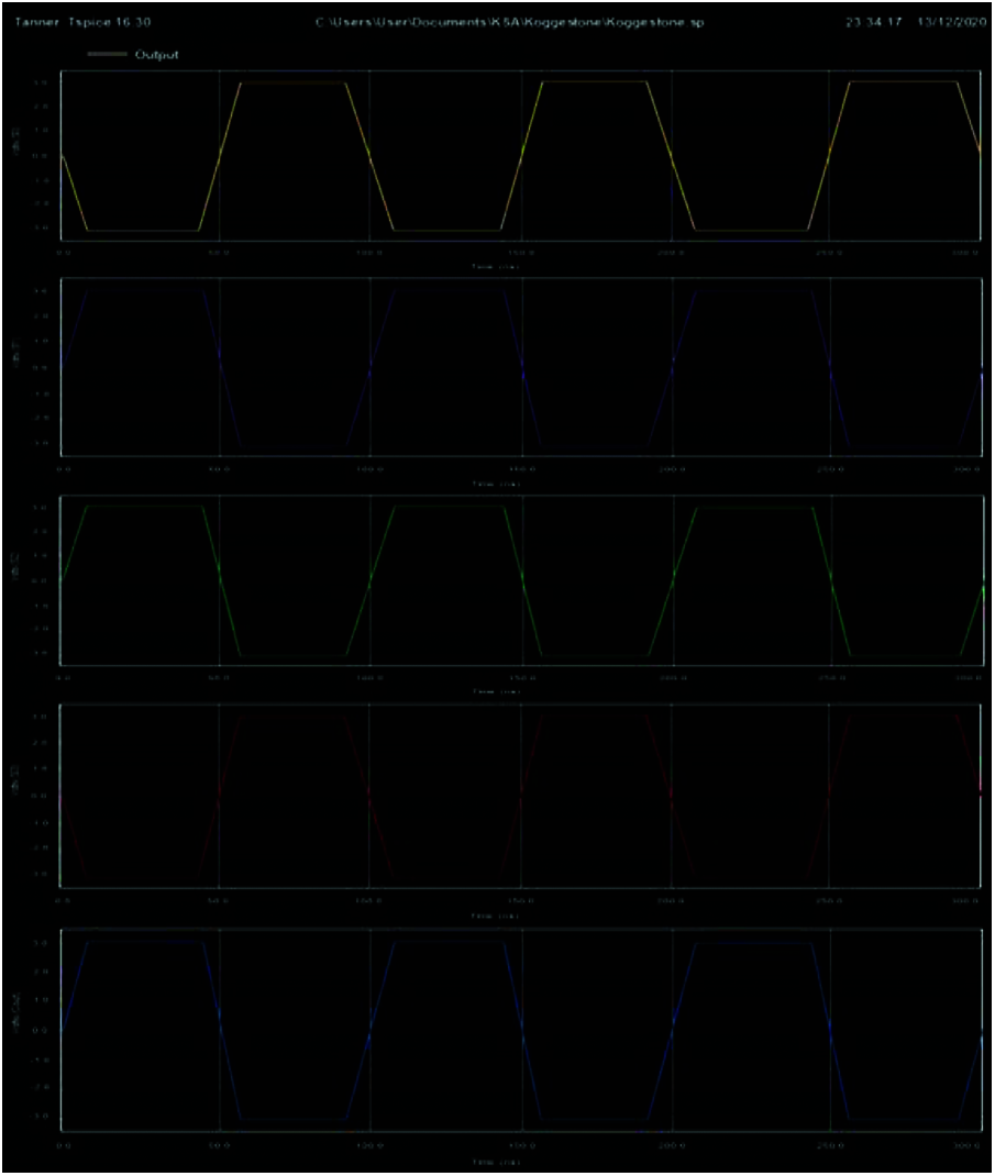
Figure 11: Transient characteristics of the ECRL based kogge-stone adder using multiplexers
3.4 FFT Implementation Using Kogge-Stone Adder
The Finite Fourier Transform (FFT) is implemented using the KSA with the help of a radix 4 SDF as explained in Section 3. The developed circuit of the FFT using the ECRL based Kogge-stone adder is given in Figs. 12 and 13 shows the performance analysis of the FFT system in terms of x0, x1, x2 and x3.
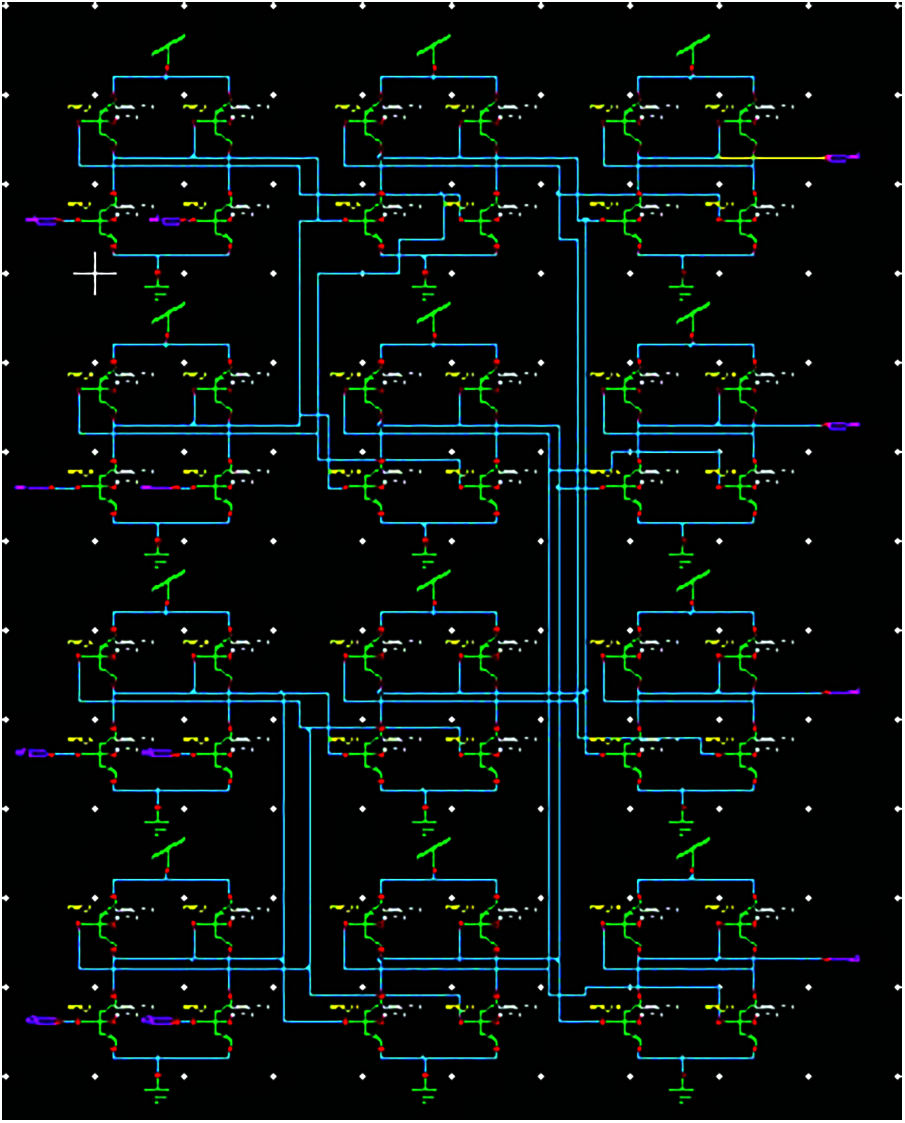
Figure 12: Radix 4 SDF implementation of FFT using ECRL-based kogge-stone adder
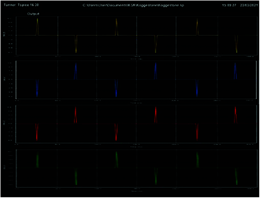
Figure 13: Performance analysis of FFT system built using ECRL-based KSA circuit
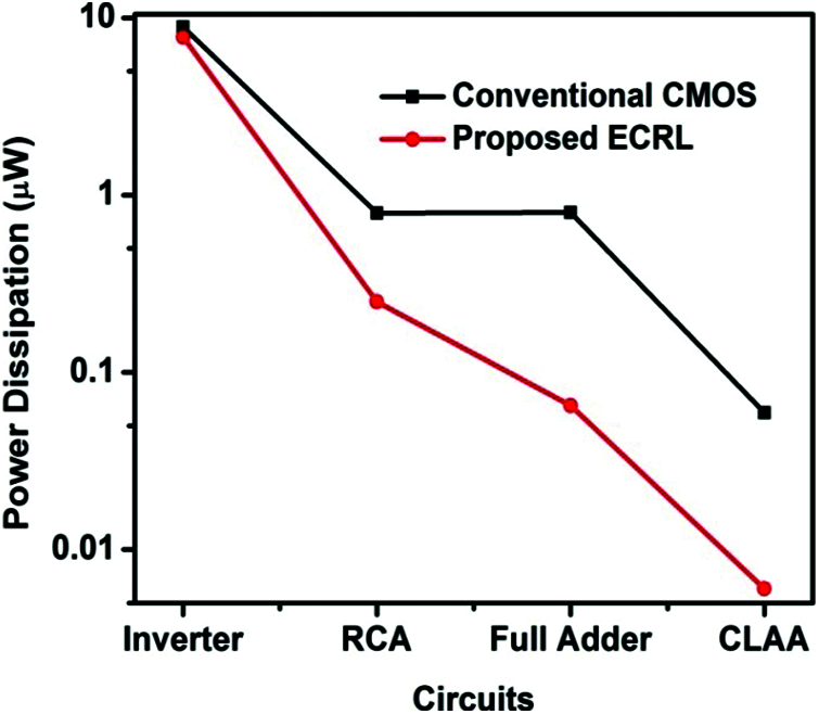
Figure 14: Graphical representation of the power dissipation of several circuits built using the proposed ECRL and conventional CMOS logic
Tab. 1 displays the various power dissipation values for the ECRL based proposed device when compared with several other circuits from the literature. It is shown at the bottom of the table that the ECRL logic implemented for the Carry Look-ahead adder yielded power dissipation as low as 6.0038 nW. Tab. 2 shows the number of transistors used for designing the ECRL based Kogge-Stone circuit and the number of load capacitors used. Tab. 3 shows the propagation delays of several circuits designed using ECRL compared with the traditional CMOS based circuits.
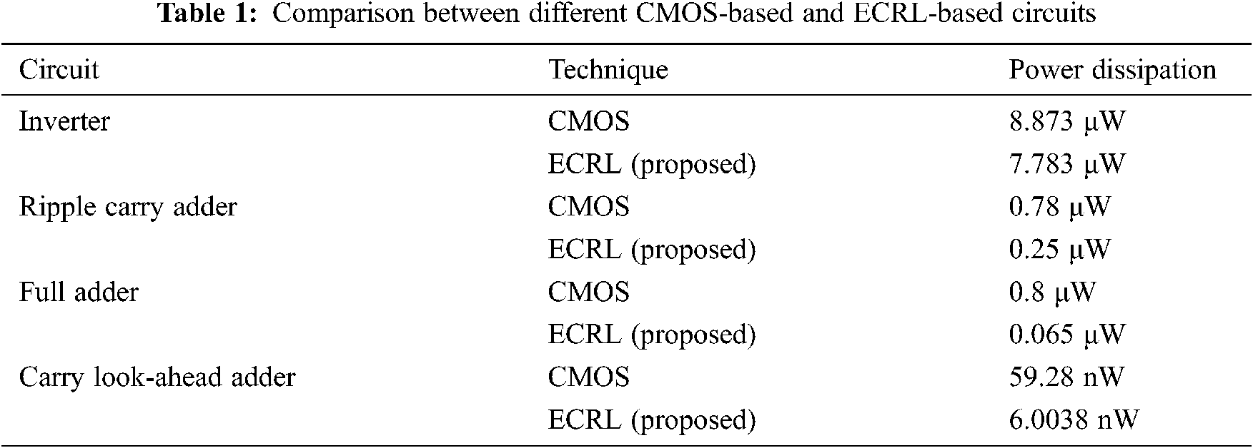
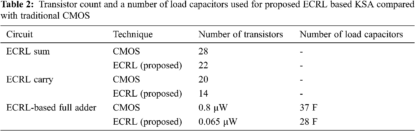
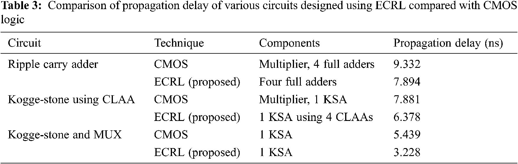
Fig. 14 shows the dissipation of various circuits built using ECRL compared to the proposed ECRL technique. The Carry Look-ahead Adder for the proposed ECRL technique shows a minimum power dissipation value of 6 nW.
This paper reports on the energy conservation of ECRL-based Kogge-stone adder circuits for DSP applications like Fast Fourier Transform (FFT). By utilizing minimum transistors and designing full adder and Carry Look-Ahead adder circuits using ECR logic, a reduced power dissipation was obtained in the range of nanowatts (nW). This adiabatic technology employs recharging functionality and develops an effective power dissipation factor. This methodology decreases the propagation delay in fast switching circuits, as a result of which the device becomes even cost economic. A multiplexer is also designed with the carry look-ahead adder, which benefits from variable adder length, making the number of multiplexer stages to a minimum. Comparison is performed for the proposed inverter, ripple carry adder, full adder and carry look-ahead adders with their corresponding CMOS based circuits. The comparison depicted a much-reduced power dissipation from the adiabatic logic, which makes it a compatible device and core contender for high-performance DSP applications like modem concentrators, cellular base stations etc. A Finite Fourier Transform (FFT) architecture is constructed using the KSA structure with the help of a Radix 4 format. Minimal power dissipation of 6.0038 nW is attained for the proposed design with a reduced propagation delay of around 3 ns.
Funding Statement: The authors received no specific funding for this study.
Conflicts of Interest: The authors declare that they have no conflicts of interest to report regarding the present study.
1. P. Ghosh, T. Saha and B. Kumari, “Aspects of low-power high-speed CMOS VLSI design: A review,” Industry Interactive Innovations in Science, Engineering and Technology, vol. 12, no. 2, pp. 385–394, 2018. [Google Scholar]
2. S. M. Kang and Y. Leblebici, “CMOS digital integrated circuits—Analysis and design,” Third Edition, McGraw-Hill, Newyork, USA, 2003. [Google Scholar]
3. W. C. Athas, W. C. Koller and L. J. Svensson, “An energy efficient CMOS line driver using adiabatic switching,” in Proc. of Fourth Great Lakes Symposium on VLSI, California, pp. 196–199, 2005. [Google Scholar]
4. J. Fischer, E. Amirante, A. B. Stoffi and D. S. Landsiedel, “Improving the positive feedback adiabatic logic family,” Advances in Radio Science, vol. 2, no. 1, pp. 221–225, 2005. [Google Scholar]
5. A. Blotti, M. Castellucci and R. Saletti, “Designing carry look-ahead adders with an adiabatic logic standard-cell library,” in Proc. Int. Workshop on Power and Timing Modeling, Optimization and Simulation, Springer, Berlin, Heidelberg, pp. 118–127, 2002. [Google Scholar]
6. M. Alioto and G. Palumbo, “Analysis and comparison on full adder block in submicron technology,” IEEE Transactions on Very Large Scale Integration (VLSI) Systems, vol. 10, no. 6, pp. 806–823, 2002. [Google Scholar]
7. N. Anuar, Y. Takahashi and T. Sekine, “Two phase clocked adiabatic static CMOS logic and its logic family,” Journal of Semiconductor Technology and Science, vol. 10, no. 1, pp. 1–10, 2010. [Google Scholar]
8. A. K. Bakshi and M. Sharma, “Design of basic gates using ECRL and PFAL,” in Proc.Int. Conf. on Advances in Computing, Communications and Informatics (ICACCIMysore, India, pp. 580–585, 2013. [Google Scholar]
9. P. Teichmann, “Adiabatic logic, future trend and system level perspective,” Springer Science & Business Media, vol. 34, no. 12, pp. 166–178, 2012. [Google Scholar]
10. M. A. Chowdhury, M. S. Rizwana and M. S. Islam, “An efficient VLSI design approach to reduce static power using variable body biasing,” World Academy of Science, Engineering and Technology, vol. 64, no. 2, pp. 7–15, 2012. [Google Scholar]
11. S. H. Kim and V. J. Mooney, “Sleepy keeper: A new approach to low-leakage power VLSI design,” in IFIP Int. Conf. on Very Large Scale Integration, Nice, France, pp. 367–372, 2006. [Google Scholar]
12. W. C. Athas, L. J. Svensson, J. G. Koller, N. Tzartzanis and E. Y. Chou, “Low-power digital systems based on adiabatic-switching principles,” IEEE Transactions on Very Large Scale Integration (VLSI) Systems, vol. 2, no. 04, pp. 328–407, 1994. [Google Scholar]
13. A. Chandrakasan, S. Sheng and R. W. Brodersen, “Low-power CMOS digital design,” IEEE Journal of Solid State Circuits, vol. 27, no. 4, pp. 473–484, 1992. [Google Scholar]
14. N. Zhuang and H. Whu, “A new design of the CMOS full adder,” IEEE Journal of Solid State Circuits, vol. 27, no. 5, pp. 840–844, 1992. [Google Scholar]
15. K. Navi, M. R. Saatchi and O. Daei, “A high-speed hybrid full adder,” European Journal of Scientific Research, vol. 26, no. 1, pp. 29–33, 2009. [Google Scholar]
16. R. K. Yadav, A. K. Rana, S. Chauhan, D. Ranka and K. Yadav, “Adiabatic technique for energy efficient logic circuits design,” in Int. Conf. on Emerging Trends in Electrical and Computer Technology, Nagercoil, India, pp. 776–780, 2011. [Google Scholar]
17. S. Kim, C. H. Ziesler and M. C. Papaefthymiou, “Charge-recovery computing on silicon,” IEEE Transactions on. Computers, vol. 54, no. 6, pp. 651–659, 2005. [Google Scholar]
18. E. S. Chew, M. W. Phyu and W. L. Goh, “Ultra low-power full-adder for biomedical applications,” in IEEE International Conference of Electron Devices and Solid-State Circuits (EDSSCXi’an, China, pp. 115–118, 2009. [Google Scholar]
19. C. H. Chang, J. Gu and M. Zhang, “A review of 0.18-/spl mu/m full adder performances for tree structured arithmetic circuits,” IEEE Transactions on Very Large Scale Integration (VLSI) Systems, vol. 13, no. 6, pp. 686–695, 2005. [Google Scholar]
20. S. Goel, A. Kumar and M. A. Bayoumi, “Design of robust, energy-efficient full adders for deep-submicrometer design using hybrid-cMOS logic style,” IEEE Transactions on Very Large Scale Integration (VLSI) Systems, vol. 14, no. 12, pp. 1309–1321, 2006. [Google Scholar]
21. K. Dhireesha and E. John, “Implementation of low power digital multipliers using 10 transistor adder blocks,” Journal of Low Power Electron, vol. 1, no. 3, pp. 1–11, 2005. [Google Scholar]
22. M. Alioto and G. Palumbo, “Performance evaluation of adiabatic gates,” IEEE Transactions on Circuits and Systems I: Fundamental Theory and Applications, vol. 47, no. 9, pp. 1297–1308, 2000. [Google Scholar]
23. A. Blotti, S. D. Pascoli and R. A. Saletti, “Comparison of some circuit schemes for semi-reversible adiabatic logic,” International Journal of Electronics, vol. 89, no. 2, pp. 147–158, 2002. [Google Scholar]
24. B. Patel and P. Kadam, “Comparative analysis of adiabatic logic techniques,” International Journal of Computer Applications, vol. 3, no. 4, pp. 975–984, 2015. [Google Scholar]
25. P. Sasipriya and V. K. Bhaaskaran, “Two phase sinusoidal power clocked quasi-static adiabatic logic families,” in Proc. Eighth Int. Conf. on Contemporary Computing (IC3Noida, India, pp. 503–508, 2015. [Google Scholar]
26. S. Amalin Marina, T. S. Pradeepa and A. Rajeswari, “Analysis of full adder using adiabatic charge recovery logic,” in Int. Conf. on Circuit, Power and Computing Technologies(ICCPCTNagercoil, India, pp. 1–6, 2016. [Google Scholar]
27. B. Rajesh, S. Nagraj and M. K. Chaitanya, “Full adder using CMOS technology,” International Journal of Advanced Trends in Engineering, Science and Technology, vol. 4, no. 1, pp. 208–211, 2016. [Google Scholar]
28. S. Archana and G. Durga, “Design of low power and high speed ripple carry adder,” in Proc. Int. Conf. on Communication and Signal Processing, Melmaruvathur, India, pp. 939–943, 2014. [Google Scholar]
29. V. Galphat and N. Lonbale, “The high speed multiplier by using prefix adder with MUX and vedic multiplication,” International Journal of Science and Research (IJSR), vol. 5, no. 1, pp. 2319–7064, 2016. [Google Scholar]
 | This work is licensed under a Creative Commons Attribution 4.0 International License, which permits unrestricted use, distribution, and reproduction in any medium, provided the original work is properly cited. |