DOI:10.32604/iasc.2022.023284
| Intelligent Automation & Soft Computing DOI:10.32604/iasc.2022.023284 | |
| Article |
Design of Logically Obfuscated Memory and Arithmetic Logic Unit for Improved Hardware Security
1Department of Electronics and Communication Engineering, Velammal Engineering College, Chennai, Tamilnadu, 600040, India
2Department of Electronics and Communication Engineering, Madurai Institute of Engg and Technology, Sivagangai, Tamilnadu, 630611, India
3Department of Electronics and Communication Engineering, Erode Sengunthar Engineering College, Erode, Tamilnadu, 638057, India
4Department of Electronics and Communication Engineering, PSR Engineering College, Sivakasi, Tamilnadu, 626140, India
*Corresponding Author: M. Usharani. Email: usharaniphd@gmail.com
Received: 01 September 2021; Accepted: 11 October 2021
Abstract: In any kind of digital system, the processor and memories are used to play a vital role in today’s trend. The processors and memories are done many critical tasks in the system. Whereas the processor used to do several functions and memories used to store and retrieve the data. But these processors and memories are more vulnerable to various hardware attacks. By using several new devices may lead to many security issues which the attackers can leverage to introduce a new hardware attack. Various hardware security (HS) studies have been presented to prevent hardware from a security issue. Some of the security issues that are occurred in hardware are overbuilding, piracy and reverse engineering (RE) and so on. In many works of literature, obfuscating and camouflaging are done in the netlist of hardware devices. Even though, these methods are highly overheads, and also not secured up to the level of expectation. Therefore, the main motive of Hardware security is to secure an Arithmetic Logic Unit (ALU) processor and memory unit from the various threats. In this work, a Configurable GDI based Locking cell (GLC) is proposed which is added as redundant to the original netlist of ALU and memory units for its hardware protection. The basic concept of configurable GLC is to perform a wire or inverter by using keys to obfuscate an attacker. This GLC logic can overcome the drawback of existing methods based on obfuscation and cryptographic techniques. The results show that proposed GLC is possible in any kind of memory system, all with low area and delay penalty.
Keywords: Hardware security; GLC; ALU; attacker; memory
Hardware is the base and the source of trust for any system security. With the rapid technological development of embedded organizations which can also provide hardware attacks threats on immense in nature [1]. In recent times, there are numerous software-based security systems are switched to Hardware-based security (HS) solutions for improving the system’s reliability. This security concern is provided in all systems from smartcards devices to all the military electronic systems.
Therefore, it is necessary to improve the hardware devices security to overcome the present thwarting issues like reverse engineering (RE), hardware fault injections attack or side-channel attacks and so on [2]. The main objective of HS is done for the protection and maintenance of system data from third parties or attackers. Some of the traditional methods that are followed for HS are Watermarking, Fingerprinting, patents, Trademarks, Radio-frequency identification (RFID), Cryptographic method and obfuscation techniques etc.
Several methods are used for the HS which is not defending up to the level of satisfaction. A few techniques like Logic Encryption and obfuscation to be replaced the prior concepts of HS which is better than the prior concepts. Therefore, this work is also focused on the area, security and power overhead on proposing the logic of Gate Diffusion Input (GDI) cell for an HS.
In this work, the GDI logic is implemented for the security of ALU processor and memory in the system. The ALU processor is a significant part of a computer system that is used to perform all the arithmetic, logical, control and input/output (I/O) operations. These operations should be highly secured to perform an exact output to achieve reliability but this processor is also threatened by attackers. Also, the memory unit is the most important device for storing the data. This memory has both ROM and RAM which is in need to perform an encryption and decryption technique to prevent the data.
Therefore, to maintain the security of ALU and memory unit, in this work, a configurable GDI based Locking Cell (GLC) is presented for both memory and ALU protection. This technique is compared with the previous obfuscation methodology to justify the reliability and security of this work.
The rest of the paper is organized as follow: Section 2 is described the security challenges that are faced by the HS and in Section 3, the related work of the proposed obfuscation is presented in it. The preliminaries based on the GDI gates are discussed in Section 3 and in Section 4, the proposed methodology is explained with an architecture. Section 5 showed the results and the discussion with the prior method comparison and finally, this work is concluded with Section 6 and the references.
The electronic IC manufacturing industries have specific constraints based on the low-cost design and high profit in the trade [3]. Even though the security is based on the additional attachments to the original circuit devices which has increased the circuit’s area. But the field is very worse without the security so that several challenges are faced by the HS which is given in the following.
The fingerprinting system is a method that is used for authentication which can protect intellectual property (IP) cores against Reverse Engineering (RE) [1]. This system is done for privacy where the IP is accessed only by an authorized user.
In some of the research, the Physical Unclonable Function (PUF) is used for an authentication process [4]. The challenge-response pair protocols are confirmed between the manufacturer and end-users which has been limited to the device utilities to the authentic user. However, PUF-based authentication is obtained by the modelling attack method which is used to predict the PUF responses [3].
Camouflaging [5] is a method that is used to hide some circuit layout-level which is based on obfuscation. This type of prevention is difficult to retrieve the data through RE [5]. However, in the CMOS, the camouflaging gate diminishes the attacker’s strategy and achieves protection. Several strategies are based on Design-level obfuscation which is also a logic encryption method that could prevent the data from data recovering without a key [6]. This method is stronger and reliable to an attack. The attackers can only access if both netlist and the keys are known.
Counterfeit ICs is a technique that is to be remarked, recycled, cloned, overproduced, tampered or out-of-spec IC which is mostly used for military applications [7]. The PUFs and ageing sensors are the solutions that are used to detect counterfeit products. Similarly, this method has high-power utility and area costs. The attacks like side-channel analysis and fault injections, Cryptographic circuits are also cannot defend the power supply-based fault injections. In order to prevent the side-channel attack, the numerous on-chip sensors and logic circuits. Therefore, to face these kinds of challenges, the researchers need to focus on some novelty in the upcoming technologies.
In this section, several works are presented in HS based on the memory and ALU of the system. This section gathers an idea of many pieces of literatures for the purpose of enhancing proposed system security.
Xie et al. [8] provided security in the 64 Kb RAM on the basis of resisting invasive attacks. Some of the invasive attacks are resisting timing channel (RTC) attacks, de-processing and observation of microscopy. This system is used for the protection to write with feedback and also the logic platform integration. Another work presented by Zhang et al. [9] discussed about the Random bit generation of memory in non-volatility memories. This method performs a random bit output without disturbing the stored data.
The method of sneak-path encryption (SPE) is developed by Kannan et al. [10] which is based on the data protection in non-volatile main memories NVMMs. This method is independent of instruction set which is dependent on hardware encryption and also it has a minimal performance impact. Swami et al. [11] presented an HS architecture which is named as Architecture for Secure Non-Volatile Memories (ARSENAL). The method of Smart Writes for Faster Transactions (SWIFT) technique is used in atomic security meta-data updates on every write-back for reducing the overhead of performance. The technique based on memory protection is called Mimosa which is used for RSA private keys protection from physical memory attacks. This Mimosa technique is an idle memory that is encrypted as ciphertext and developed by Guan et al. [12].
Saravanan et al. [13] discussed an ALU based logic encryption method by ensuring correct functionality simultaneously. This method has a higher efficiency which is suited for a recent cryptosystem. The outcome showed that the obfuscation module presence is achieved without increasing ALU’s area and power overhead. A functional obfuscation technique that is used to perform a modification in the gate-level functions is presented. It considered the number of inputs, number of gates and the number of outputs that are used for a signature generation which is developed by Reddy et al. [14]. Therefore, not all the inputs are utilized in overall circuits so that all the unused inputs are framed as a sub-circuit module function to reduce the area and also obtain the security of a processor. These methods are efficient in security to confuse attackers which are complex to identify a circuit functionality which is presented by Chandini et al. [15].
Lao et al. [16] performed logic locking (LL) techniques for digital signal processing applications which is inspired from the cyber security competitions. This method addressed a community-driven benchmarking that is used to provide a “snapshot” of the current field which wider a lesson for HS benchmarking. Huu et al. [17] presented a fault-tolerant system for ALU security. This system is focused on the time redundancy (TR) on performing three stages namely (i) Idle Time (IT) is used to operate a processor for the purposes of memory/register data dependency and cache miss etc, and IT does not need any additional time for interruption (ii) Idle Hardware (IH) has distinct Functional Units (FU) for several operations like an adder, subtractor, divider and multiplier. The recomputation performed simultaneously on the time of functions and Scheduling is also known as reordering for the purpose of execution. It is recomputed if IT or IH is required. These schemes are applied to protect the ALU processor.
This section carries a few ideas which are basic and also related to the proposed logic locking methodology. The basic structure of GDI and its function is discussed in this section.
Gate Diffusion Input (GDI) Technique
In this section, the GDI is discussed with detailed architecture and also its operation. The GDI is an advanced technique to achieve a low-power combinatorial circuit in the digital world. The GDI cell is similar to the Pass Transistor Logic (PTL) that is validated equally to Complementary Metal Oxide Semiconductor (CMOS) technology. This GDI is varied from the CMOS by providing a supply to the input terminals. The design complexity of an obfuscation cell (OC) is based on the area, power dissipation and delay which is a primary issue of OC. To overcome these issues the GDI technique is developed which is a simple concept in design and easily reduces the power consumption and are overhead. This technique on comparison with the existing logic styles of CMOS [18] and PTL [19]. Therefore, the GDI technique consists of only two transistors which are easy for the faster design and also obtaining a low-power than the CMOS and PTL.
The simple construction of the GDI cell is given in Fig. 1 which is remained the elementary structure of the CMOS inverter. However, the GDI has some of the special features that differ from the CMOS that is explained in the following.
1) This GDI cell comprises three inputs namely ‘G’ that indicate common input gates of pMOS and nMOS, ‘P’ is the pMOS source/drain input and then ‘N’ is the nMOS source/drain input.
2) The nMOS and pMOS Substances of both are interconnected to N or P respectively.
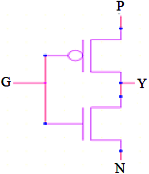
Figure 1: GDI cell
From Fig. 1, the GDI consists of three terminals i.e., N, P and G which is also associated with a VDD supply. This supply might be given to the input signal or can be grounded if decided according to the circuit design. Hence, the logic gates of AND, OR, XOR, MUX and so on are utilized based on the GDI which efficiently reduces the area based on the number of transistors. A few advantages of GDI cells over CMOS design are 1) low power dissipation and small delay obtained by reducing the number of transistors. 2) On minimizing the number of transistors which is obtained a minimum area and lesser interconnect effects which means reducing the circuit complexity.
Therefore, the simple GDI cell of input configuration that is related to the different boolean operations is tabulated in Tab. 1.
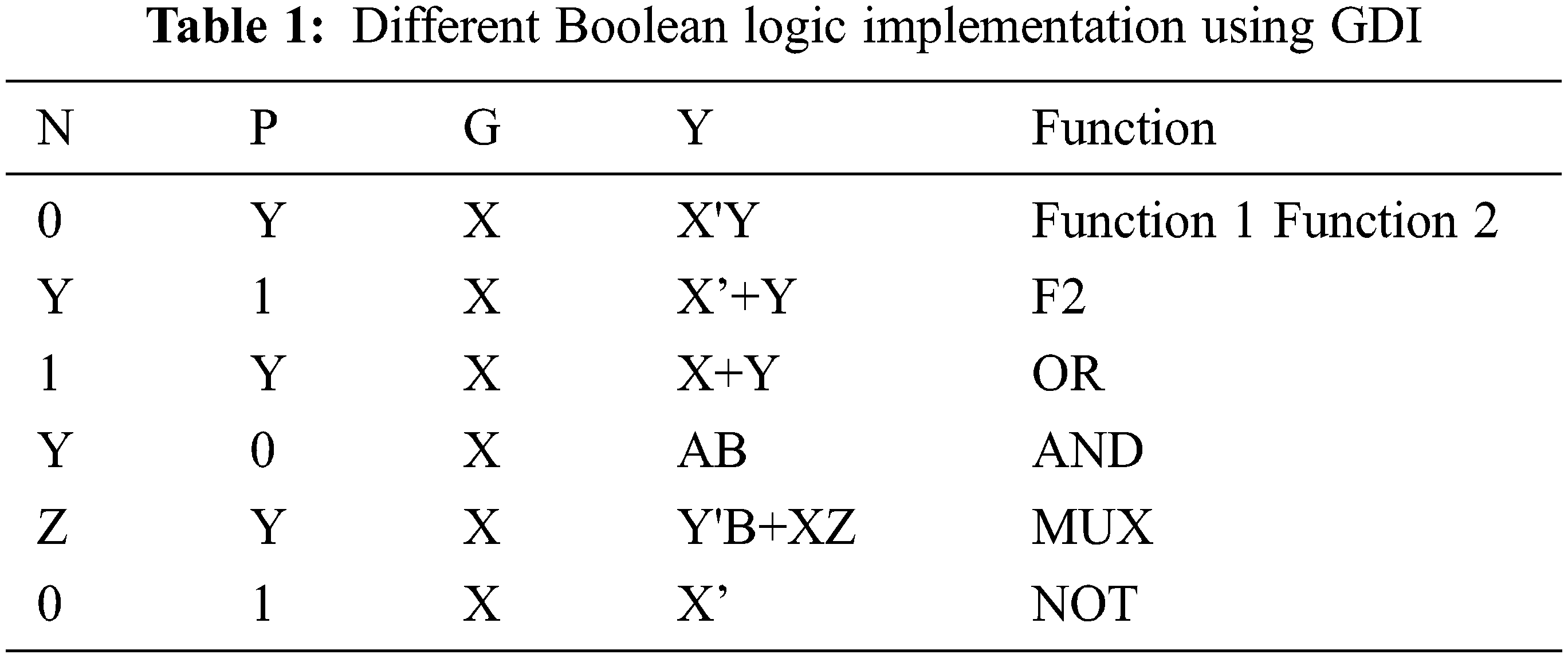
Form the above GDI function table, the GDI can able to perform all the function of logic gates and also the functions of MUX. Therefore, from the GDI functions, it is clear that the security of hardware can be easily performed by it. To prevent architecture of IC from the RE, overbuilding and piracy, the original design of circuit is modified with a logic locking based on GDI cell which is proposed in this work. Therefore, the obfuscation technique is used to modify the original circuits with the knowledge of key input. This obfuscated logic netlist is prevented from an attacker which is also implemented in all the hardware architecture for security.
In this section, the proposed methodology based on GDI based Locking Circuit (GLC) is presented. The basic function of proposed GLC is discussed and also it is applied to the both ALU and memory unit which is described in this section.
Proposed GLC
The proposed logic of GLC structure is given in Fig. 2 which consists of three terminals of input (in), input key of PMOS (kp) and an input key of NMOS (kn) respectively. In this logic, the function of GLC is to perform a configuration as an inverter or wire by using key values of kp and kn. To prevent the ALU and memory netlist from an attacker, this GLC is added as redundant to configure the function of exact netlist. However, When the input value of keys (kp, kn) is (1, 0), then the GLC is configured as an inverter. When the input value of (kp, kn) is (0, 1), then the GLC act as a wire. Therefore, the valid user can only access this system by using a correct key and get an output. By the configured netlist of ALU and memory using GLC is secured and protected from attackers and also the system’s reliability is increased.
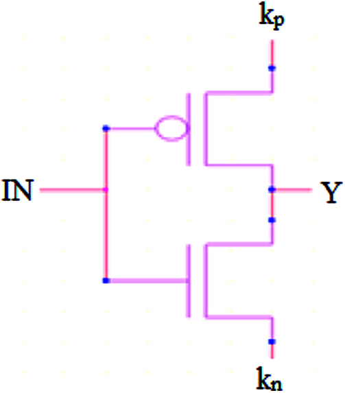
Figure 2: Proposed structure of GLC
Memory-based HS using GLC
Data protection from memory is not an easy process when it is damaged by an attack and also hard to recover. In order to maintain the HS of memory unit, the proposed GLC based encryption and decryption is done for data protection. This configurable GLC is performed in both the write and read operations of memory. The operation of encryption and decryption should process the same key to provide an exact output. Therefore, the output data is encrypted or configured when the memory is in a write operation. Similarly, the output function is decrypted or re-configured in the read operation by using the same correct keys. Figs. 3 and 4 shows proposed GLC based data encryption and decryption in memory. There is three main sections are presented that is encoder section, memory section and decoder section. The encoder section is used to perform a write operation which consists of CPU, data input and GLC respectively. Secondly, memory is the middle section of the proposed architecture where the encrypted data is used to store it. Finally, on the output side, the decoder section is connected for performing a read operation.
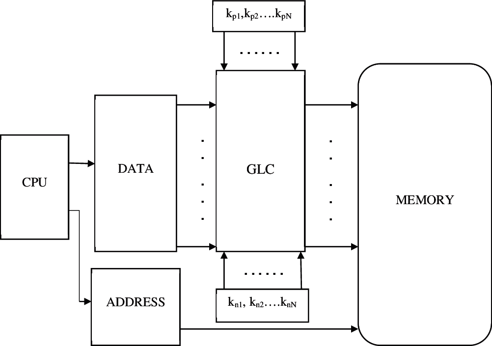
Figure 3: Encryption in memory using GLC
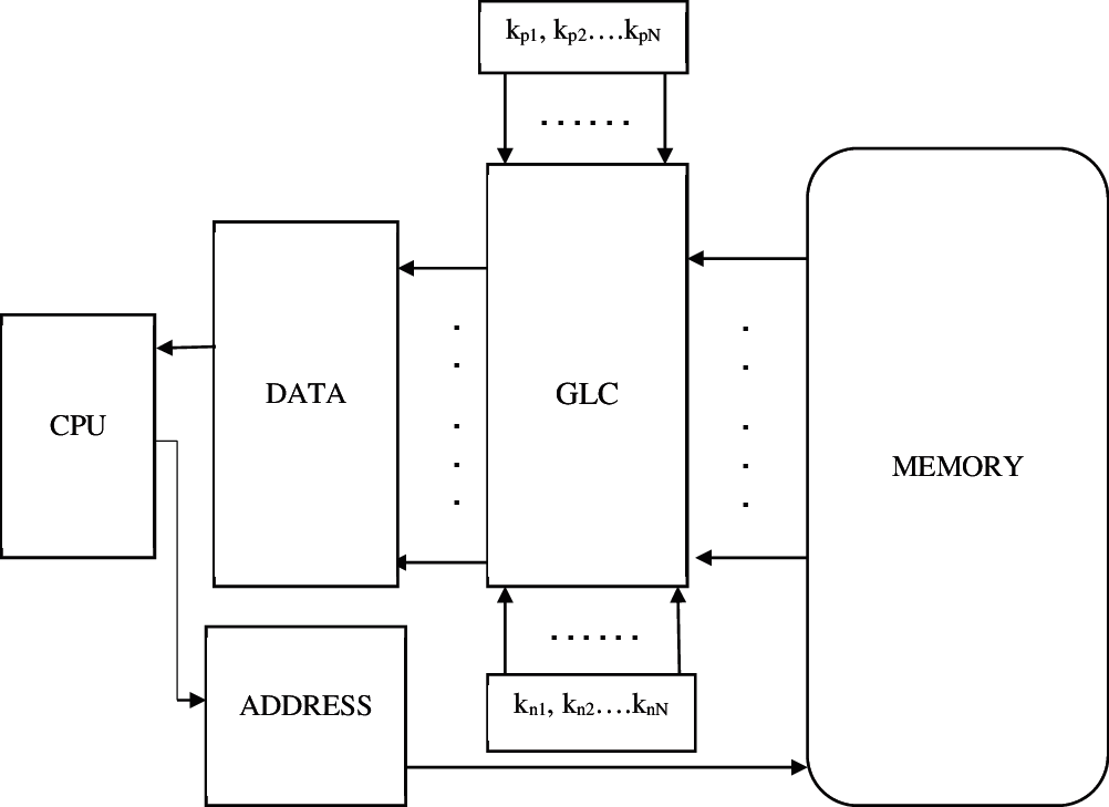
Figure 4: Decryption in memory using GLC
In the encoder section operation, n-bit data input from the CPU which is sent to the GLC block as input. The encoder side GLC has configured either inverter or wire based on the input keys. In Fig. 3, kp1, kp2….kpN and kn1, kn2….knN denotes key inputs of GLC for both P and N terminal denotes the number of rows or columns in memory. For example, by setting kp6 and kn6 as 01, the GLC is configured to behave as a wire, then, the inverted data is stored in memory. The original data only read from memory only by giving the correct key of kp6 and kn6 as 01 in the decoder side. N denotes the number of rows or columns in memory and then the encrypted data is stored in the memory section. After that, the read operation is carried out with the process of decryption. In the decoder section, the configurable GLC is the first function to perform decryption. The encrypted data of memory is entered as input to the decoder GLC block. If the same key is given for encoder GLC and decoder GLC, then the original data is provided as output. If the key of encoder GLC and decoder GLC is not similar, then the output is obfuscated.
ALU based HS using GLC
The ALU is a significant processor that has to be secured to perform all the functions. In this method, the ALU circuit is configured by inserting a proposed GLC into the design. The original functionality is hidden from an attacker by inserting GLC logic. Therefore the exact output is exposed only by applying the exact keys. The function of GLC based ALU is shown in Fig. 5.
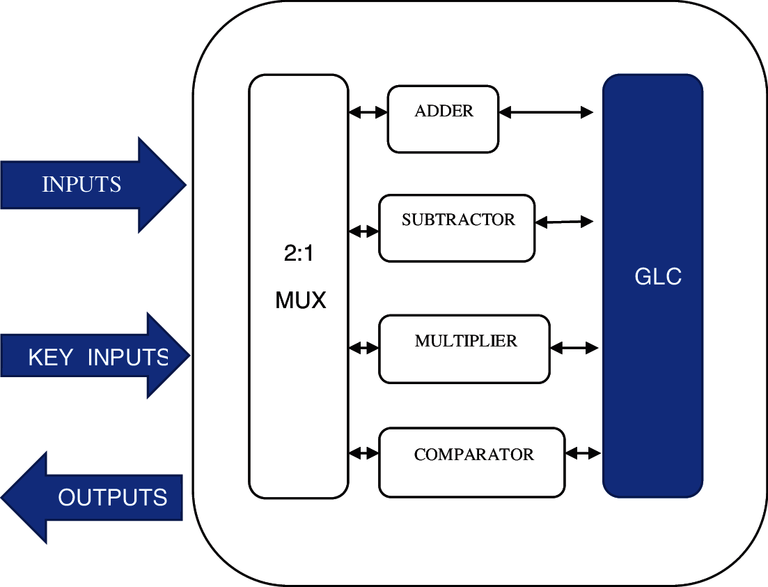
Figure 5: Proposed GLC based ALU
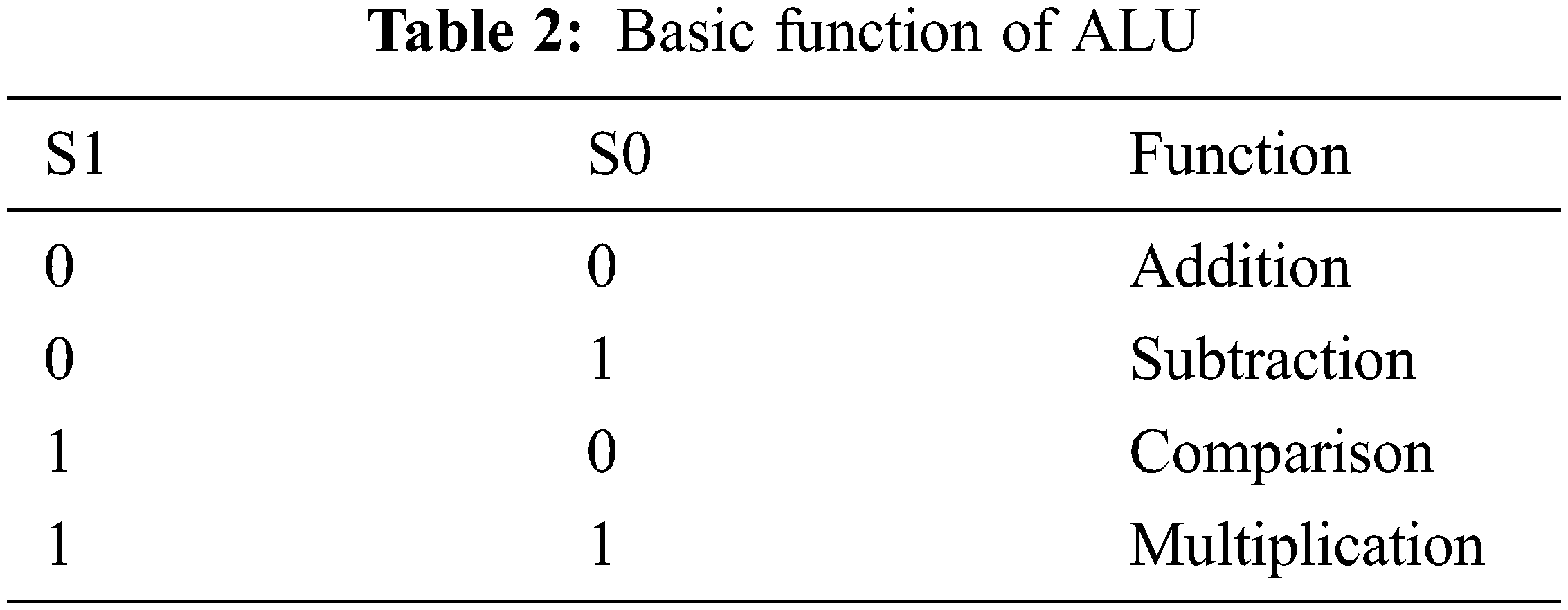
From Fig. 5, the proposed block consists of input, ALU block, GLC block and the output respectively. The n-bit input is given to the ALU block and this ALU unit is used to perform some arithmetic and logical functions based on selection keys S0 and S1 which is shown in Tab. 2. The exact output of ALU is sent into the GLC block for protection. The GLC block is configured based on the key values of k0 and k1. When the key k0 and k1 is 1 and 0, then the output is configured as an inverter. If the key k0 and k1 is 0 and 1, then the output acts as a wire. Therefore, the secured ALU is obtained with the logic of GLC which is more efficient than the previous technique.
The proposed memory and ALU protection technique are implemented using Cadence virtuoso schematic editor. To analyze the additional insertion overhead and effectiveness, the proposed protection technique compared with data scrambling based memory protection (R. Vijay Sai et al.) and sneak-path encryption (Sachhidh Kannan et al.) techniques. Tab. 3 shows the results of the implementation of 4 × 4 RAM with GLC.
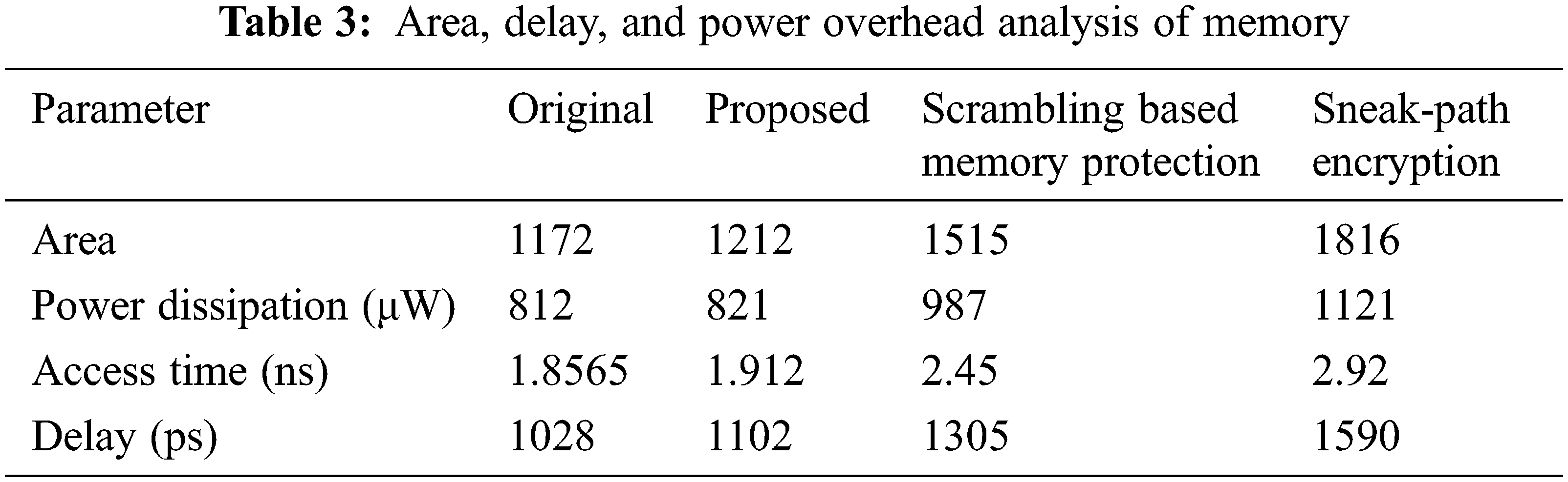
The area, power dissipation, access time and delay are estimated for original memory and memory with protection unit. Compared to other techniques, propose GLC method shows less area and power requirement in order to secure memory. Also, observed that area and power overhead, access time and delay due to GLC insertion are only on average 3.412%, 1.1%, 3% and 7.19%, respectively. The overhead analysis is graphically shown in Fig. 6.
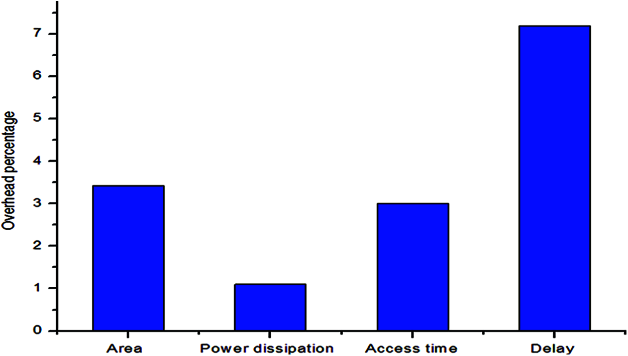
Figure 6: Overhead analysis of memory
Similarly, the area, power and delay analyzed for ALU for the proposed locking scheme and tabulated in Tab. 4. From the results observed that the area and power overhead and delay due to GLC insertion are only on average 6.36%, 7.969% and 7.769%, respectively. Fig. 7 show the overhead analysis of proposed ALU. The minimum insertion overhead of all parameters means that the proposed method in this brief can obfuscate the memory and ALU without any performance degradation.
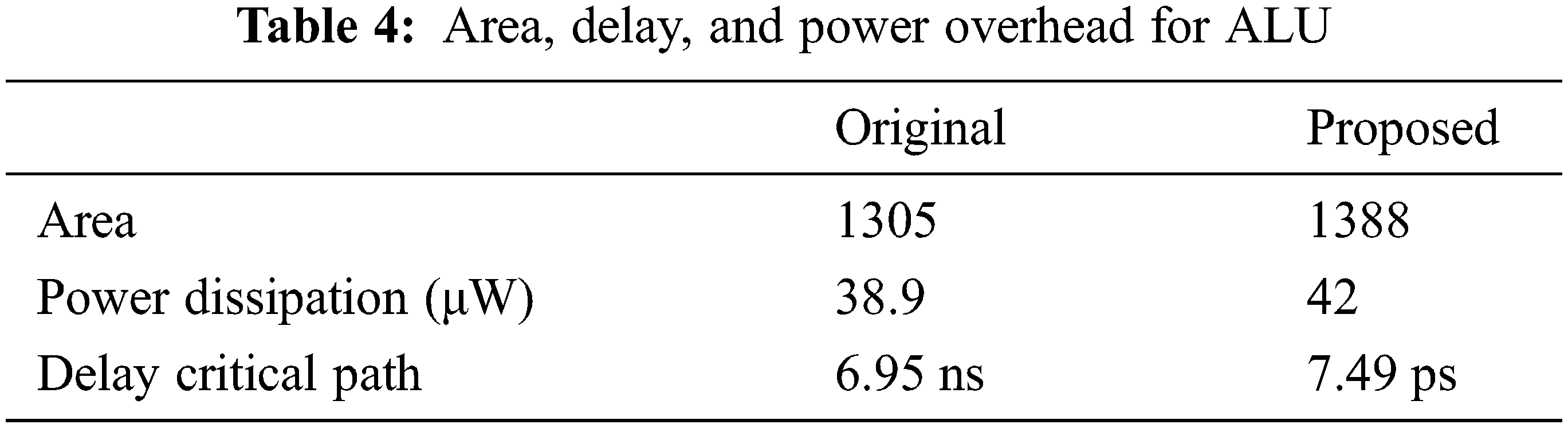
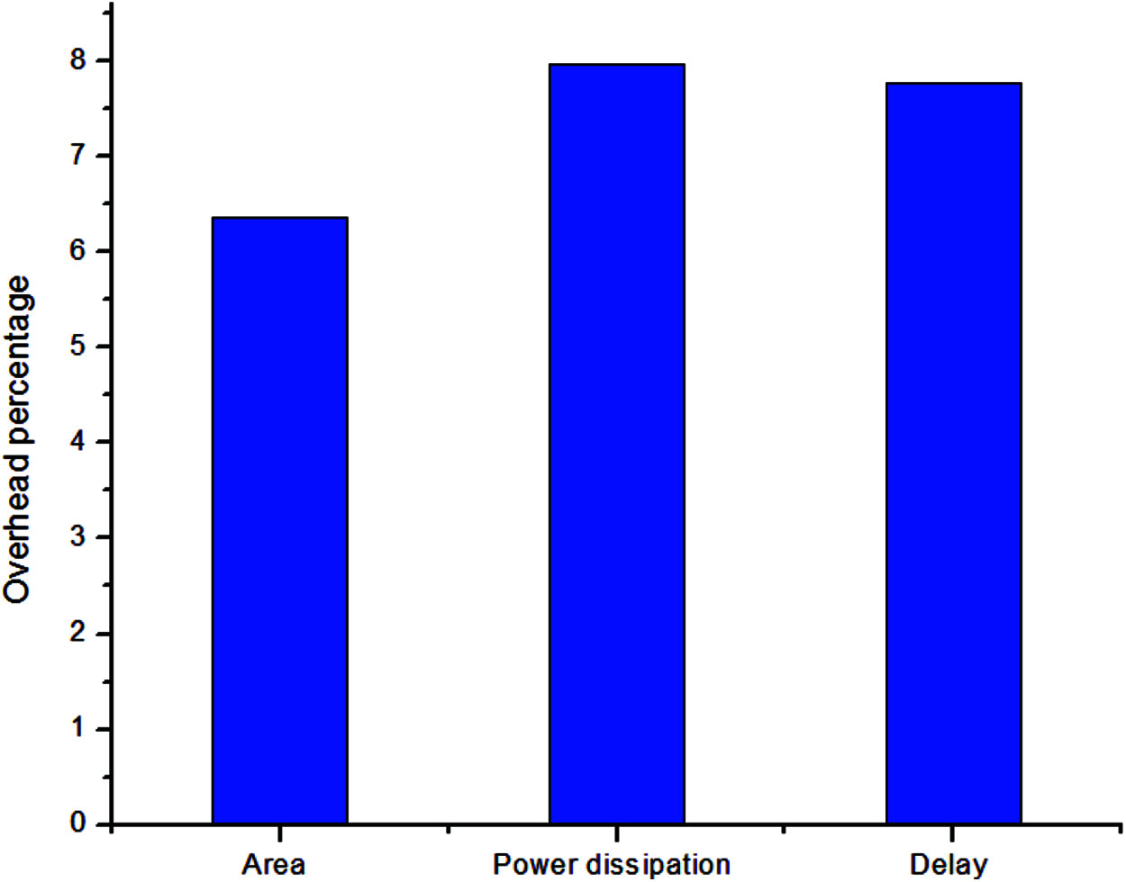
Figure 7: Overhead analysis of ALU
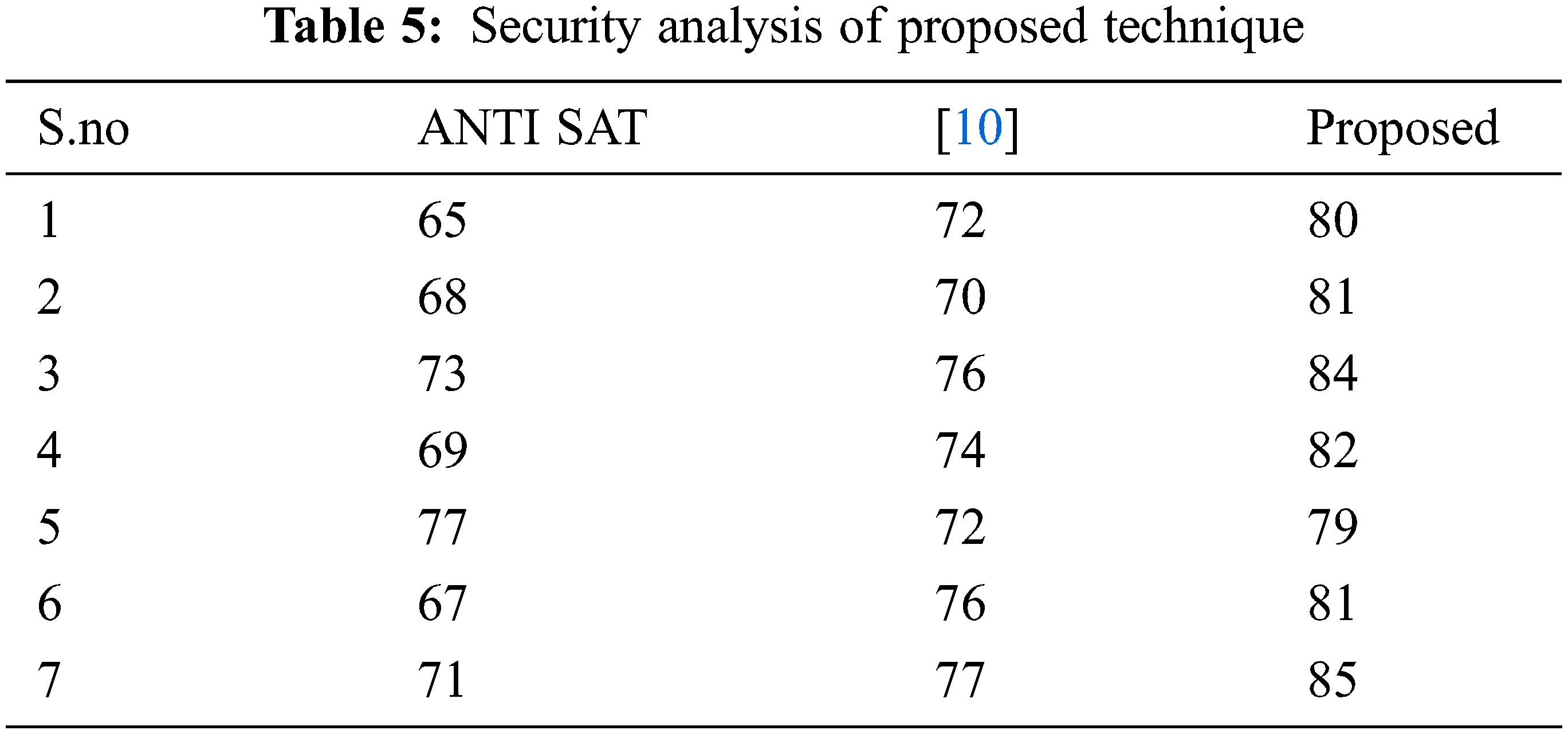
The security level is analyzed by performing read, write and satisfiability checking (SAT) attack iteration with the execution time to conclude the correct key. The processing unit time limit is set to 12 h. Tab. 5 shows average iterations needed to unlock the system by performing SAT attacking. From table observed that on average proposed technique requires more iterations to unlock a circuit.
In this work, the proposed GLC has presented hardware security for ALU and the memory unit of the system. This system achieved low power consumption and Low area overhead and also high security with a simple GDI logic. This method provides easy protection than the traditional methods. From the result, the proposed GLC technique is better than the prior method in all aspects. So that the HS of ALU and memory is improved efficiently and also the design implementation is also a simple process in this method. Therefore, the proposed methodology is most advanced to play a vital in future technology than any other HS technique.
Funding Statement: The authors received no specific funding for this study.
Conflicts of Interest: The authors declare that they have no conflicts of interest to report regarding the present study.
1. Y. Alkabani, F. Koushanfar and M. Potkonjak, “Remote activation of ICs for piracy prevention and digital right management,” in Proc. IEEE/ACM Int. Conf. Comput.-Aided Design, Rice University, USA, pp. 674–677, 2007. [Google Scholar]
2. M. Rostami, “Robust and reverse-engineering resilient PUF authentication and key-exchange by substring matching,” IEEE Transactions on Emerging Topics in Computing, vol. 2, no. 1, pp. 37–49, 2014. [Google Scholar]
3. U. R. Uhrmair, “Modeling attacks on physical unclonable functions,” in Proc. of the 17th ACM Conf. on Computer and Communications Security, ser. CCS ‘10, pp. 237–249, 2010. [Google Scholar]
4. J. A. Roy, F. Koushanfar and I. L. Markov, “EPIC: Ending piracy of integrated circuits,” in Proc. of Design and Automation and Test in Europe, Munich, Germany, pp. 1069–1074, 2008. [Google Scholar]
5. J. Rajendran, “Security analysis of integrated circuit camouflaging,” in Proc. of the 2013 ACM SIGSAC Conf. on Computer & Communications Security, ser. CCS ‘13, pp. 709–720, 2013. [Google Scholar]
6. J. Rajendran, “Fault analysis-based logic encryption,” IEEE Transactions on Computers, vol. 5, no. 6, pp. 99–103, 2013. [Google Scholar]
7. F. Koushanfar, “Provably secure active IC metering techniques for piracy avoidance and digital rights management,” IEEE Transaction on Information Forensics and Security, vol. 7, no. 1, pp. 51–63, 2012. [Google Scholar]
8. Y. Xie, X. Xue and J. Yang, “A logic resistive memory chip for embedded keys storage with physical security,” Transactions on Circuits and Systems II: Express Briefs, vol. 63, no. 4, pp. 336–340, 2016. [Google Scholar]
9. L. Zhang, X. Fon and C. H. Chang, “Optimizating emerging non-volatile memories for dual-mode applications: Data storage and Key generator,” IEEE Transactions on Computer-Aided Design of Integrated Circuits and Systems, vol. 34, no. 7, pp. 1176–1183, 2015. [Google Scholar]
10. S. Kannan and N. Karimi, “Security vulnerabilities of emerging nonvolatile main memories and countermeasures,” IEEE Transactions on Computer-Aided Design of Integrated Circuits and Systems, vol. 34, no. 1, pp. 2–5, 2015. [Google Scholar]
11. S. Swami and K. Mohanram, “ARSENAL: Architecture for secure non-volatile memories,” IEEE Computer Architecture Letters, vol. 17, no. 2, pp. 15–24, 2018. [Google Scholar]
12. L. Guan, J. Lin and B. Luo, “Protecting private keys against memory disclosure attacks using hardware transactional memory,” IEEE Symposium on Security and Privacy, San Jose, CA, USA, pp. 129–136, 2015. [Google Scholar]
13. K. Saravanan and N. Mohankumar, “Design of logically obfuscated n-bit ALU for enhanced security,” in 2019 3rd Int. Conf. on Electronics, Communication and Aerospace Technology (ICECA), Coimbatore, India, pp. 301–305, 2019. [Google Scholar]
14. D. M. Reddy, K. P. Akshay and R. Giridhar, “BHARKS: Built-in hardware authentication using random Key sequence,” in 4th Int. Conf. on Signal Processing, Computing and Control (ISPCC), Solan, India, pp. 200–204, 2017. [Google Scholar]
15. B. Chandini and M. Nirmala Devi, “Analysis of circuits for security using logic encryption,” In: Security in Computing and Communications. SSCC 2018. Communications in Computer and Information Science, vol. 9, no. 6, pp. 205–216, 2019. [Google Scholar]
16. Y. Lao and K. K. Parhi, “Obfuscating DSP circuits via high-level transformations,” IEEE Transaction on Very Large Scale Integration Systems, vol. 23, no. 5, pp. 819–830, 2015. [Google Scholar]
17. N. M. Huu, B. Robisson, M. Agoyan and N. Drach, “Low-cost fault tolerance on the ALU in simple pipelined processors,” in 13th IEEE Symp. on Design and Diagnostics of Electronic Circuits and Systems, Vienna, Austria, pp. 28–31, 2010. [Google Scholar]
18. S. F. Hsiao, M. Y. Tsai and C. S. Wen, “Low area/Power synthesis using hybrid pass transistor/CMOS logic cells in standard cell-based design environment,” IEEE Transactions on Circuits and Systems II: Express Briefs, vol. 57, no. 1, pp. 21–25, 2010. [Google Scholar]
19. A. Morgenshtein, A. Fish and I. A. Wagner, “Gate-diffusion input (GDIA power-efficient method for digital combinatorial circuits,” IEEE Transactions on Very Large Scale Integration (VLSI) Systems, vol. 10, no. 5, pp. 566–581, 2002. [Google Scholar]
 | This work is licensed under a Creative Commons Attribution 4.0 International License, which permits unrestricted use, distribution, and reproduction in any medium, provided the original work is properly cited. |