DOI:10.32604/iasc.2022.021984
| Intelligent Automation & Soft Computing DOI:10.32604/iasc.2022.021984 | |
| Article |
Field Programmable Gate Arrays (FPGA) Based Computational Complexity Analysis of Multicarrier Waveforms
1Department of ECE, University College of Engineering, Nagercoil, Tamilnadu, 629004, India
2Department of ECE, CSI Institute of Technology, Thovalai, Tamilnadu, 629302, India
*Corresponding Author: C. Ajitha. Email: ajitha14ucen@gmail.com
Received: 23 July 2021; Accepted: 16 September 2021
Abstract: Multicarrier waveforms with enhanced spectral efficiency, low latency, and high throughput are required for 5G wireless networks. The Orthogonal Frequency Division Multiplexing (OFDM) method is well-known in research, but due to its limited spectral efficiency, various alternative waveforms are being considered for 5G systems. In the recent communication world, NOMA (non-orthogonal multiple access) plays a significant part due to its wider transmission of data with less bandwidth allocation. Even if a high data rate can be attained, the transmission problem will arise due to the spread of multiple paths. In order to reduce complexity and area utilization, a novel PL-based FWFT (Fast walsh hadamard fourier transform) technique is proposed and implemented in the VLSI architecture. To achieve a high-performance system, the main concept of pass transistor logic (PL) with VLSI implementation is to diminish the size and power consumption. Finally, the performance of the proposed FWFT/ IFWFT implementation has been evaluated. For FPGA’s 16-point FWFT, the number of transistors decreased by 21% and the total power required was reduced by 5.5%. The same implementation for 34 transistor-pass-logic customs and power consumption is 2.764 mW with a latency of 78.256 ns. As a consequence, the proposed system achieves low power, area and low complexity system that can enhance the function of the multicarrier waveform systems.
Keywords: Fast walsh hadamard fourier transform; FPGA; pass logic transistor; multiple input multiple outputs
Wireless communication Beyond 5G (B5G) network goal is to enable many changes in the network related to quality and volume of the services such as low latency network communication [1], massive data transfer, augmented reality requires a more convenient network to perform this with more reliability. The Orthogonal Frequency Division Multiplexing (OFDM) method is well-known in research, but due to its limited spectral efficiency, various alternative waveforms which includes Filter Bank Multicarrier (FBMC) [2], Generalized Frequency Division Multiplexing (GFDM), Universal-Filtered Multicarrier (UFMC) and RB-adaptive F-OFDM [3]. To improve the spectral efficiency, Cyclic Prefix is inserted to the OFDM as (CP-OFDM), but FBMC can perform the transmission without CP. But the inter symbol interference makes the transmission signal to be attenuated, making it unsuitable for low latency states [4]. Although UFMC is considered for low latency scenarios, it’s out of band emission limited the transmission efficiency. The above multicarrier waveforms are elaborately listed below,
The notable CP-OFDM multicarrier waveform will be utilized without a doubt in future 5G advancements, since it gives great execution while keeping simplicity. The rule of OFDM is to separate the entire data transmission, so that channel adjustment can be regularly decreased [5]. In CP OFDM, the latter part of the OFDM frame’s data is added to the beginning of the OFDM frames to prevent inter-symbol interference (ISI) or inter-band interference in OFDM, and the length of the cyclic prefix should be higher than the channel delay spread. Furthermore, the channel delay spread varies with frequency, and the CP length should be broad enough to accommodate for both interferences and can be adaptable [6].
The transmission or else receipt part utilized in entire RBs is the identical, so it receipts advantage of existence modular and scalable. PTS and SLM are two roles included in the RB-F-OFDM framework [7] that help to reduce PAPR. The process of removing RB-F-OFDM enabled PAPR and increasing the efficiency of the provided device is known as phase rotation. Rayleigh’s distribution channel can be used to achieve a higher SNR value, resulting in improved system performance. The polyphase implementation of the IoT RB-F-OFDM system proposes a new transformation to minimize the PAPR and complexity. The system complexity in OFDM, FFT [8] is used because of IFFT at the transmitter and receiver, but this is condensed by FWFT and therefore decreases PAPR.
Channel bank-based waveforms don’t need cyclic prefix and accomplish great spectrum regulation and better side projection constrictions offering essentially improved capacities when managing the obstruction created by offbeat transmissions. In any case, the usage unpredictability of channel banks is higher than that of CP-OFDM frameworks [9]. FBMC subcarriers are ideally planned in the recurrence space to give spectrum conservativeness, these waveforms needn’t bother with a CP and accordingly are more spectrum effective. FBMC-QAM and FBMC-OQAM are the two option multicarrier waveforms dependent on the FBMC idea.
Generalized Frequency Division Multiplexing (GFDM) [10] is widespread with another idea and is made out of non-orthogonal subcarrier which spread the information as time and recurrence domain. In order to evade inter-symbol interference, a CP is added toward the termination of each square of images and gives a low latency signal on account of circular separating with model channels [11]. To improve the spectrum productivity, the tail biting method can be applied to diminish the CP length. To additionally progress the spectrum area, a windowing cycle can be included in the transmitter.
The UFMC waveform [12] is a subset of the OFDM waveform combined with post-separating, in which a group of transporters is sorted by utilizing a recurrence area proficient usage. Scientists are currently working on various plans [13] and experimenting with new waveforms [14]. UFMC conspire, that can overcome the constraints of OFDM, the speculation of OFDM and FBMC system is UFMC. It upholds low latency and quick time division duplex exchanging.
Due to its configurable circular shaping filters, NOMA [15] has taken abundant consideration in later scenery, versatility features such as small level OoB discharge, and its adaptability related to non-OFDM based waveforms [16]. NOMA can utilize non-contiguous spectrum chunks to transmit the signal through carrier aggregation techniques; but this is not possible for OFDM technique. In additional, NOMA is more spectral efficient and each block needed one CP and each block consists of many subcarriers and subblocks. Prototype filters are used to attract more NOMA features, requiring more hardware execution than OFDM. In order to ease the difficulty, low-complexity modulation/demodulation plans are quickly presented.
Another interesting technology for improving spectrum efficiency is cognitive radio (CR) [17]. The secondary user (SU) has access to the spectral range that is allocated to the primary user in CR (PU). As a result, cognitive NOMA anticipates more efficient spectrum allocation. The pairing of NOMA and CR is thought to be capable of enhancing spectrum efficiency even more (SE). Spectrum sharing has been extensively used because of its minimal complexity. It has been demonstrated that employing NOMA in CR improves SE substantially when contrasted to using OMA in CR. The functional differences of NOMA from OMA, the spectrum cannot be simultaneously accessed by users. In NOMA, multiple users can simultaneously access the available spectrum [18]. Therefore, NOMA is recognized as a strong campaigner among all other technologies because it has the important accent of overcoming the difficulties in OMA.
The complexity of the MIMO technique is another great real time problem. Thus, the complexity of this paper is concerned and reduced by the use of the FWFT algorithm. Instead of using FFT, here FWFT [19] is used because FWFT needs only fewer stages of multiplication compared with FFT which reduces the complexity and power consumption.
• FFT: For N subcarriers number of stages = N/2 log2 (N).
• FWFT: For N subcarriers number of stages = log2 (N)-1.
Basically, an IFWFT is a transform technique which is the pair of IDFT and IWHT. When compared IFFT, IFWFT has less complexity [20] and less resources. Ce Kang et al proposed an OFDM system with FWFT and PEC method to decrease the complexity range by using Piece-wise exponential companding, and the transform value is calculated based on fast wash- Hadamard function. Jinqi Liu et al proposed a pipeline structure for FWFT. In recent years FWFT is an important term to find the transform parameters. The planned architecture decreases the quantity of buffers by 50 percent and adders by 25 percent. But FWFT’s real time is not a satisfactory function, so FWFT is implemented in the VLSI structure to convert the system into a fixed real-time application. The achievement of high-performance multicarrier generation system, pass transistor logic (PL) based VLSI implementation is used to decrease the size and power consumption.
The rest of the paper is systematized as follows: Detailed literature of the FPGA-based NOMA system is described in Section 2. The proposed methodology of the novel FWFT method for the transmission of NOMA and the Pass Logic Circuit is described in Section 3. The implementation of hardware and FPGA can be discussed in Section 4. Experimental outcomes and complexity results have been simulated in Section 5. Finally, the conclusion arrived is presented in Section 6.
Chin-Teng Lin et al proposed a pipeline radix-
Kazuo Yano et al proposed a CPL to the whole dangerous track. The CPL comprises of CMOS, an NMOS pass-transistor rationale organize, and complementary inputs/outputs earns inverters. Basically, multiplication time is fastest method compared with other methods. Anbarasan et al explained OFDM applications using FFT processing and VLSI implementation and IFFT processors also reduce the power and chip area with the help of processing elements. Teng Su et al recommended the combined form about WHT and DFT into an on the single algorithm which is called as fast Hadamard–Fourier transforms algorithms. The algorithm produces the scant matrices for each step-in radix-R mode.
2.1 Existing Fast Fourier Transform Techniques
The reason why FWFT is used instead of FFT is, it uses only a few multiplication and addition stages. For instance, to compute a 16-point FFT, radix-4 proceeds only
• Number of stages required for complex multiplications (FFT) =
• Number of stages required for complex additions (FFT) =
• Number of complex multiplications (FWFT) =
• Number of complex additions (FWFT) =
In Fig. 1, 16-point radix 4 FFT has 32 complex multiplications and 64 complex additional stages. But the 16-point radix 4 FWFT uses 17 multiplication and 51 additional stages. As a result, the number of stages required for FWFT is very low compared to the number of stages used in FFT. Thus, the complexity range is reduced and implemented in VLSI to make this system a real-time application.
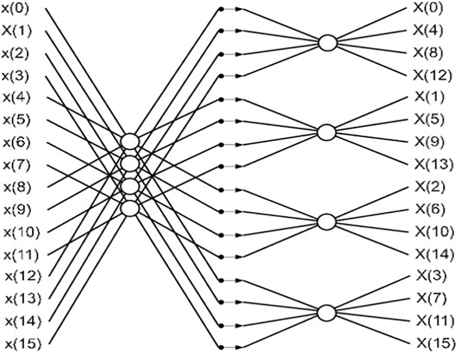
Figure 1: Radix-4 16-point FFT BF structure
Fig. 2 shows the structure of the FWFT BF for 16-point radix-4. There is a low amount of real-time addition in radix-4 FWFT and multiplication is required. Four points are added to each stage and the values are calculated to be sent to the next stage of the BF. In addition, one more expansion may be reduced by the use of the butterfly structure and 3 multiplication and 15 additions are used for each butterfly.
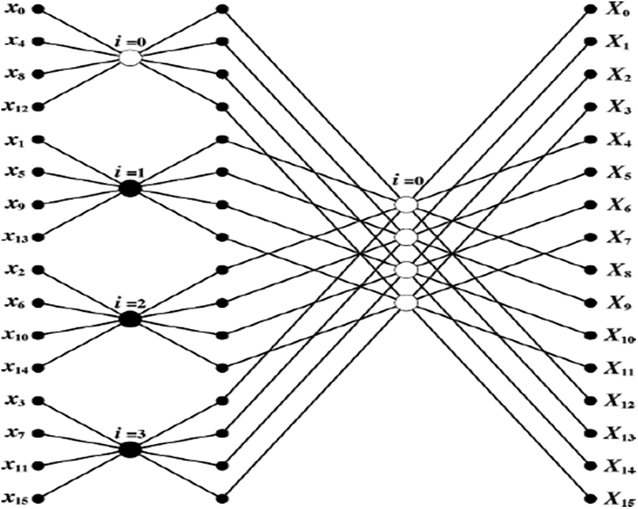
Figure 2: FWFT 16-point radix-4 BF structure
In the proposed method, a novel FWFT algorithm is used to achieve a very low complexity of the NOMA system and most importantly, the time requirement for the proposed methodology is very low with the help of the logic circuit. After determining the FWFT value, this system is implemented in the VLSI architecture to make the NOMA system a real-time purpose.
Block diagram of pass logic circuit based FWFT shown in Fig. 3, it consists of a small amount of addition and multiplication in real time. The adder for real-numbers is compatible with the subtractor. Real and imaginary components interweave the input/output data. In FWFT there are many multipliers are presented at the input side to multiply real and imaginary part of the butterfly values. The multipliers in the input stage Radix-4 butterflies accept one input, m as somewhat of {–1, 0, +1). Those values are replaced into PL which takes m as any one of {11,00,01,10}. Here the pass logic played an important role because it replaced the multipliers with a single circuit so, the transistor required for those methods will better. The area and power need for this technique are very low. Pass logic frequently customs less transistors, scores faster, and wants less power than CMOS logic. The first stage data processing order for the 16-point FWFT system for NOMA transmission is discussed below,
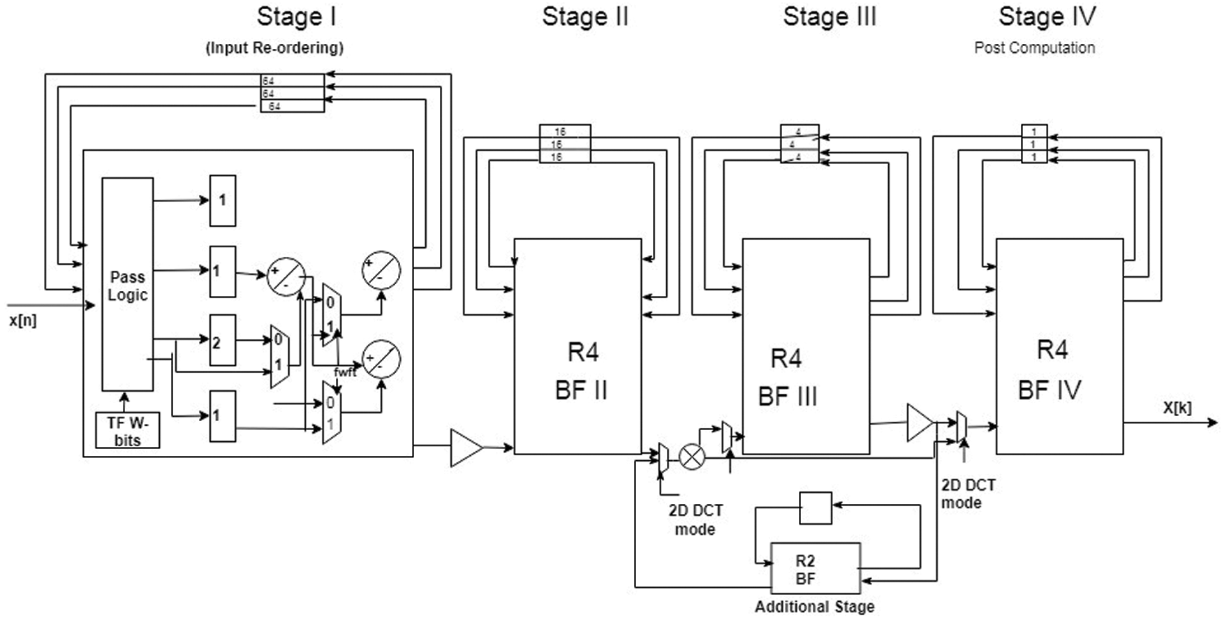
Figure 3: Block diagram of pass logic circuit based FWFT
3.1 A Novel FWFT Method for NOMA Transmission
In order to minimize the latency in hardware implementation, this study offers an effective method with parallel approach that dramatically limited the size of iterations. Meanwhile, it performs admirably. Fig. 4 shows the complex performance of radix-4 FWFT computation. For example, one radix-4 butterfly may take up the role of up to four other radix-2 butterflies, and it only includes three complex multipliers as contrasted to the four complex multipliers required by four radix-2 butterflies. In optimal controlled, there is a low amount of real-time addition and multiplication is required in radix-4 FWFT. Optimization in FFT for speed improvement has done via the proposed radix-4 FWFT structure normally radix-2 for the higher bit length induces latency. The architecture consists of four real-number adders and two real-number multipliers, one commutator, four multiplexers, and some other components, as shown in Fig. 3. The adder for real numbers is compatible with the subtractor, real and imaginary interleave the input/output data as a result of the distance between two operators of the buffer size is described by
Figure 4: Radix 4 FWFT computation
Basically, an FWFT is a transform technique which is used to a pair of DFT and WHT. When compared FWFT with FFT, this method reduces complexity by log2(N)-1 and it uses FWFT to evaluate the pair of DFT and WHT. The modulated signal vector is signified as
Then Q is retrieved from the forward FWFT process which is expressed as,
where
The column bit inverse direction changes G and H’s underlying S point DFT matrix.
If IFWFT is utilized on the transmission side, the IFWFT matrices N and S can be expressed in terms.
We can see that M[N] is a piece transversal matrix, with two-thirds of its components having zero.
Assume G [
In M [16], the sub-matrix
where X [4] and Y [4] can be correspondingly written as
Define w =
Then,
As well,
Fig. 6 shows the pass logic function in which the multiplication is performed with the help of the pass logic circuit. From this figure, we can clearly say that the upper part of the circuit only has an additional part, while the lower part has a multiplication with a smaller number of transistors. M Prakash et al suggested a PL circuit to decrease the number of transistors needed for operation, where the PL butterfly diagram is shown in Fig. 5. So, it consumes very little power. The result shows that the transistor controls the delay and the control transmitter for the specific power.
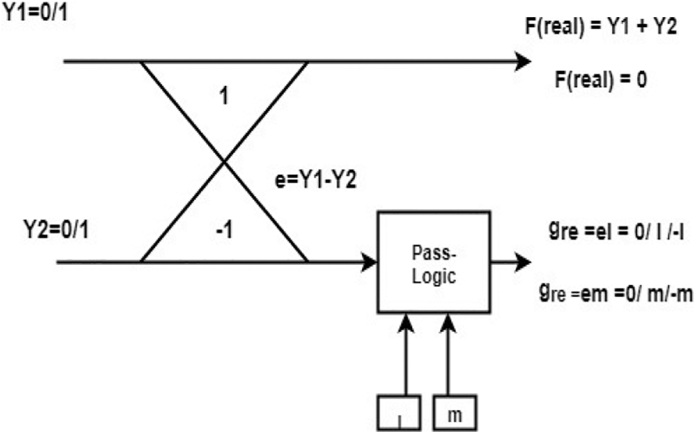
Figure 5: PL butterfly diagram to decrease the number of multipliers
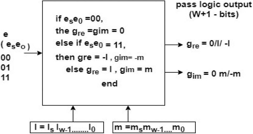
Figure 6: Pass logic circuit
The normal multiplier requires more adders and shift operators to perform this function. But this is going to create the worst stage when the number of operations increases. However, in this proposed method, the 16-point radix-4 FWFT method uses PL circuits instead of multiple multipliers. As a result, requirements for hardware and capacity are significantly minimized. The range of complexity is condensed. Despite this, there is no variation in the time of implementation in the different input values.
When more multipliers are used, the number of gates increases, but the gate range decreases with the help of pass logic.
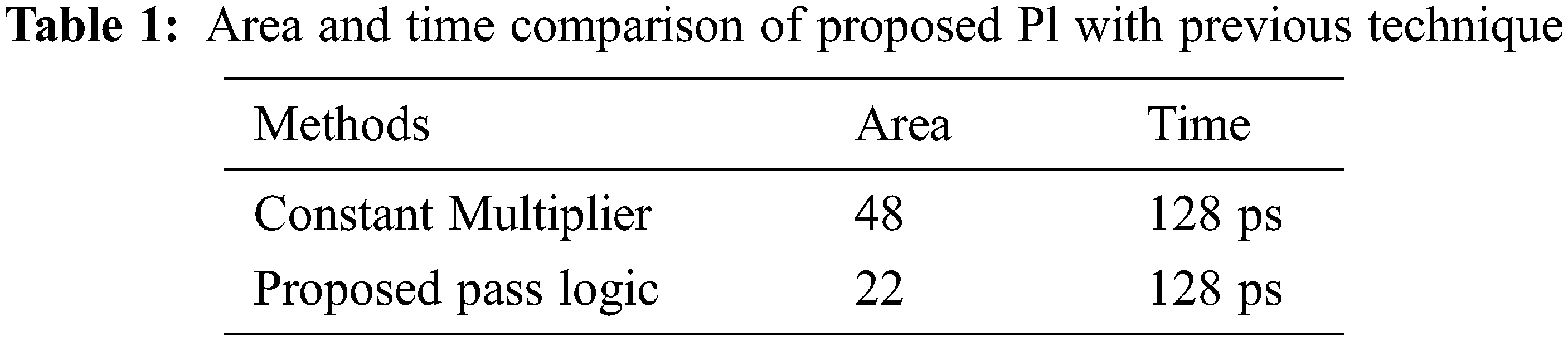
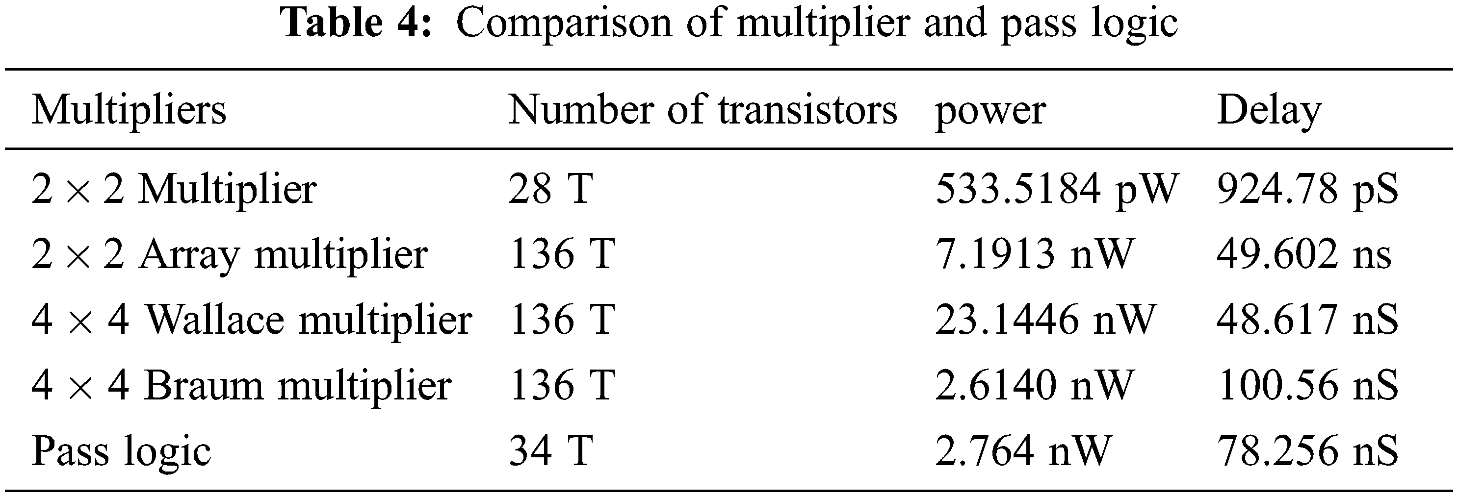
The Tab. 1 shows the comparison of constant multiplier and proposed PL, based on the values present in the table, we can say that the number of gates required for the constant multiplier is 48 and for PL, the required gate number is 22. If the number of gates decreased, then the size will also decrease. This has a great impact on many applications related to logic gates. But one major thing behind this concept is, it required the same time as constant multiplier need.
3.3 Additional 2D DCT for BF Structure
The 2-D DCT is implemented directly from the theoretical equation, which yields 1024 multiplications and 896 additions. Fast algorithms take advantage of the DCT’s symmetry to achieve significant computational savings. The discrete Fourier transform is related to the DCT in that it converts a signal from the time domain to the frequency domain. It lowers the number of memory and bandwidth needed for digital signals dramatically. The 2-D DCT stands for two-dimensional Discrete Cosine Transform which is applicable to calculate the transform function. The common DCT equation is given as,
The adder’s outputs are saved in RAMs. When the WR signal is large, the write operation is performed on the corresponding RAM address. Otherwise, the RAM address’s contents are read. The address signals have a length of 64 times the input clocks. Two ROMs are used to allow for continuous data writing. The outputs of the eight multipliers are then added together to produce 1D coefficient values that are saved in RAM. The intermediate RAM values are read out one column at a time (every 8th value is read out every clock), and this is the input for the 2nd DCT. The
3.3.1 The Extra Period of 2-D DCT
3.3.2 The Time-domain Shift Period of 2-D DCT
The 2-D DCT calculation occurs and X-2 [8k-1+k-2] is determined simultaneously within the B arrangement IV post-calculation. The mathematical 8 x 8 2-D IDCT has been clarified using the process of deterioration. This reflects the triple-mode FFT/ IFFT and 2-D DCT equation to be tested as a consequence of the cost-effective imperative within the physical plan. Determination returns on the FFT/IFFT/2-D DCT calculation based on Radix-4^2 shows that BF calculation could be effectively performed in four complicated input adders and a few trail circuits. No multipliers are used in the Radix-4 BF structure. In addition, the pair of 8 x 8 2-D DCT and 256-point FFT/IFFT pipeline procedure designs can be calculated by a standard structure. DCT is implemented using a framework called vector processing with parallel multipliers. Regular structure, easy control and interconnect, and a reasonable compromise between efficiency and complexity of implementation are all advantages of vector processing.
4 Hardware & FPGA Implementations
The described NOMA FPGA organization is executed on the USRP-RIO 2953R National Instruments SDR platform. The key benefit of this stage is the integrated Kintex7-FPGA, which enables the hosting of all the related portions of the signal processing. The RF channels is another major benefit that provides several tools for design synthetization, formation methods, and concert investigates, including resource, speed, and power consumption. This makes a single device NOMA transceiver without the need for synchronization and data transmission with only one channel between multiple front-ends. The USRP-RIO has a frequency range of 1.2 to 6 GHz, a bandwidth of 40 MHz, and a throughput rate of 832 MB/s. The USRP is linked to a PC using the NI PXIe-PCIe8371 card. The USRP-2953 is a complete equipment / software package for quickly developing high-performance wireless communications networks. The USRP typically enables progressive waveforms to be conveniently prototyped in an occurrence series that encompasses the key bandwidths used today for portable transportations. One more major advantage of this stage is that it is possible to moderately implement the communication chain in hardware and software. Project Set is a versatile way of exploring the flexibility of SDR shared with the execution of FPGA by integrating software roles in a block group considered with a hardware description language. Researchers can design better and also get results faster with USRP RIO’s combined hardware and software package. Multiple input, multiple output (MIMO); synchronization of wireless links; LTE relay; RF compression filtering; spectral sensing; cognitive radio; frequency hopping; and orientation mapping are among the important research technologies they can develop. The design process of FPGA is given in Fig. 7. After the FPGA employment, the total power and time were calculated using a power analyzer and timing analyzer based on that the consumed power and time. It is also an important part of the iterative process of optimizing FPGA performance. It can help improve/optimize timing performance and consistency. Finally, the complexity range of FWFT is compared with respect to a number of stages.
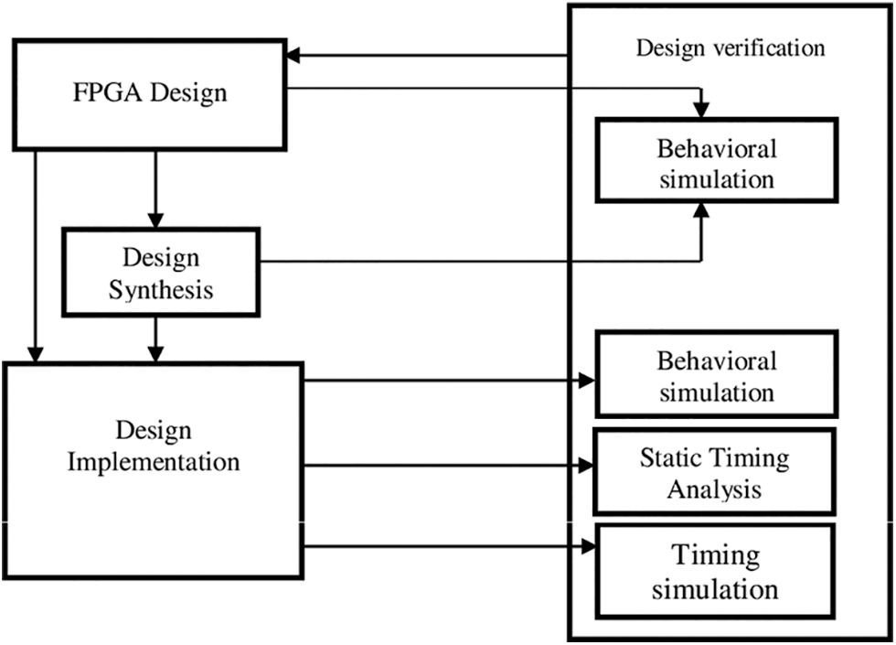
Figure 7: Design flow of FPGA
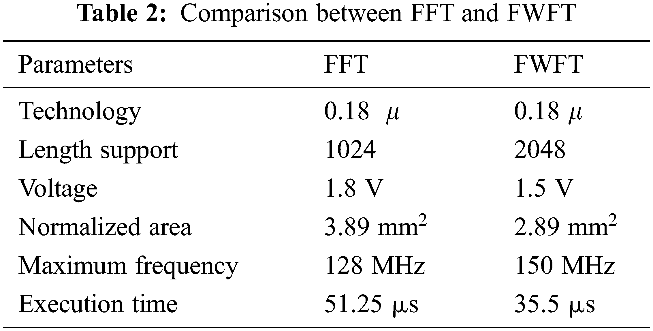
Tab. 2 explains the comparison between FFT and FWFT. When compared with FFT, FWFT has a greater advanced related to time, area and frequency. In other previous methods, there is no pass logic and FPGA implementation were presented for the FWFT technique. Hence, this paper presents the VLSI implementation for FWFT to improve the NOMA system performance with respect to complexity and power requirement. Based on this research the complexity is reduced with the help of pass logic circuit. In previous papers, the number of transistors required for multiplication was very high and which required more power to run and designing complexity was also high. In order to avoid this problem, a novel pass logic circuit attached to FWFT is implemented.
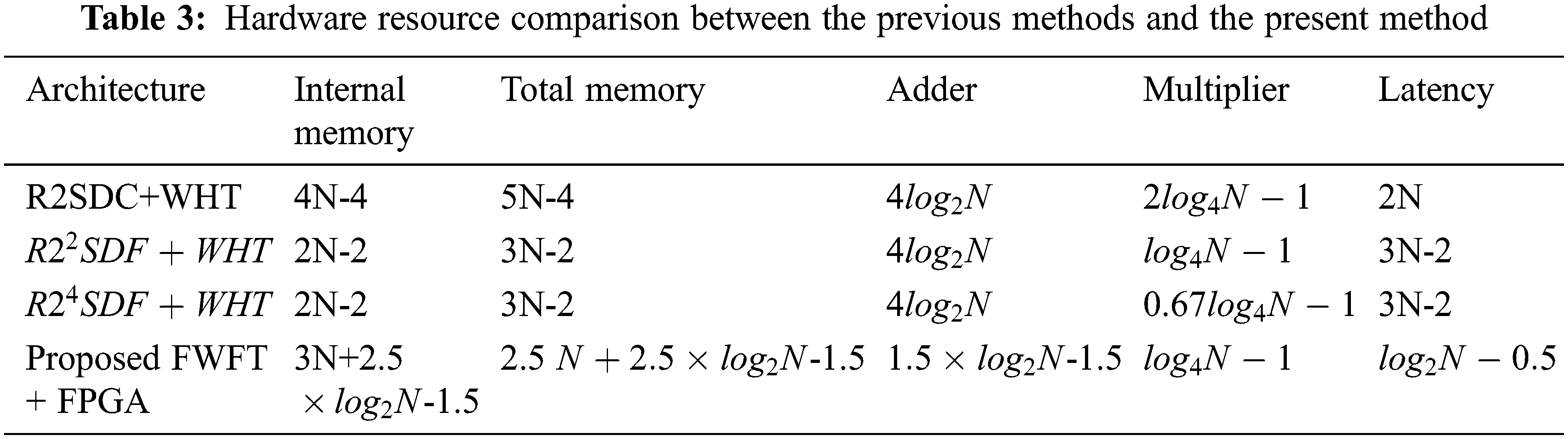
Tab. 3 compares some parameters for previous methods and present FWFT+FPGA method. The parameters which include internal memory, overall memory, adder, multiplier, and latency. When compared the values, we can say that, this FWFT method is better compared with other methods and the comparison of multiplier and pass logics are shown in Tab. 4
Complexity analysis: For the transmission and receipt of a given number of multi-carrier symbols, the complexity analysis of each contender is assessed as the required number of complex multiplications. Fig. 8 shows the number of complex multiplications in relation to the number of blocks. The FWFT operation is known to require a complex multiplication of
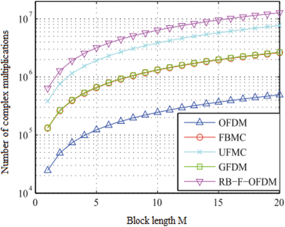
Figure 8: Block length vs. number of complex multiplications
However, compared to the existing techniques, the proposed FWFT-NOMA-FPGA techniques reduce the number of complex multiplications with the help of the pass logic circuit. FBMC and GFDM are the most effective waveforms and are five times more complex than OFDM. RB-F-OFDM and UFMC are more complex as each sub-band generates FWFT operations and is 10 times more complex than the modulated OFDM data symbol.
A comparison of the computational complexity of the various waveform schemes is shown in Fig. 9. The complexity is quantified by the total number of actual multiplications per symbol. For the transmitter and receiver, the effect of the number of subcarriers on the complexity of waveforms has been measured and compared.
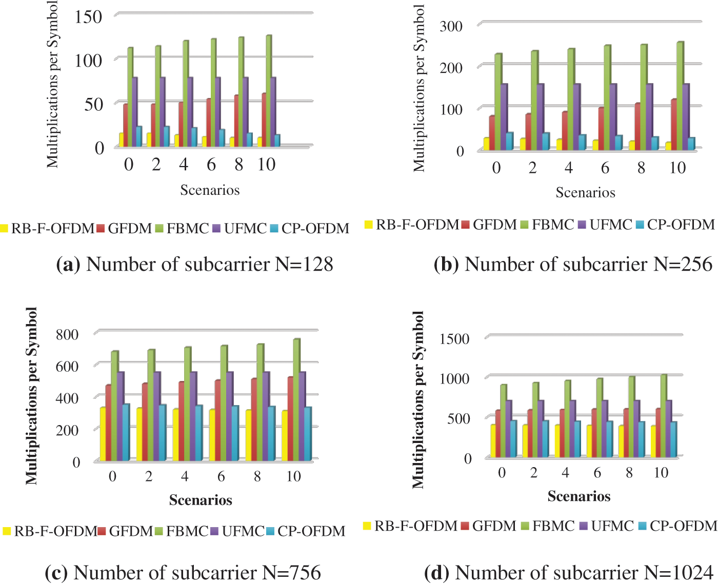
Figure 9: Comparison of computational complexity for the various waveform schemes (a) N = 128 (b) N = 256 (c) N = 756 (d) N = 1024
Compared to existing techniques, GFDM has less than three times the number of operations, while FBMC has seven times the number of operations, and UFMC has more than nine times the number of operations. As predicted, although the simplest waveform is CP-OFDM, the more complex waveform (FBMC) shows only substantial complexity differences for N = 756 subcarriers is shown in Fig. 9c. CP-OFDM and RB-F-OFDM are two times less complex than FBMC and 1.5 times less complex than GFDM and UFMC for N = 1024 subcarriers are present is shown in Fig. 9d. For
This paper presents the FPGA implementation of FWFT to make the FWFT algorithm fast and real time. With the help of FPGA and Pass logic, the proposed architecture achieves more hardware utilization and low complexity. When the FPGA was implemented, the number of transistors decreased by 21% and the total power required was reduced by 5.5%. The FPGA implementation of FWFT for 34 transistor-pass-logic customs and power consumption is 2.764 mW with a latency of 78.256 ns. As a result, the proposed system has achieved a less power, less area and low complexity system that can improve the operation of the MIMO system. Most importantly, the time requirement for the proposed methodology is very low so that it could become a promising model for the MIMO system for future 5G technology.
Acknowledgement: The authors would like to thank Anna University and also, we like to thank Anonymous reviewers for their so-called insights
Funding Statement: The authors received no specific funding for this study.
Conflicts of Interest: The authors declare that they have no conflicts of interest to report regarding the present study.
1. L. Lv, J. Chen, Q. Ni, Z. Ding and H. Jiang, “Cognitive non-orthogonal multiple access with cooperative relaying: A new wireless frontier for 5G spectrum sharing,” IEEE Communications Magazine, vol. 56, no. 4, pp. 188–195, 2018. [Google Scholar]
2. A. Anbarasan and K. Shankar, “Design and implementation of low power FFT/IFFT processor for wireless communication,” in Proc. PRIME, Salem, India, pp. 152–155, 2012. [Google Scholar]
3. L. Luo, Q. Li and J. Cheng, “Performance analysis of overlay cognitive NOMA systems with imperfect successive interference cancellation,” IEEE Transactions on Communications, vol. 68, no. 8, pp. 4709–4722, 2020. [Google Scholar]
4. B. T. Wang and J. B. Kuo, “A novel low-voltage silicon-on-insulator (SOI) CMOS complementary pass-transistor logic (CPL) circuit using asymmetrical dynamic threshold pass-transistor (ADTPT) technique,” in Proc. IEEE, Circuits and Systems, Lansing, MI, USA, pp. 694–697, 2000. [Google Scholar]
5. C. Kang, Y. Liu, H. Meixia and H. Zhang, “A low complexity PAPR reduction method based on FWFT and PEC for OFDM systems,” IEEE Transactions on Broadcasting, vol. 63, no. 2, pp. 416–425, 2017. [Google Scholar]
6. C. T. Lin, C. Y. Yuan and L. D. Van, “Cost-effective triple-mode reconfigurable pipeline FFT/IFFT/2-D DCT processor,” IEEE Transactions on Very Large-Scale Integration (VLSI) Systems, vol. 16, no. 8, pp. 1058–1071, 2008. [Google Scholar]
7. D. F. G. Coelho, R. J. Cintra, N. Rajapaksha G. J. Mendis,A. Madanayake and V. S. Dimitrov, “DFT computation using gauss-eisenstein basis: FFT algorithms and VLSI architectures,” IEEE Transactions on Computers, vol. 66, no. 8, pp. 1442–1448, 2017. [Google Scholar]
8. H. Xiao, X. Yin, N. Wu, X. Chen, J. Li et al., “VLSI design of low-cost and high-precision fixed-point reconfigurable FFT processors,” IET Computers and Digital Computers, vol. 12, no. 3, pp. 106–110, 2018. [Google Scholar]
9. J. Liu, X. Qianjian, Y. Xiaobo, X. Mao and Y. Feng, “Pipelined architecture for aradix-2 fast walsh-hadamard-fourier transform algorithm,” IEEE Transactions on Circuits and Systems ll: Express Briefs, vol. 62, no. 11, pp. 1–5, 2015. [Google Scholar]
10. N. Mahdavi, R. Teymourzadeh and M. B. Othman, “VLSI implementation of high speed and high resolution FFT algorithm based on radix 2 for DSP application,” in Proc. RD, Selangor, Malaysia, pp. 1–4, 2007. [Google Scholar]
11. M. Garrido, M. A. Sanchez, M. L. V. Lopez and J. Grajal, “A 4096- point radix-4 memory- based FFT using DSP slices,” IEEE Transactions on Very Large-Scale Integration (VLSI) Systems, vol. 25, no. 2, pp. 375–379, 2018. [Google Scholar]
12. A. Marwan, Jaber and D. Massicotte, “A new FFT concept for efficient VLSI implementation: Part I - butterfly processing element,” in Proc. DSP, Santorini, Greece, pp. 1–6, 2009. [Google Scholar]
13. M. T. Hamood and S. Boussakta, “Fast walsh-hadamard–fourier transform algorithm,” IEEE Transactions on Signal Processing, vol. 59, no. 11, pp. 5627–5631, 2011. [Google Scholar]
14. G. Prathiba, M. Santhi and A. Ahilan, “Design and implementation of reliable flash ADC for microwave applications,” Microelectronics Reliability, vol. 88, no. 90, pp. 91–97, 2018. [Google Scholar]
15. A. Remon, E. S. O. Quintana and G. Q. Orti, “Solution of band linear systems in model reduction for VSLI circuits,” Scientific Computing in Electrical Engineering, Springer, vol. 11, pp. 387–393, 2007. [Google Scholar]
16. R. T. Gonzalez, P. Reviriego, J. A. Maestro and Z. Gao, “Scheme to design concurrent error detection techniques for the fast fourier transform implemented in SRAM-based FPGAs,” IEEE Transactions on Computers, vol. 67, no. 7, pp. 1039–1045, 2017. [Google Scholar]
17. S. Teng and Y. Feng, “A family of fast hadamard-fourier transform algorithms,” IEEE Signal Processing Letters, vol. 19, no. 9, pp. 583–586, 2012. [Google Scholar]
18. X. Y. Shih, H. R. Chou and Y. Q. Liu, “VLSI design and implementation of reconfigurable 46-mode combined-radix-based FFT hardware architecture for 3GPP-LTE applications,” IEEE Transactions on Circuits and Systems, vol. 65, no. 1, pp. 118–129, 2018. [Google Scholar]
19. K. Yano, T. Yamanaka, T. Nishida, M. Saito, K. Shimohigashi et al., “A3.8-ns CMOS 16 x 16-b multiplier using complementary pass-transistor logic,” IEEE Journal of Solid-State Circuits, vol. 25, no. 2, pp. 388–395, 1990. [Google Scholar]
20. C. Ajitha and T. Jaya, “Cognitive radio technology with reduced PAPR and complexity for IoT-based OFDM networks,” Peer-to-Peer Networking and Applications, vol. 13, no. 6, pp. 2065–2077, 2020. [Google Scholar]
 | This work is licensed under a Creative Commons Attribution 4.0 International License, which permits unrestricted use, distribution, and reproduction in any medium, provided the original work is properly cited. |