DOI:10.32604/iasc.2023.025866
| Intelligent Automation & Soft Computing DOI:10.32604/iasc.2023.025866 | |
| Article |
Buck Converter Current Measurement Using Differential Amplifier
Department of Electrical and Electronics Engineering, Coimbatore Institute of Technology, Coimbatore, 641014, India
*Corresponding Author: P. Rajeswari. Email: rajeswaripphd@gmail.com
Received: 07 December 2021; Accepted: 18 January 2022
Abstract: The accuracy of the measured current is a preeminent parameter for Current Control based Power Converter applications to ensure genuine operation of the designed converter. The current measurement accuracy can be affected by several parameters which includes the type of technology used, components used for the selected technology, aging, usage, operating and environmental conditions. The effect of gain resistors and their manufacturing tolerances on differential amplifier-based buck converter current measurement is investigated in this work. The analysis mainly focused on the output voltage variation and its accuracy with respect to the change in gain resistance tolerances. The gain resistors with 5%, 1%, 0.5% and 0.1% manufacturing tolerances taken for the worst-case analysis and the calculated performance results are compared and verified with the simulation results. The Operational amplifiers (Op-Amp) for high frequency power converter applications must operate in a high frequency noise environment and the intended current measuring system must manage common mode noise disturbances paired with the signal to be measured. Based on the Common Mode Rejection Ratio (CMRR) the common mode voltages and noise signals will effectively get filtered out. Lesser CMRR results in lower common mode signal rejection, resulting in poor precision and noise rejection. In differential amplifiers, the CMRR predominantly depends on gain resistors. So, the variations in Common Mode Rejection Ratio due to gain resistor tolerances also analyzed and compared with the output voltage variations. Besides the effects of resistor tolerances, this paper also examines the effect of Op-Amp offset voltage on output accuracy specifically for low magnitude input currents. The obtained results from this analysis clearly shows that the gain resistors with 0.1% tolerance gives maximum accuracy with improved CMRR and accuracy at low magnitude input currents will get well improved by using Op-Amps with Low Offset voltage specifications.
Keywords: Buck converter; common mode rejection ratio; common mode gain; current sensing; differential amplifier; differential mode gain; shunt resistor
In modern electronics designs, the power converters designed with current mode control [1,2] becoming most promising solution due to its excellent performance characteristics which ensures the efficient and stable operation at different operating conditions. The acquisition and accuracy of input current signals which are given to the compensation system is a basic and mandatory parameter in order to deliver the better control as per system requirements. There are different types of technologies are available to measure the current [3,4] and a suitable technology can be selected based on the isolation, power dissipation, measurement current level, system size, component count and costing requirements. Along with those requirements and considerations the system accuracy will be final product of any measurement techniques and extreme efforts are made to reach the maximum accuracy and minimum error.
Based on the method of measurement, the Current sensing technology can be divided in two major groups of Resistance Current Sensing and Magnetic Current sensing. In traditional resistive direct Current sensing, the current is converted into voltage directly by using Ohms law. In Power Converter applications the external low resistance shunts, Current Sensing Power MOSFETs (SENSEFETs) [5], Metal Oxide Semiconductor Field Effect Transistor (MOSFET) Rds_on [6], Inductor Direct Current Resistance (DCR) [7,8] and Printed Circuit Board track resistances [9] are used to convert the series flow current into equivalent voltage and fed into the microcontroller or analog control circuitry. The magnetic indirect current sensing measures current by converting it into the magnetic field and the converted magnetic field is measured in terms of voltage. The magnetic current sensing technology commonly implemented through Current transformer [10–12] and Hall based current sensors technology [13–15].
In both resistive and magnetic based current measurement techniques, the obtained equivalent output voltage is low and contains high frequency noises. Before fed into the microcontroller or analog control circuits, the obtained output voltages is fed to signal conditioning circuit to increase the voltage to the required level and to remove the overlaid undesirable noises in the measurement signal. The Op-Amp based signal processing is used in most of the circuits due to its attractive cost and size advantages. Among different Op-Amp based solutions, the differential Op-Amp based current measurement system widely used in high side, bidirectional resistance based current measurement and Hall Sensor based current measurement systems.
For any Op-amp based signal conditioning circuits the important design parameters are accuracy of output voltage and better common mode noise rejection. In differential amplifier based measurement systems the gain resistors are the most important parameters in defining accuracy of the output response. In this work, the differential op-amp output voltage accuracy issues due to the op-amp gain resistance tolerances in the buck converter current measurement circuit are taken for the analysis. The gain resistor effects in CMRR also taken for analysis in order to compare the effect of common mode gain in deciding final measurement accuracy. The buck converter which current to be measured have the below specifications Vin = 20 to 26 V, Vout = 12 V, Iout = 10 A, VCurrent_10A = 2.5 V. The maximum measurement current requirement is 10A and the Shunt based current measurement is preferred with maximum allowed power loss in shunt resistor is 1% of maximum output power. So, PShunt_Max = 1.2 W. To match the power dissipation requirements the 10 mΩ shunt resistance is selected. The maximum obtained voltage in the shunt resistor for 10A current is 100 mV and to match the requirement of 2.5 V at 10A input current the differential amplifier circuit is used to convert the low shunt voltage into required 2.5 V Level.
2 Implementation of Differential Amplifier for High Side Current Measurement
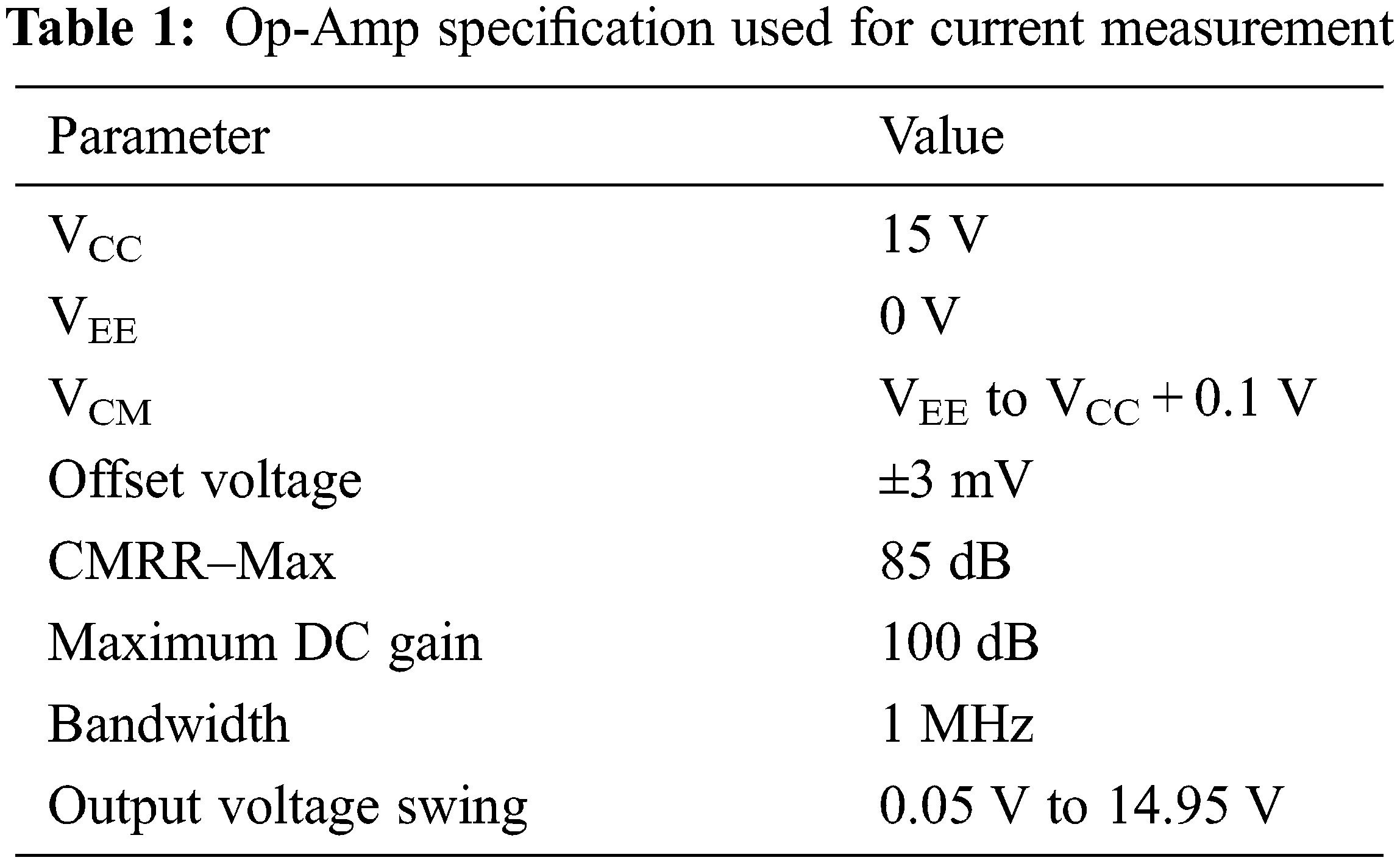
The implementation of differential amplifier based High side buck converter current measurement is shown in Fig. 1. The specifications of the LM324 equivalent Op-Amp used for the current measurement analysis are given in Tab. 1. The buck converter taken for this analysis is designed for constant 12 V output and 10 mΩ Shunt resistance is used to measure the Current. The target output voltage of the differential op-amp at 10 A is 2.5 V and at 0 A is 0 V. So, the required gain value of the differential op-amp is 25 V/V. In order to obtain the gain, the selected gain resistance values are RA = RB = 20000 Ω and RC = RD = 800 Ω.
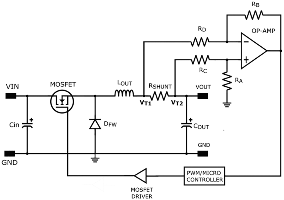
Figure 1: Differential Op-Amp based buck converter current measurement circuit
Due to the manufacturing variations and various operating conditions the resistors have tolerances and the resistance values may get increased or decreased based on the tolerance values and operating conditions. The output voltage relation of the differential amplifier for the nominal gain resistance values is given in Eq. (1)
where,
Vout–Differential Op-Amp Output Voltage
VT1–Voltage at Shunt Resistor terminal 1
VT2–Voltage at Shunt Resistor terminal 2
RA, RB, RC, RD–Differential Op-Amp Gain Resistors
The Shunt terminal voltages VT1 and VT2 with respect to Common Mode Voltage and differential voltage across Op-amp terminals given in Eqs. (2) and (3)
where,
Vcm–Common Mode Voltage
Vdm–Differential Mode Voltage
Substituting Eqs. (2) and (3) in (1) the final simplified equation is
Acm–Common Mode Gain
Adm–Differential Mode Gain
The Common Mode Gain (Acm) and the Differential Gain (Adm) is given in Eqs. (5) and (6) respectively.
In practical conditions due to the gain resistors tolerance values (
where,
Meanwhile, the worst-case minimum value of differential mode gain is given in Eq. (8)
Likewise, the worst case maximum common mode gain with respect to maximum differential gain can be obtained using Eq. (9)
The Eq. (10) is used to calculate the minimum common mode gain value with respect to the minimum differential gain condition.
Based on the above equations the gain resistors with the tolerance values (
Also in order to verify the calculation results and to analyze the variation in output voltage due to Op-Amp output rail limitation and input offset voltage the worst case simulation has performed for Op-amp Offset voltage of ±3 mV and Op-amp maximum output voltage is limited to 14.95 V and minimum output voltage is 0.05 V. The calculated and simulated response of differential op-amp output for all gain resistors with 5% tolerance is given in Fig. 2.
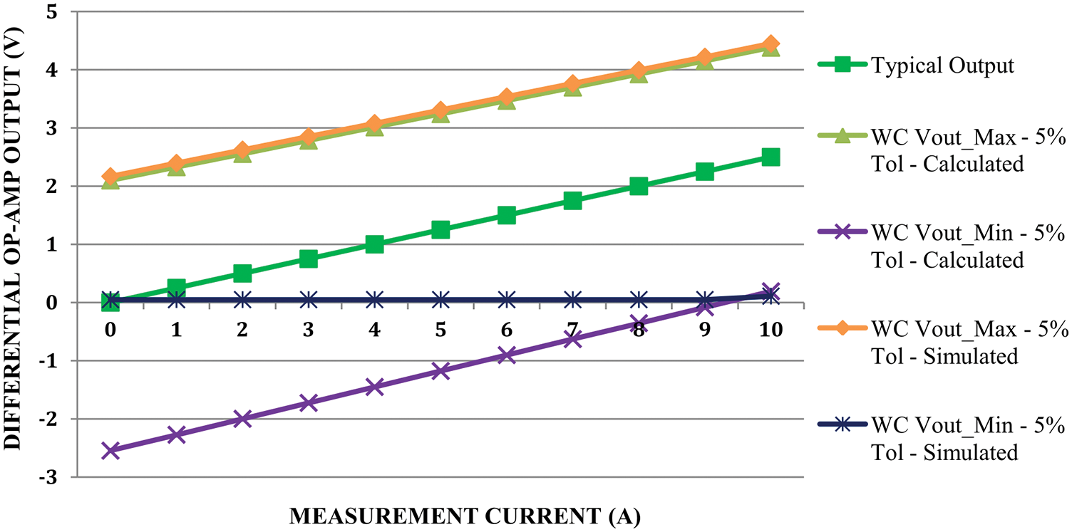
Figure 2: Worst case differential Op-Amp output for gain resistors with 5% tolerance
With 5% resistance tolerance the deviation between typical output voltage and the worst-case maximum and minimum output voltage is too high. For Lower magnitude input current conditions, as per the calculated results the output voltage (WC Vout_Min–5% Tol Calculated) reaches negative voltage region whereas in simulation due to Op-Amp low rail saturation voltage the simulated output voltage (WC Vout_Min–5% Tol Simulated) is limited to 50 mV and the equivalent measured current nearly zero for entire range. Meanwhile for worst case maximum output conditions the Op-Amp output voltage reaches 2 V for zero current input which is the respective output voltage for 8A input current in nominal operating conditions.
The differential op-amp output voltage with 1% tolerance values are given in Fig. 3. Compared to 5% resistance tolerance for 1% tolerance gain resistors the difference between typical value and worst-case maximum and minimum values is low and the overall accuracy well improved.
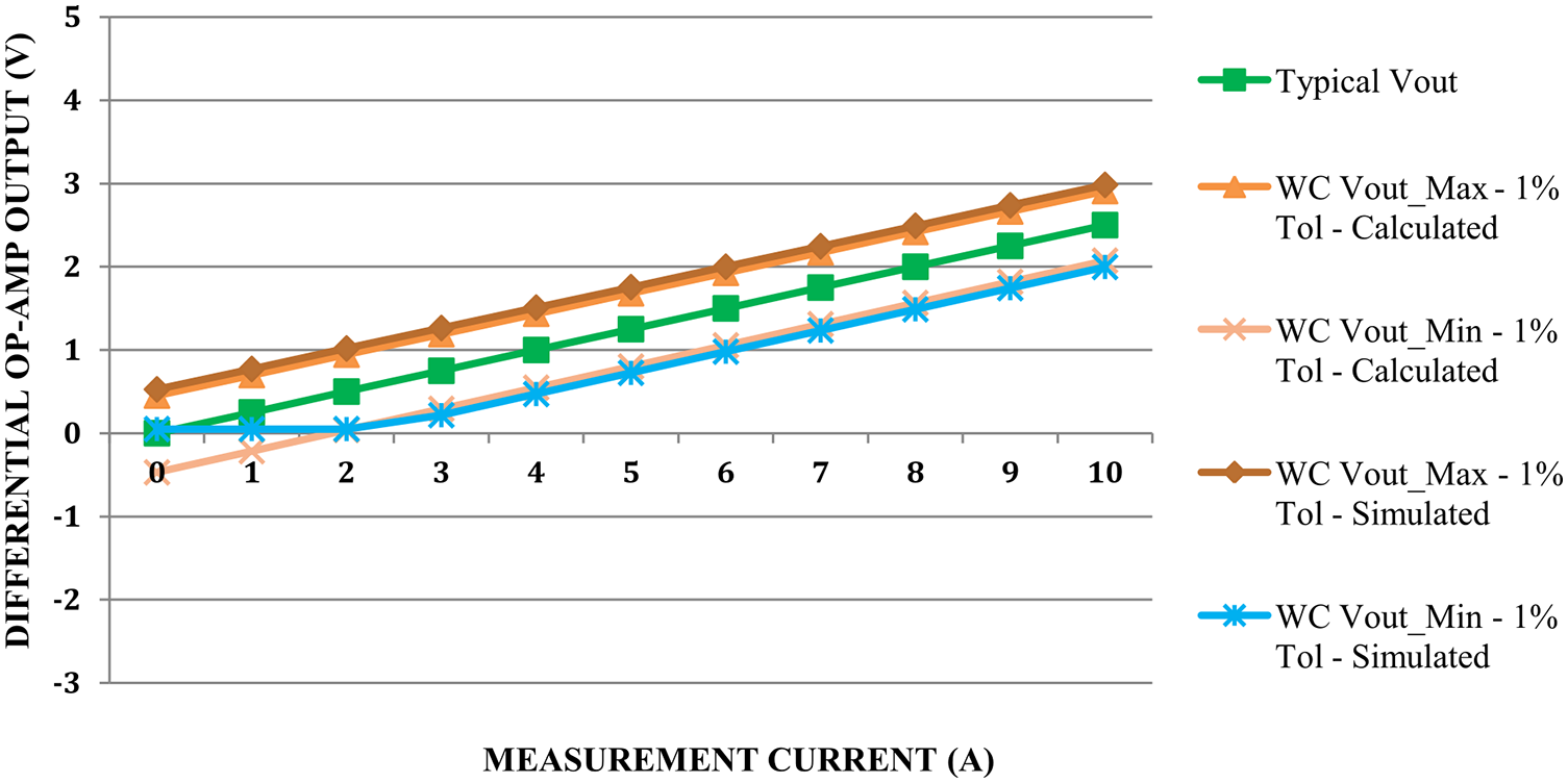
Figure 3: Worst case differential Op-Amp output for gain resistors with 1% tolerance
The maximum and minimum error percentage comparison for differential op-amp current measurement with 5% and 1% resistance tolerances are shown in Figs. 4 and 5 respectively. With 5% tolerance condition the positive error is varied between 859% and 78% based on the input current, whereas the negative tolerance is varied between −96% to −80% due to output voltage reaches Op-Amp negative rail saturation. With 1% tolerance the accuracy is improved compared to the 5% case where the positive error is varied between 209% and 19%. The negative error for 1% tolerance lies between −80% and −20%. However, in low input current conditions still the error percentage is higher with 1% tolerance resistors.
Figure 4: Worst case maximum error percentage for gain resistors with 5% and 1% tolerance
Figure 5: Worst case minimum error percentage for gain resistors with 5% and 1% tolerance
The output voltage response with 0.5% gain resistance tolerance is given in Fig. 6. The difference between nominal voltage range and worst-case voltage ranges with 0.5% tolerance is less than the prior case. In worst case calculation the worst-case minimum voltage under low input current conditions is less than op-amp low rail voltage and in simulation those low current responses maintained in 50 mV range.
Figure 6: Worst case differential op-amp output for gain resistors with 0.5% tolerance
The output voltage response with 0.1% gain resistance tolerance is given in Fig. 7 and the voltage deviation is comparatively less than all prior cases with 0.1% tolerance and the error current is around 500 mA.
Figure 7: Worst case differential op-amp output for gain resistors with 0.1% tolerance
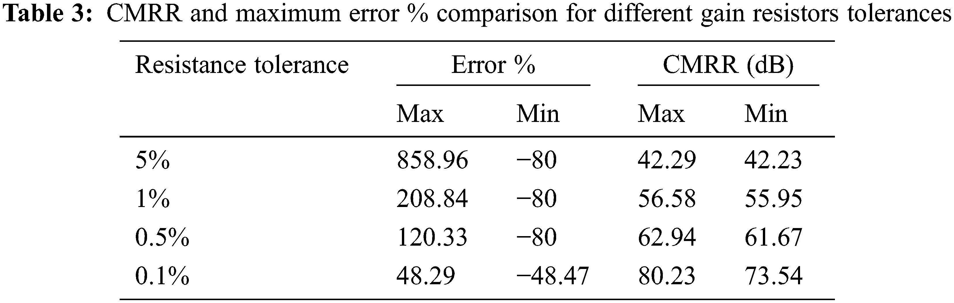
The maximum and minimum Error percentage with 0.5% and 0.1% resistance tolerance is shown in Figs. 8 and 9. Based on Figs. 8 and 9 data the maximum error percentage with 0.5% gain resistance tolerance the positive error is varied between 120% to 11.3% based on input current and negative error values lies among −80% to −11.52%. In 0.1% tolerance condition the positive tolerance is under low input current greatly reduced and the percentage of error varies between 48.3% and 4.75%. The maximum value of negative error with 0.1% tolerance is −48.47% and minimum value negative error is −4.77%.
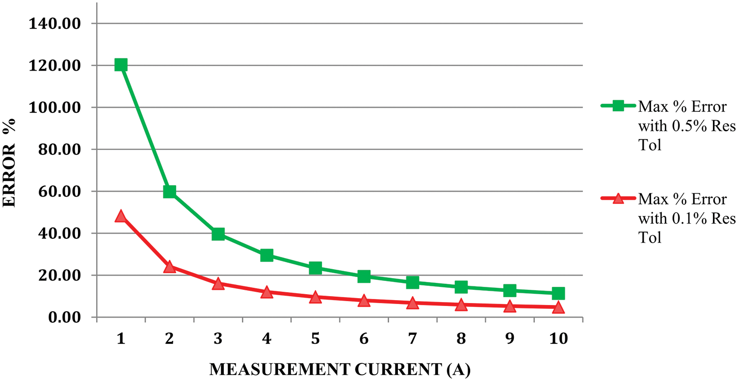
Figure 8: Worst case maximum error percentage for gain resistors with 0.5% and 0.1% tolerances
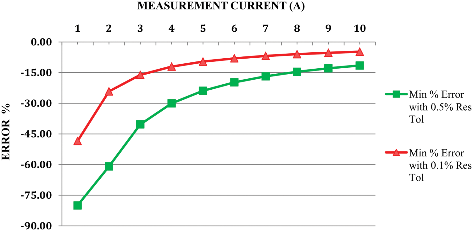
Figure 9: Worst case minimum error percentage for gain resistors with 0.5% and 0.1% tolerances
By comparing the Fig. 8 with Fig. 4 the worst case maximum error percentage is reduced from 859% to 120% for minimum input current condition whereas for maximum current condition it is reduced to 4.75% from 78% and the same condition also resembles in negative error percentage irrespective of clamping due Op-Amp low rail saturation limits.
3 Analysis of Effects in Common Mode Rejection Ratio Due to Gain Resistance Tolerances
The Common Mode Rejection Ratio (CMRR) [16,17] is a significant parameter for Op-Amp circuits which shows the ability of an Op-amp on Common mode signal or common mode noise rejection. The Op-Amps used for Buck converter current measurement are designed to measure DC currents with high frequency ripples and high frequency pulse currents.
Due to the parasitic elements present in switching devices, inductors and printed circuits boards the high frequency common mode noise signals such as common mode voltage due to ground shifting, noises due to high frequency voltage and current transients, noises induced from nearby or external circuitry are coupled with op-amp input signals and proper rejections of those common mode signal noises is a mandatory requirement in order to ensure the precise and noise less output voltage.
Apart from Op-amp internal parameters defined by Op-amp manufacturers, the variations in gain resistance values due to its tolerances are the dominant factors in deciding Common Mode Rejection Ratio. The CMRR response of the differential amplifier with ideal resistance values RA = RB = 20000, RC = RD = 800 is given in Fig. 10. The CMRR of the differential op-amp with ideal resistance values is 84.96 dB and the Common Mode gain is −57 dB. The CMRR response of Op-Amp under maximum differential gain condition with 5% resistance tolerance is given in Fig. 11a.
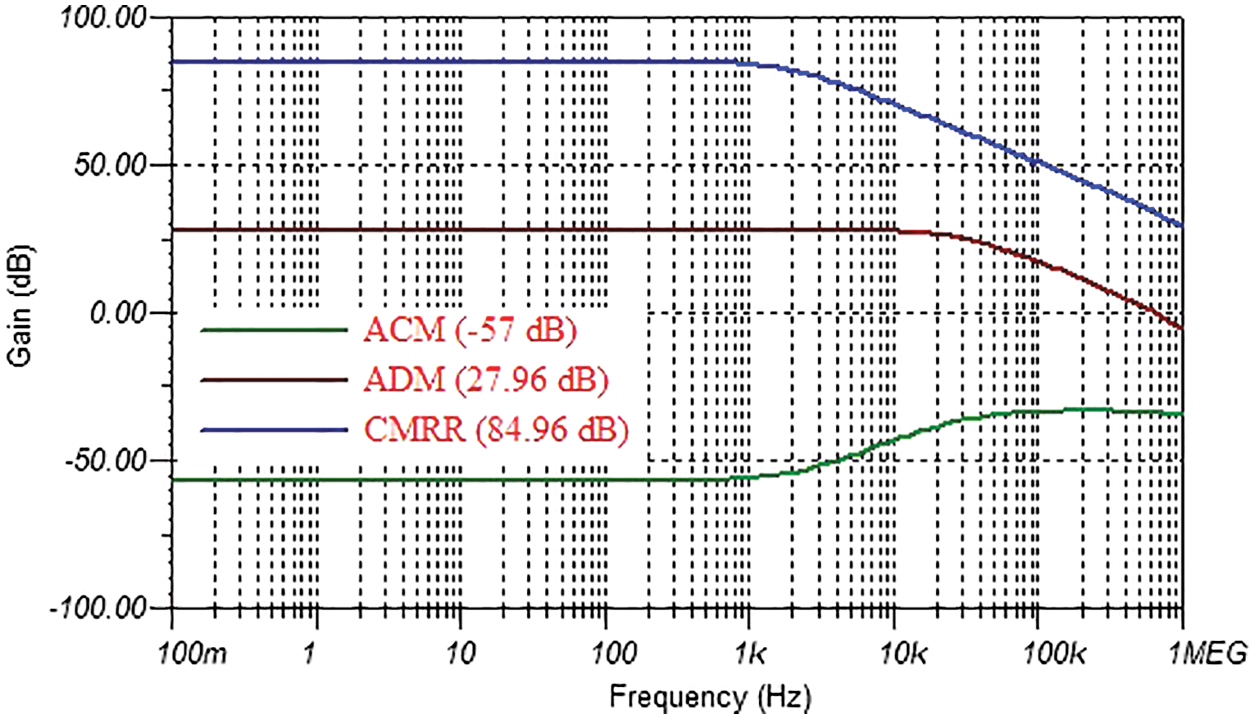
Figure 10: CMRR response of Op-Amp with nominal gain resistance values
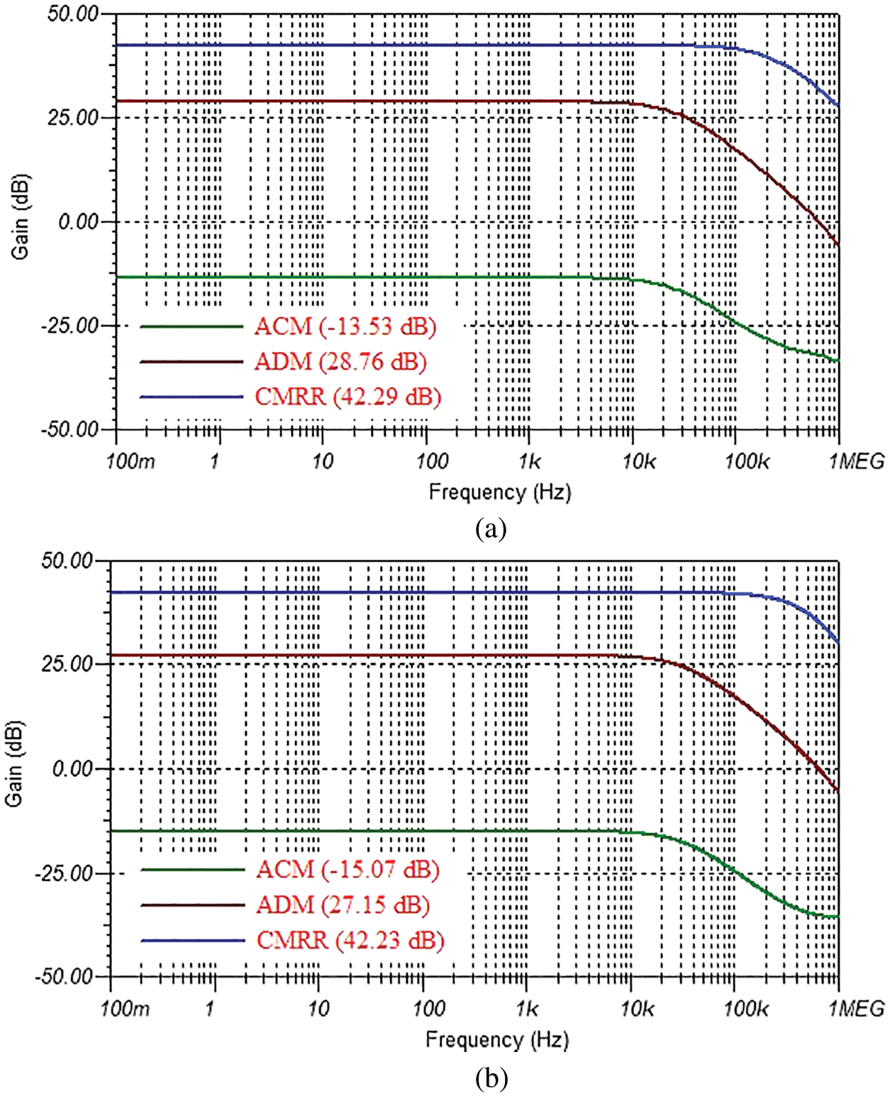
Figure 11: CMRR response of Op-Amp for gain resistors with 5% tolerance: (a) worst case maximum output voltage condition; (b) worst case minimum output voltage condition
By comparing the Fig. 11a response with ideal resistance condition the Common Mode Rejection Ration is reduced to 42.29 dB and less than half of the ideal condition. The common mode gain also decreased to −13.53 dB which effects in overall CMRR reduction. The CMRR response for 5% tolerance minimum differential gain condition is given in Fig. 11b.
The CMRR value with 5% tolerance minimum differential gain condition is nearly equal to the 5% tolerance maximum differential condition. In this case the common mode gain is improved to −15.07 dB and due to the reduction in differential gain the net CMRR is maintained to 42.23 dB. With 5% tolerance resistance the differential mode gain variation is ± 0.8 dB with respect to the nominal, whereas common mode gain is varied by more than 40 dB with respect to the common mode gain with nominal resistance values. By comparing these results with op-amp output voltage variations it will gives the detailed picture of effect of CMRR and Common Mode gain in measurement accuracy.
In nominal resistance case the common mode gain nearly zero or equal to the Op-amp saturation level and the output only depends on differential gain. In later cases the domination of Common mode signal over differential parameters leads to measurement errors. The CMRR response with 1% gain resistance tolerance for maximum and minimum differential gain conditions is shown in Figs. 12a and 12b respectively. With 1% tolerance the CMRR for Maximum and Minimum differential gain condition lies among 56.58 dB to 55.95 dB and the common mode gain value lies around −28 dB range.
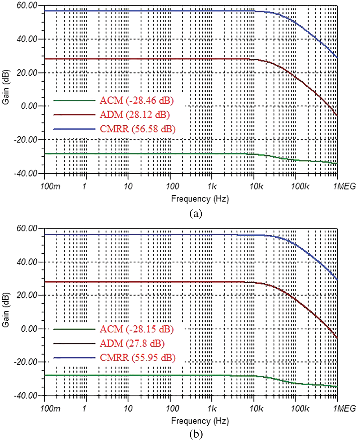
Figure 12: CMRR response of Op-Amp for gain resistors with 1% tolerance: (a) worst case maximum output voltage condition; (b) worst case minimum output voltage condition
By comparing these values with nominal resistance conditions shown in Fig. 10, the differential gain variation is ± 0.16 dB and Common mode gain variation is around 28 dB. The improvement is CMRR with 1% resistance tolerance reflects in output voltage and the error percentage is greatly reduced due to improved CMRR and Common Mode Gain.
The improvement in CMRR on reduction of Gain resistance tolerance to 0.5% is shown in Fig. 13. Based on Figs. 13a and 13b data the CMRR with 0.5% resistance tolerance is lies between 61 to 63 dB range. The variation in differential mode gain with respect to nominal differential mode gain is ±0.08 dB and the variation in common mode gain is around 22 to 23 dB range.
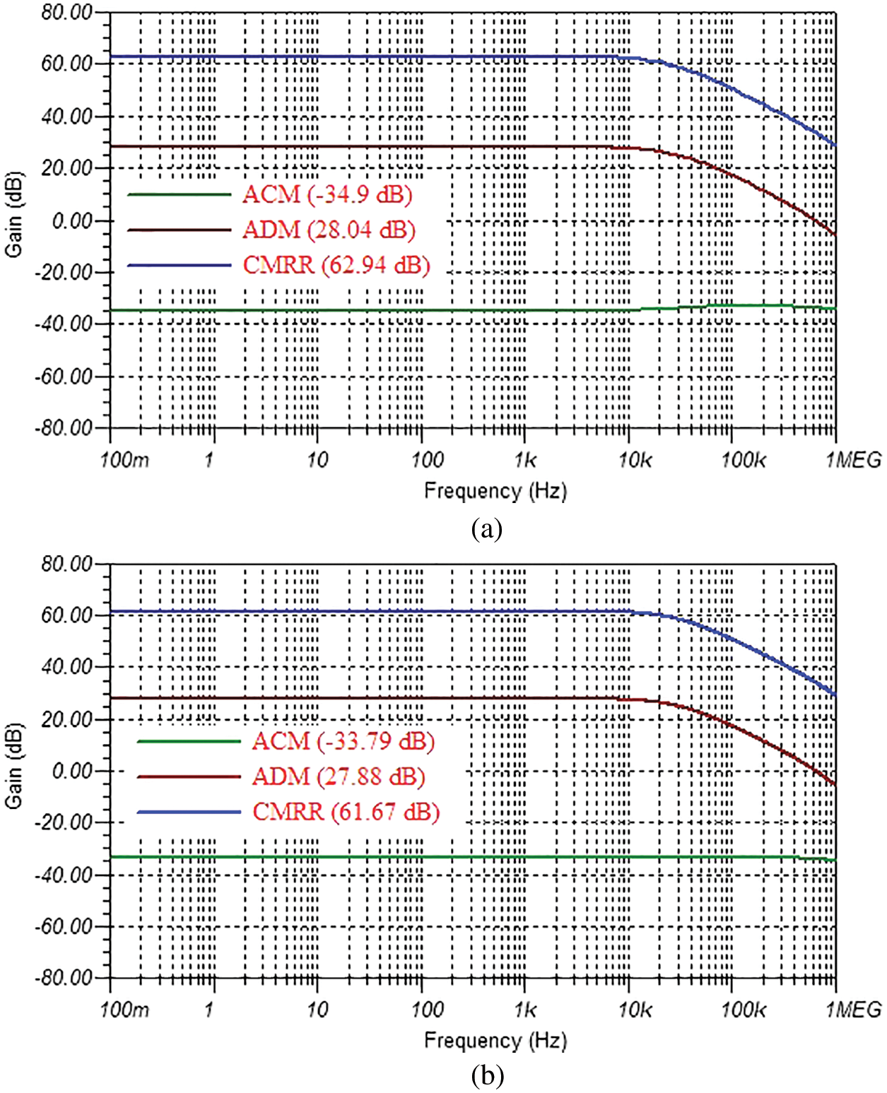
Figure 13: CMRR response of Op-Amp for gain resistors with 0.5% tolerance: (a) worst case maximum output voltage condition; (b) worst case minimum output voltage condition
By analyzing the equivalent output voltage measurement for the given input current, the overall response and accuracy of the system is improved due to the use of 0.5% tolerance gain resistors compared to 5% and 1% tolerance resistance cases.
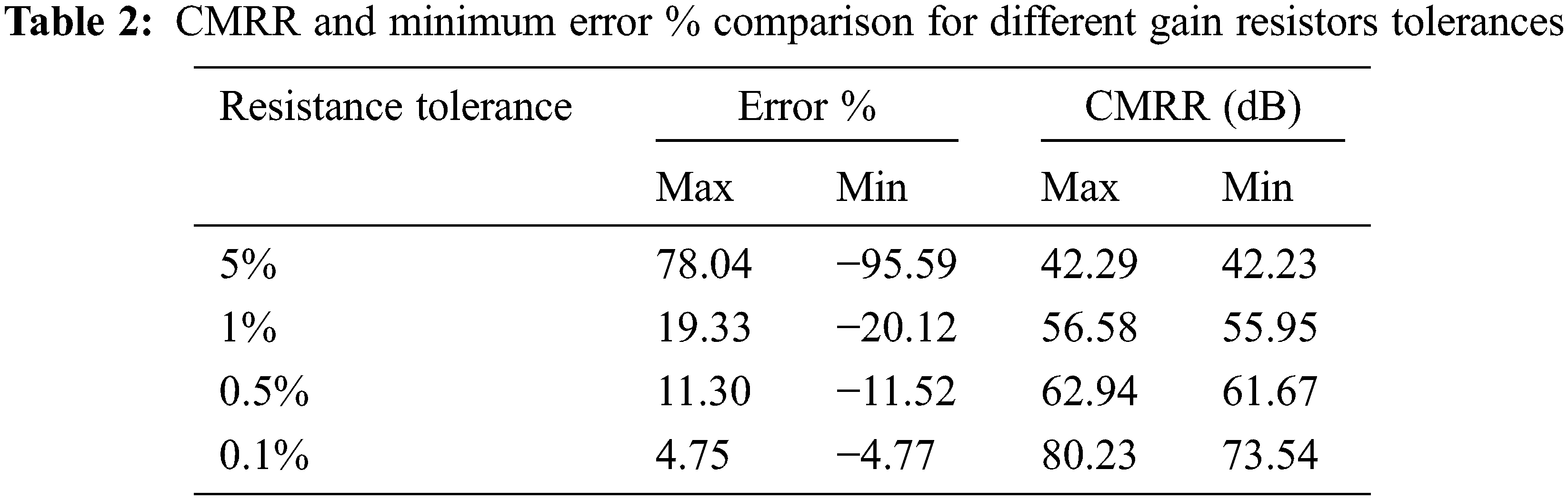
The CMRR and gain response analysis data with 0.1% tolerance resistors are given Fig. 14. For maximum differential gain condition, the CMRR of the differential Op-amp is 80.23 dB which is only around less than 4.5 dB than the nominal resistance CMRR value. The common mode gain value is −52.26 dB which is closer to the gain value with nominal resistance values. The CMRR value under 0.1% tolerance minimum differential gain condition is 73.54 dB. The output error percentage with respect to CMRR variations for different resistance tolerances are given in Tabs. 2 and 3.
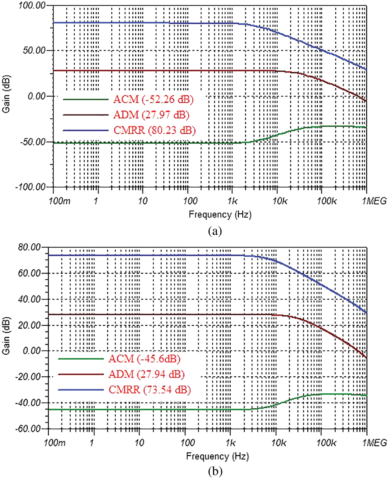
Figure 14: CMRR response of Op-Amp for gain resistors with 0.1% tolerance: (a) worst case maximum output voltage condition; (b) worst case minimum output voltage condition
4 Analysis of Op-Amp Offset Voltage Impact on Accuracy at Lower Magnitude Currents
Based on the Tabs. 2 and 3 data, the measurement error during low current condition is significantly higher than the error at high input current. The prior analysis with different tolerance resistors has done with the consideration of 3 mV Op-amp offset voltage. In low current input conditions, the Op-amp offset voltage plays a crucial role in determining output error and accuracy. The Op-amp offset voltage amplified based on the differential mode gain and added with the output voltage as an error component. The contribution of offset error component is equal in higher and lower current conditions. But, due to the low shunt resistor voltage the offset error contribution is dominant factor under lower current input conditions. In order to analyze the impact of Op-Amp offset voltage, the differential amplifier with 0.1% tolerance gain resistors taken for the consideration and the respective system performance is given in Figs. 7–9. With 3 mV offset voltage and 0.1% gain tolerance resistance the error percentage at 1A is 48.29% and −48.47% and improvements are needed to reduce this error percentage at lower current input condition.
The performance curve of the measurement system with 1 mV, 300 uV and 100 uV compared to 3 mV offset condition is shown in Fig. 15. These offset voltages are taken for analysis by considering the voltage across shunt for 1A input current which is 10 mV. From the Fig. 15, data with 1 mV offset voltage the net positive and negative error is reduce to ±28% from ±48% at minimum input current and also at maximum input current the error is reduced to ±2.7% from ±4.7%. The further reduction in offset voltage to 300 uV and 100 uV results is reduction of error percentage to ±21.4% and ±19.4% respectively for minimum input current condition. For maximum input current, the error is reduced to ±2.1% for 300 uV offset voltage and 1.9% percentage for 100 uV offset. In the above analysis the Op-Amp offset voltage considered as constant in order to find out the minimum and maximum worst case limits. However, the additional offset error occurs due to the variations in offset current at op-amp input terminals and based on input Common Mode voltage. In order to match the offset current at input terminals the gain resistor tolerances should be as low as possible and common mode voltage range should be selected based on the manufacturer recommendations to reduce the offset voltage effects. Other than that, in practical condition the Op-Amp offset voltage variation will depends on the operating temperature conditions too. So, based on the manufacturer recommendations the proper care should be taken while analyzing the offset impacts particularly at lower input current conditions.
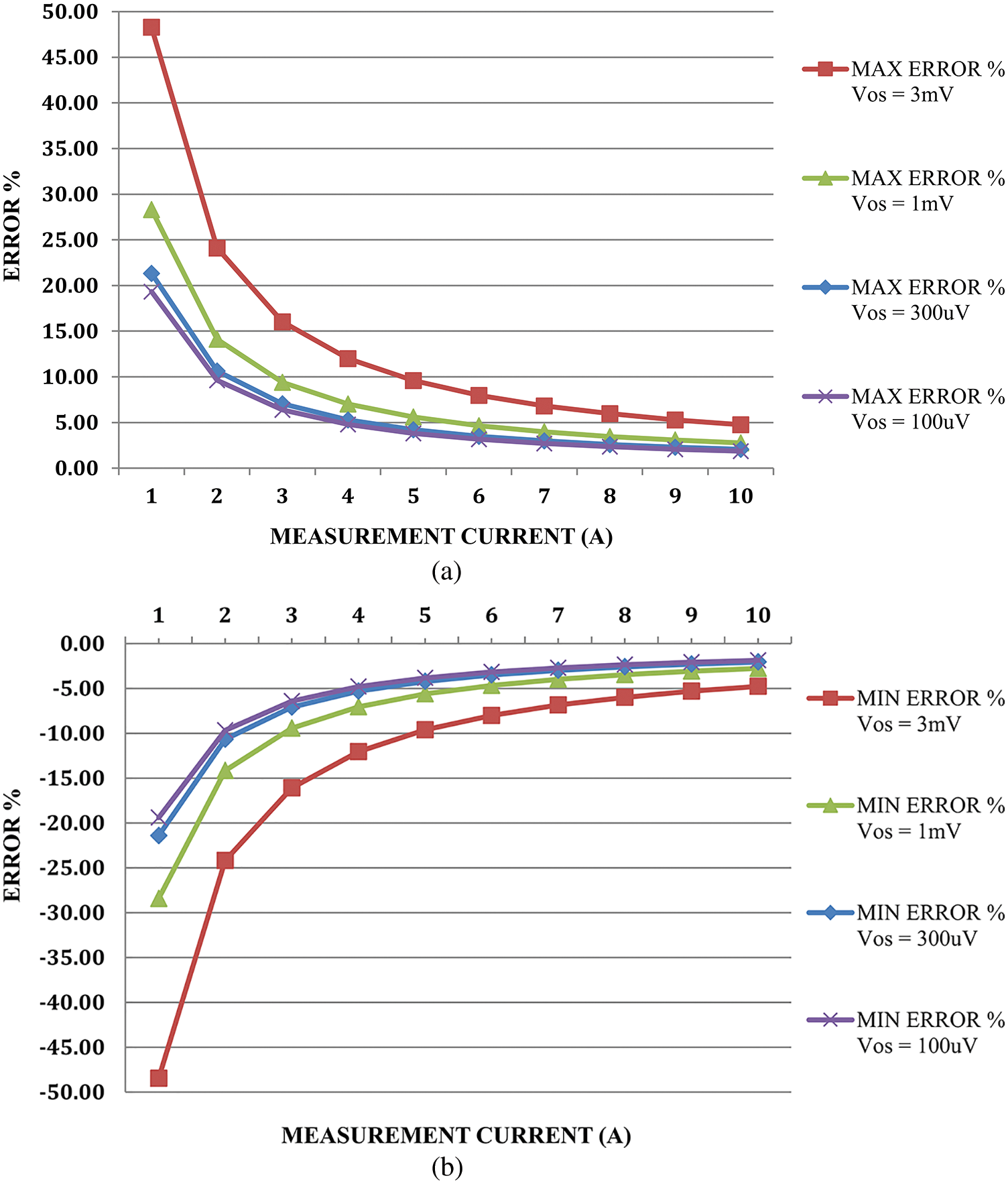
Figure 15: Worst case error percentages for Op-Amp with different offset voltages (vos) and 0.1% gain resistors tolerance: (a) maximum error; (b) minimum error
In this paper, the output accuracy analysis of high side differential op-amp current sensing circuit with different tolerance gain resistors for buck converter current measurement is performed. The worst case calculated results are compared with the simulation results and evaluated with percentage error analysis. The Common Mode Rejection Ratio simulation is performed for differential Op-amp with different gain resistor tolerance values and the relation between Common Mode Rejection Ratio and the measurement error percentage are examined. Based on the analyses which are made with 5%, 1%, 0.5% and 0.1% gain resistance tolerances, the gain resistors with 0.1% percentage tolerance exhibits better performance compared to higher tolerance cases. The higher tolerance resistors also produce major impact in reduction of CMRR by increasing Common Mode gain and variation in differential gain comparatively less than the common mode gain variations. With lower tolerance resistors the impact of Op-Amp offset voltage particularly at low input current conditions also analyzed and verified with different op-amp offset voltage conditions. From the analysis we have observed that if the Op-Amp offset voltage is less than 1/100 of voltage across the shunt at minimum current condition than the error due to Op-Amp offset voltage at low current conditions can be greatly reduced. The results of the proposed work are very useful for the error analysis of differential Op-Amp based shunt resistor and Hall based current measurement systems. However, the proposed work entirely concentrates on variation of output voltage with respect to the Gain resistor manufacturing tolerances, Op-Amp offset voltage and all other circuit parameters made as constant. During practical implementation along with manufacturer tolerances the additional tolerances shall be added with the gain resistors due to temperature, aging and other external conditions. Along with that, the shunt resistance values, shunt resistance tolerance, Op-Amp differential mode gain, PCB layout and other converter system parameters also generate great impacts on final results and its accuracy. Our future work will focus on complete and detailed analysis of above mentioned parameters additional to this proper work with hardware implementation.
Acknowledgement: We would sincerely want to thank the peoples who are supported to do this work and reviewing committee for their estimable feedbacks.
Funding Statement: The authors received no specific funding for this study.
Conflicts of Interest: The authors declare that they have no conflicts of interest to report regarding the present study.
1. A. C. Çalışkan, E. Kocaağa and C. Kasnakoğlu, “Average and peak current mode control comparison for full-bridge converter,” in 8th Int. Conf. on Electrical and Electronics Engineering (ICEEE), Antalya, Turkey, pp. 202–206, 2021. [Google Scholar]
2. J. Chen, Y. Hwang, J. Chen, Y. Ku and C. Yu, “A new fast-response current-mode buck converter with improved I2-controlled techniques,” IEEE Transactions on Very Large Scale Integration (VLSI) Systems, vol. 26, no. 5, pp. 903–911, 2018. [Google Scholar]
3. D. Tzelepis, V. Psaras, E. Tsotsopoulou, S. Mirsaeidi, A. Dyśko et al., “Voltage and current measuring technologies for high voltage direct current supergrids: A technology review identifying the options for protection, fault location and automation applications,” IEEE Access, vol. 8, pp. 203398–203428, 2020. [Google Scholar]
4. M. Biglarbegian, S. J. Nibir, H. Jafarian and B. Parkhideh, “Development of current measurement techniques for high frequency power converters,” in IEEE Int. Telecommunications Energy Conf. (INTELEC), Austin, TX, USA, pp. 1–7, 2016. [Google Scholar]
5. Y. Zhao, Z. Li, S. Yang, Z. Sun, Y. Yang et al., “Analysis of SenseFET performance degradation under electric stress,” in 14th IEEE Int. Conf. on Solid-State and Integrated Circuit Technology (ICSICT), Qingdao, China, pp. 1–3, 2018. [Google Scholar]
6. R. Pajer, M. Rodič and M. Milanovič, “Evaluation of MOS-FET RDSon resistance for current measurement purposes in power converter’s applications,” in Int. Conf. on Electrical Drives and Power Electronics (EDPE), Tatranska Lomnica, Slovakia, pp. 503–508, 2015. [Google Scholar]
7. S. Tian, W. Ballar, X. Chen, Y. Yan, Z. Liu et al., “A novel DCR current sensing scheme for accurate current read back in power umodule applications,” in IEEE Applied Power Electronics Conf. and Exposition (APEC), New Orleans, LA, USA, pp. 2763–2765, 2020. [Google Scholar]
8. Y. Yan and E. Gu, “A scalable multiphase current-mode buck controller with sub-milliohm DCR current sensing and synchronized overcurrent protection,” IEEE Journal of Solid-State Circuits, vol. 56, no. 9, pp. 2748–2759, 2021. [Google Scholar]
9. S. Ziegler, H. H. C. Iu, R. C. Woodward and L. J. Borle, “Theoretical and practical analysis of a current sensing principle that exploits the resistance of the copper trace,” in IEEE Power Electronics Specialists Conf., Rhodes, Greece, pp. 4790–4796, 2008. [Google Scholar]
10. B. Lu, X. Chen, J. Zhang, X. Wang and C. Ding, “Design of wide-range current transformer based on improved zero magnetic flux and turns compensation,” in 6th Asia Conf. on Power and Electrical Engineering (ACPEE), Chongqing, China, pp. 1267–1271, 2021. [Google Scholar]
11. P. Ripka, K. Draxler and R. Styblikova, “DC-Compensated current transformer,” in Proc. IEEE Int. Instrumentation and Measurement Technology Conf. (I2MTC), Montevideo, Uruguay, pp. 212–215, 2014. [Google Scholar]
12. M. G. Wath, P. Raut and M. S. Ballal, “Error compensation method for current transformer,” in IEEE 1st Int. Conf. on Power Electronics, Intelligent Control and Energy Systems (ICPEICES), Delhi, India, pp. 1–4, 2016. [Google Scholar]
13. Z. Jun, W. Liqun, C. Xuefei and J. Yi, “Research and design of a new type of high current bidirectional hall current sensor,” in IEEE Asia Conf. on Information Engineering (ACIE), Sanya, China, pp. 82–85, 2021. [Google Scholar]
14. Z. Liu, “Overview of hall current sensor optimal design,” in IEEE Int. Conf. on High Voltage Engineering and Application (ICHVE), Beijing, China, pp. 1–4, 2020. [Google Scholar]
15. A. D. Saha and V. John, “Power consumption reduction in high current closed loop hall effect current sensors using class D amplifier,” in IEEE Int. Conf. on Power Electronics, Drives and Energy Systems (PEDES), Thiruvananthapuram, India, pp. 1–6, 2016. [Google Scholar]
16. M. Ben-Esmael, B. L. Hart, K. Hayatleh and F. J. Lidgey, “CMRR-Bandwidth extension technique for CMOS differential amplifiers,” AEU-International Journal of Electronics and Communications, vol. 68, no. 10, pp. 990–993, 2014. [Google Scholar]
17. G. Hornero, O. Casas and R. P. Areny, “Common mode response effects in differential measurements,” AEU-International Journal of Electronics and Communications, vol. 128, pp. 152510, 2021. [Google Scholar]
 | This work is licensed under a Creative Commons Attribution 4.0 International License, which permits unrestricted use, distribution, and reproduction in any medium, provided the original work is properly cited. |