DOI:10.32604/iasc.2023.027650
| Intelligent Automation & Soft Computing DOI:10.32604/iasc.2023.027650 | |
| Article |
Fin Field Effect Transistor with Active 4-Bit Arithmetic Operations in 22 nm Technology
1Department of Electronics and Communication Engineering, SRM Valliammai Engineering College, Chennai, 603203, India
2Department of Electronics and Communication Engineering, College of Engineering Guindy, Anna University, Chennai, 600025, India
*Corresponding Author: S. Senthilmurugan. Email: Senthilmurugan.ece@outlook.com
Received: 22 January 2022; Accepted: 01 March 2022
Abstract: A design of a high-speed multi-core processor with compact size is a trending approach in the Integrated Circuits (ICs) fabrication industries. Because whenever device size comes down into narrow, designers facing many power density issues should be reduced by scaling threshold voltage and supply voltage. Initially, Complementary Metal Oxide Semiconductor (CMOS) technology supports power saving up to 32 nm gate length, but further scaling causes short severe channel effects such as threshold voltage swing, mobility degradation, and more leakage power (less than 32) at gate length. Hence, it directly affects the arithmetic logic unit (ALU), which suffers a significant power density of the scaled multi-core architecture. Therefore, it losses reliability features to get overheating and increased temperature. This paper presents a novel power minimization technique for active 4-bit ALU operations using Fin Field Effect Transistor (FinFET) at 22 nm technology. Based on this, a diode is directly connected to the load transistor, and it is active only at the saturation region as a function. Thereby, the access transistor can cutoff of the leakage current, and sleep transistors control the flow of leakage current corresponding to each instant ALU operation. The combination of transistors (access and sleep) reduces the leakage current from micro to nano-ampere. Further, the power minimization is achieved by connecting the number of transistors (6T and 10T) of the FinFET structure to ALU with 22 nm technology. For simulation concerns, a Tanner (T-Spice) with 22 nm technology implements the proposed design, which reduces threshold voltage swing, supply power, leakage current, gate length delay, etc. As a result, it is quite suitable for the ALU architecture of a high-speed multi-core processor.
Keywords: FinFET (22 nm) technology; diode connection; arithmetic logic unit; reduce threshold voltage swing; gate length delay; leakage power
Today, the ICs fabrication industry is mainly focused on scaling the device factor (<22 nm) technology which supports system on chip (SOC) engineers to bring their design innovation that’s show drastically growth of intelligent computers and mobiles. But a design challenge happens when the device size is scaled below 22 nm because applying proper scaling ratio with all the device parameters is challenging. Anyhow, the supply voltage is dominating factor for evaluating dynamic power utilization. Thereby, it is a predominant factor always encountered at any scaling technology. Hence, it is necessary to have transistor structure modeling that brings new revolutionary growth in the CMOS technology.
Moreover, [1] Moore’s law stated that the transistor occupancy is double for every consequent year. To fulfill this, the Metal Oxide Semiconductor (MOS) transistor came into the IC fabrication, and it has potential benefices of high performance over compact device size. However, the device scaling factor gets exhausted after a specific threshold limit and thus, faces a considerable power leakage problem. Therefore, the double gate terminal transistor (Frontside and Backside) is evolved to resolve the power issues by reducing gate length [2]. Hence, it has highly influenced the modern PCs framework due to its device structure modeling. Because the bias voltage of gate terminal (backside) is adjusted, minimizing the amount of leakage current flow by setting appropriate sub-threshold voltage. It conveys that if the transistor is operated in the saturation region, it has consumed more power than the sub-threshold point. Usually, scaled transistors suffer short channel effects (SCE), threshold voltage swing, gate oxide burrowing spillage, etc. [3].
Once the device scaling is completed, now, it would analyze the power efficiency of such transistors by testing its arithmetic operations. In general, the arithmetic logic unit (ALU) is the primary unit of any processor that performance addition, subtraction, multiplication, division, etc. These operations are executed through a single cell unit, which significantly reduces the chip area’s occupancy. Initially, ALU is fully implemented with Metal Oxide Semiconductor Field Effect Transistor (MOSFET) technology but conflicts few issues related to SCE and oxide spillage. Later, ALU is planned with a FinFET [4]. The logical function includes a comparator, modulus, and other arithmetic operations using an 8-bit ALU structure on MOSFET with 65 nm technology. It supports high-speed multi-tasking but suffers a considerable amount of power leakage. This is because of interconnection shortage and limited gate thickness.
Usually, MOSFET has bulk power leakage due to self-warming, soft error rate, strained-Si channel, and high-K gate [5]. To overcome such complaints, FinFET is involved, a multi-gate gadget that reduces gate delay threshold swing and minimizes leakage current spillage [6]. A 1-bit ALU is designed at 32 nm FinFET technology, which improves average power consumption and achieves reasonable operation speed [7]. The low-power digital CMOS circuits require a unique transistor configuration style that allows efficient power utilization and minimized gate delay accompanied by a few transistors [8]. This paper presents a novel power minimization technique for active 4-bit ALU operations using FinFET at 22 nm technology. Based on this, a diode is directly connected to the load transistor, and it is active only at the saturation region as a function. Thereby, the access transistor can cutoff of the leakage current, and sleep transistors control the flow of leakage current corresponding to each instant ALU operation. The section detail of this paper is given as follows: Section 2 describes the related work on ALU designing using FinFET technology. A basic ALU design with various modes of implementation is discussed in Section 3. A diode-connected sleep transistor for power minimization in the 4-bit ALU operation is presented in Section 4. The schematic and simulation results of the arithmetic and logical operations of the ALU are discussed in Section 5. Finally, and the conclusion is made in Section 5.
A multi-gate gadget using CMOS technology [9] to incorporate innovative ICs fabrication. It is the structural ability to convert a single gate device into a multi-gate device (double and triple). Hence, it suffers a lack of power utility and leakage. Even though the scaling factor retains the transistor switching characteristic, it loses the functional efficiency due to leakage power. Therefore, it has occupied a significant part in the total power supply of the FinFET logic circuits. It mainly deals with the various power-saving modes of FinFET logic styles. A gate voltage is controlled effectively by adjusting the sub-threshold voltage appropriately. Hence, the power utility factor is improved by double the rate compared with traditional CMOS technology.
A Full adder circuit design using (32 nm) FinFET technology with 28 control transistors [10], and results are compared with MOSFET and FinFET technology, respectively. It conveyed that the FinFET takes a 50% improvement in power saving capability compared with MOSFET. Because FinFET is an easy fabrication process on a CMOS transistor, average power consumption and gate delay are reduced exponentially.
A design of latches and flip-flops using independent gate (IG) FinFET for minimizing power consumption and area occupancy [11]. Hspice simulator tool is used for experimental purposes. A result shows that the proposed design has reduced the active power consumption (47%), the clock power (32%), the leakage power (42%), and the circuit area (20%) concerning 32 nm FinFET technology. But, it has maintained similar operation speed and circuit stability. In this regard, gate terminal voltage is adjusted up to sub-threshold limits, thus reducing power dissipation by minimizing the capacitance between drain and source terminal. Anyhow, it is not sufficient and suitable for large-scale IC fabrication.
An analytical model for estimating the logical circuit [12] performance using low-power independent gate-based FinFETs. According to this, a separate logical library function is developed to replicate the actual testing of FinFET for ALU operation. The experimental results conveyed that the chip area occupancy of 8.5% and power utility factor of 18% improvement reached over conventional 45 nm FinFET technologies.
A novel bottom spacer-based [13] FinFET structure suitable for logic operation and easy convents into system-on-chip (SoC) requirements. It mainly focuses on improving power utility factors in the presence of short channel effect, gate delay, and self-heating compared with traditional FinFET (silicon-on-insulator type).
The designing challenging issues faced on scaling MOS transistors [14]. The scaling factor should not affect the device parameters like supply power, threshold voltage, gate delay, fluctuation, and parasitic capacitance. The nano-scaling traditional brings a new revolutionary on transistor structure and ICs fabrication.
A one-bit sum and carry adder circuit using cadence Virtuoso at 180 nm technology. This paper compares power-saving and utility factors with conventional CMOS technology. The operation speed and propagation delay are reduced with the help of short gate length. The gate voltage is controlled by fixing a sub-threshold voltage from the supply voltage. Thereby, power consumption and self-heating are minimized as compared with CMOS design.
The energy consumption of Power Clock Generator (PCG) at the 90 nm CMOS technology. It involves an adiabatic circuit/system that effectively handles the power variation at transistor depth and process deviation. It contains a two-stage comparator that generates the difference output as a single cycle clock signal. The simulation result is compared with a 4-bit adiabatic Ripple Carry Adder (RCA) and inferred the clock frequency range from 20 MHz to 1.5 GHz. The proposed PCG gives a maximum conversion efficiency of 56.48%. This research work shows how the design of an efficient PCG increases the energy saving of adiabatic logic.
ALU is an essential functional block present in the central processing unit of any processor. It can perform all kinds of arithmetic (addition, subtraction, multiplication, and division) and logical (AND, OR, NOT, NAND, NOR, XOR) operations. Due to device scaling, gate length, threshold voltage, and leakage current levels are adjusted linearly by structure modification. As a result, the ALU circuit should not leave its operating speed and withstanding power density within the threshold limit. However, it is challenging to get scaled form through CMOS technology just below 32 nm, the reason that, suffers more power dissipation, large leakage current, threshold voltage swing, etc. But, it would be limited by implementing ALU on 22 nm FinFET technology. Hence, it highly supports high-speed ALU operation with minimum power constraints. According to this, the functional block is the same as the basic ALU standard. Here, it introduces different levels of the transistor, and it could be operated into four different modes, namely Short Gate (SG), Independent Gate (IG), Low Power (LP), and Hybrid IG/LP.
In this mode, the transistor channel length is controlled by shorted gate terminal of the FinFET. By the way, it reduces the voltage swinging and takes less power to encapsulate the ALU operation. Fig. 1 shows the circuit implementation of SG mode design using (a) inverter type (b) NAND logical.
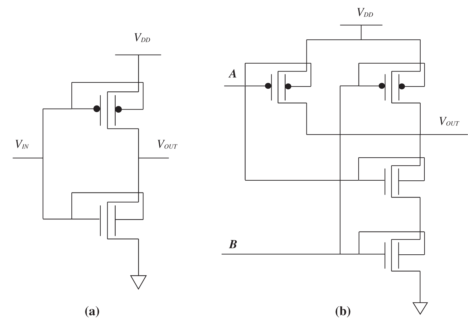
Figure 1: Design of SG mode circuit (a) inverter type (b) NAND logical
It is the suitable mode to reach minimum power density by giving appropriate voltage biasing at the input of the gate terminal of the transistor. That means the gate terminal is biasing like a −0.5 V (low voltage) is given to n-type and 1.5 V (high voltage) is given to p-type of FinFET transistor, respectively. As a result, the threshold voltage is controlled with delay induction that reduces leakage power dissipation. Fig. 2 shows the circuit implementation of LP mode design using (a) inverter type (b) NAND logical.
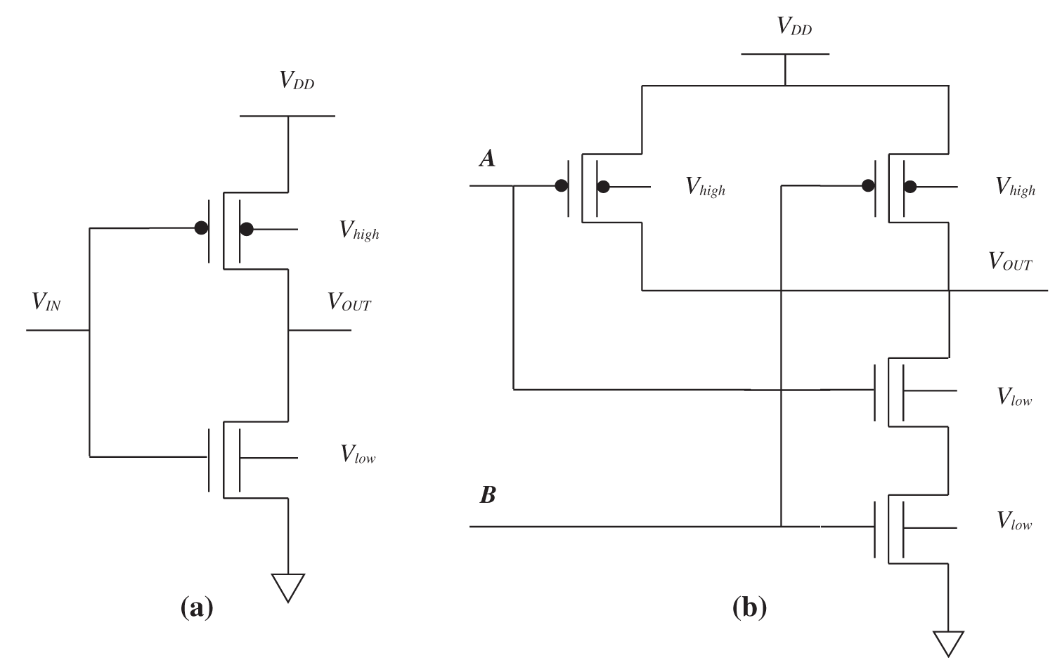
Figure 2: Design of LP mode circuit (a) inverter type (b) NAND logical
According to this mode, the number of transistor usage at the ALU operation is minimized. That is, two independent input signals are applied to p-type. One signal is directly connected to the front gate, and the other is connected to the back gate terminal. But, the n-type is maintains shorted terminal as similar to SG mode. Fig. 3 shows the circuit implementation of IG mode design using (a) inverter type (b) NAND logical.
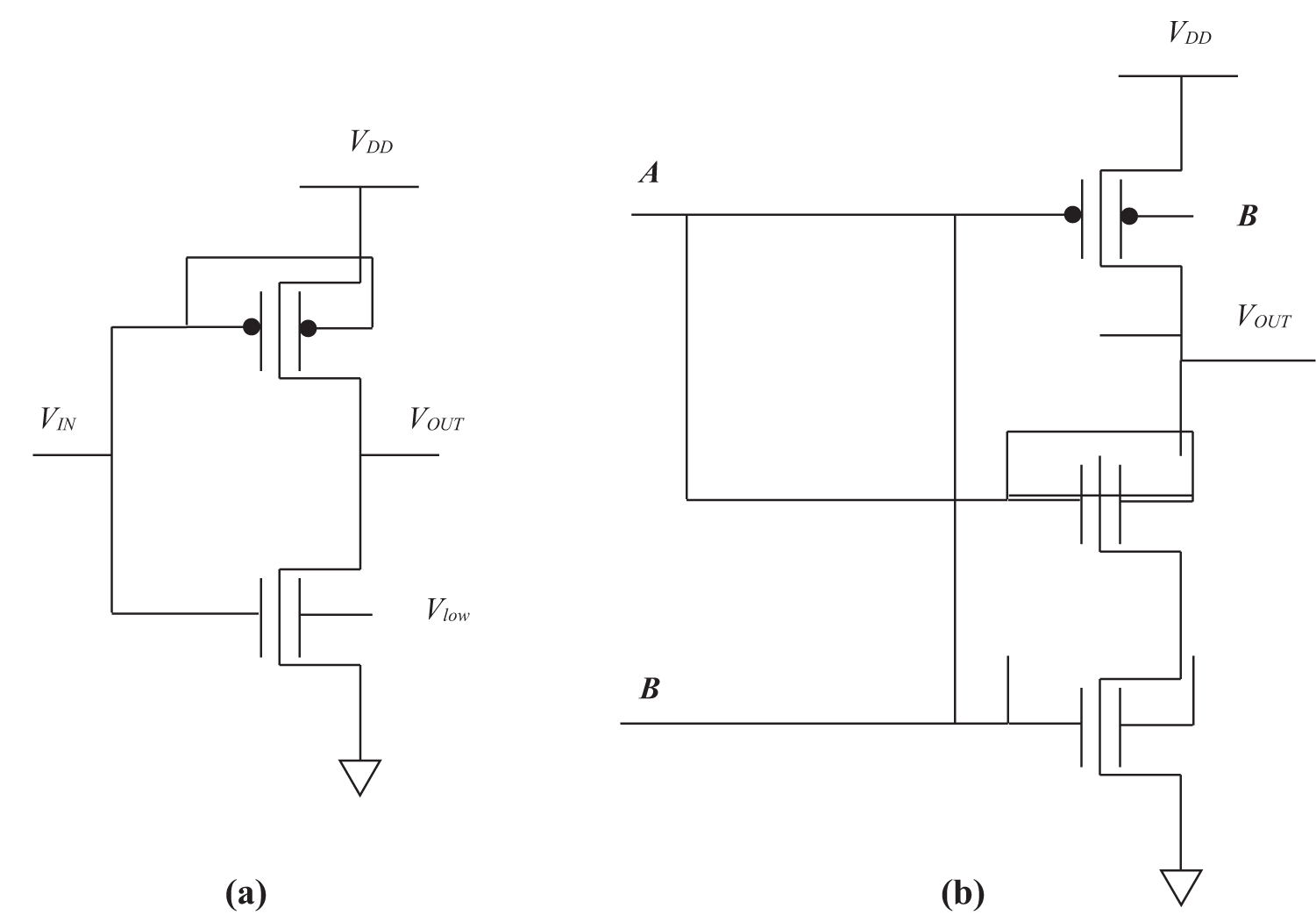
Figure 3: Design of IG mode circuit (a) inverter type (b) NAND logical
It combines both LP and IG modes linearly connected. In this mode, leakage current and voltage swinging are reduced with increased delay due to signal shorting at the n-type transistor.
4 Design of Proposed 4-bit ALU Circuit
In general, a logical operation is carried out by the Arithmetic logic unit (ALU), and its function is sequential controlled with the selection line of the multiplexer. In this paper, a 4-bit ALU circuit is implemented using Tanner (T-Spice) with at 22 nm FinFET technology. Fig. 4 shows the block diagram of the proposed 4-bit ALU design. It consists of 4 multiplexers (8:1 MIX) and 4 adders (2-bit adder), which perform different logical operations (AND, OR, NOT, NAND, NOR, XOR, comparator, and modulo 2 addition). According to function-specific, the 4-outputs of the multiplexer have been obtained. The proposed design is made up of n and p-type FinFET transistors.
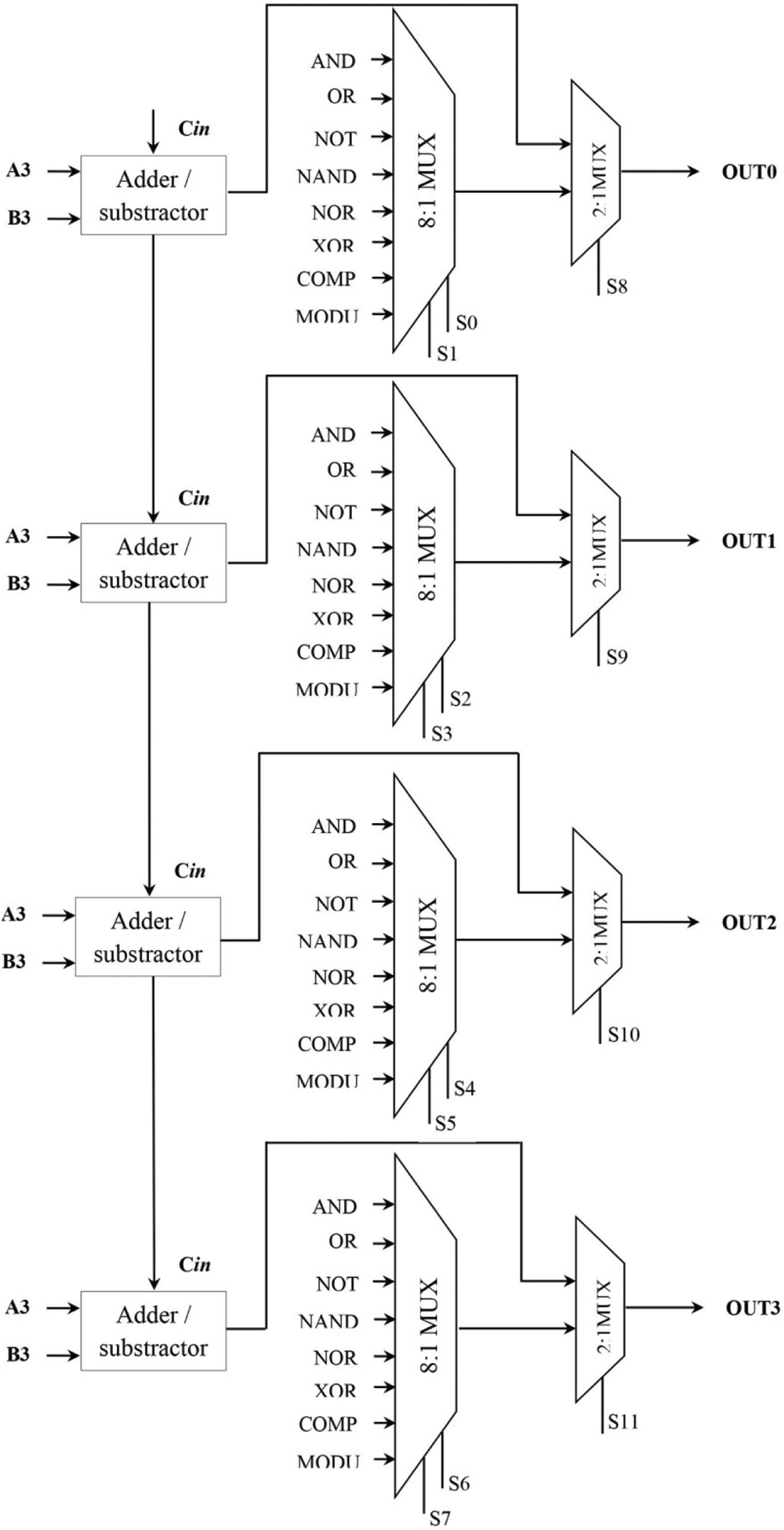
Figure 4: Block diagram of proposed 4-bit ALU design
It is a primary function required for completing the specific digital task of any processor. It is a derived study of numerical calculus and number theory. The high-level operations are categorized into high and low priority, including Vedic mathematics, Boolean algebra, trigonometry function, and complex analysis. In the scaling perspective, comparator (<, > and <= or >=) and modulo 2 addition is highly prioritized to complete the specific task in a much faster manner. It has come under the elementary part of the analysis and sustains advanced mathematic operation within time constraints.
The gate is made up of an electronic device that provides logical validation at the output terminal by following different combinations of inputs. Usually, gate circuits are designed with more inputs rare than output terminals. That is, multiple inputs and one output, respectively. Using logical gates can design any combination or sequential circuits that interrupt ALU operations (AND, OR, NOT, NAND, NOR, XOR). The basic structure of the individual logical gate is replaced with 22 nm FinFET technology.
It is mainly used to combine many inputs into one single output. The selection line (MUX) is used to select the data lines that come out of the output. In the proposed design, consider four (8:1 MUX & 2:1 MUX) consequentially to speed up the ALU function and reduce the carry propagation delay.
4.4 4-Bit ALU Design Using Diode Connected Sleep Transistor
Power dissipation is a common problem in the scaled design of high-speed function ALU using FinFET technology. It is significantly reducing the performance efficiency of the ALU due to the large Leakage current that takes place in the transistor terminals. It must be limited by increasing the path resistance of the high leakage current flow. But it is not always to sustain the high resistive path of any scaled design. Thereby, the asleep transistor is used to give a resistor operation by connecting the gate and drain terminals of the MOS transistor. Such type of transistor is referred to as diode-connected sleep transistors. It is shown in Fig. 5. Because it exhibits diode function, it can turn on only if the transistor is in the saturation region. Otherwise, it remains off state to slow down the leakage current flow. That implies both P-Metal Oxide Semiconductor (PMOS) and N-Metal Oxide Semiconductor (NMOS) transistors can be made to act as Diode-connected transistors.
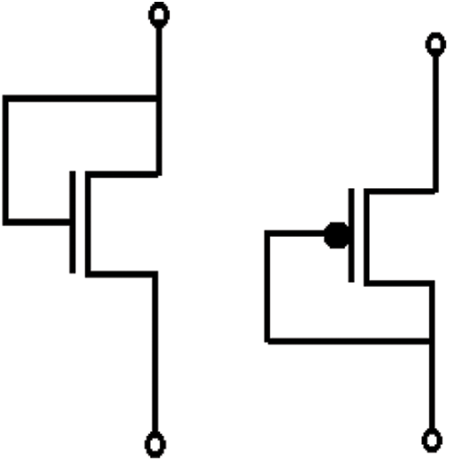
Figure 5: Diode connected sleep transistors
In the proposed 4-bit ALU design, NMOS acts as diode-connected sleep transistors that reduce considerable leakage current flow by operating the transistor to its minimum point. If the high input voltage is given to the sleep transistor, it remains in the off state. Thus, offers high resistance that blocks current flow to logical operator transistors. Meanwhile, in Figs. 6 and 7, if the low voltage is applied, the sleep transistor remains in the off state. Because it made shorted terminal through that discharge leakage current is grounded. These two main functions are extracting by placing a diode-based sleep transistor and establishing a constant with minimum leakage current.
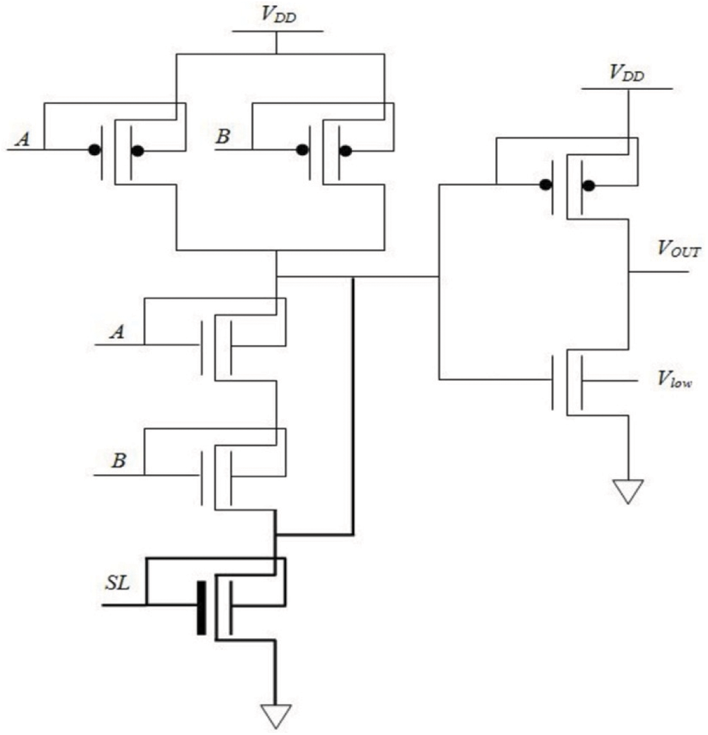
Figure 6: IG mode AND gate operation using Diode connected sleep transistors
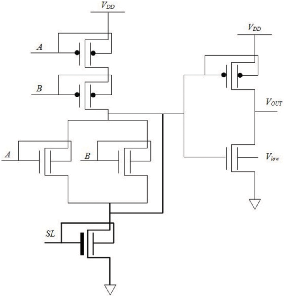
Figure 7: IG mode OR gate operation using Diode connected sleep transistors
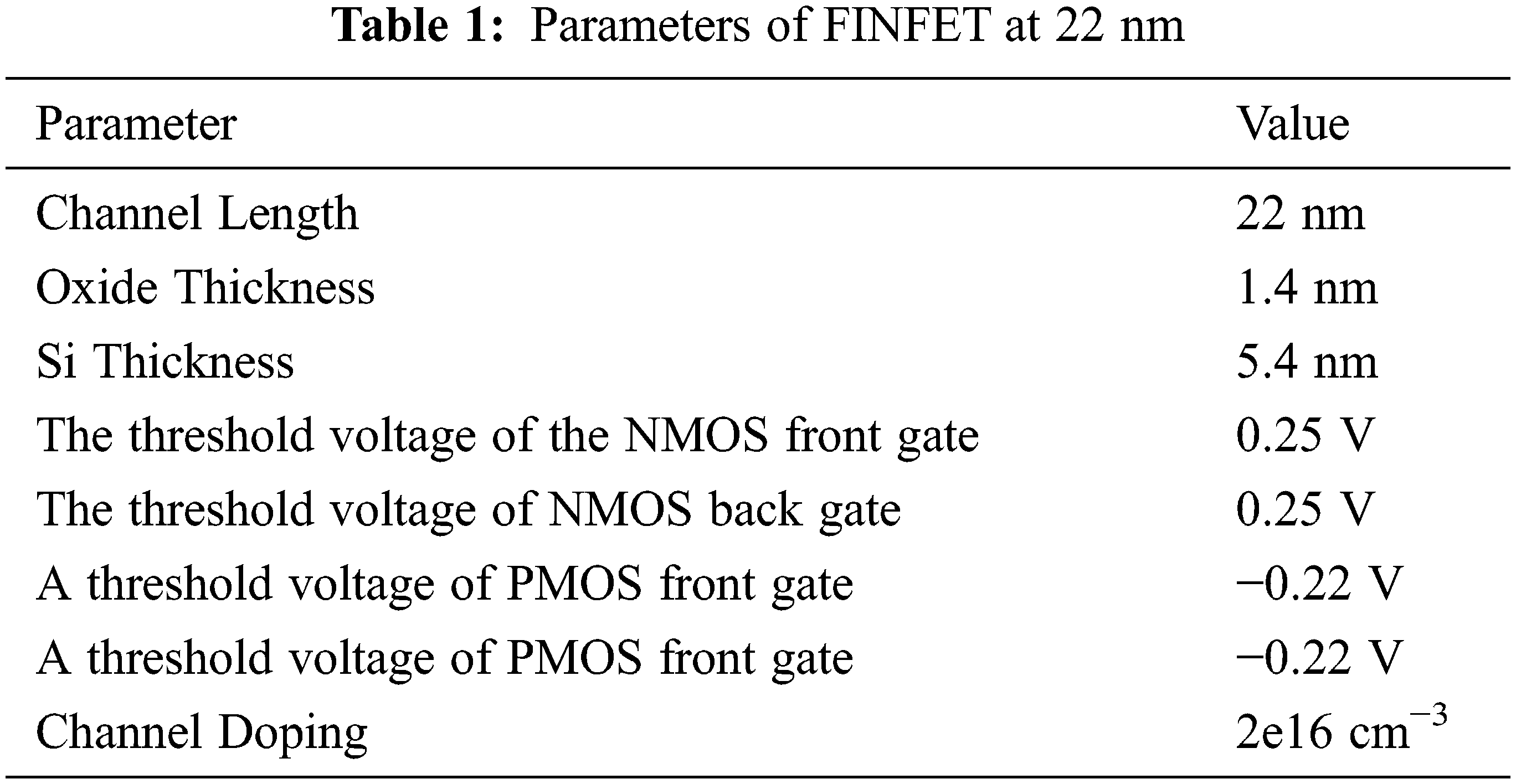
This section discusses the simulation result of the proposed 4-bit ALU design using FinFET technology. It is implemented by using the HSpice tool in 22 nm technology. The modeling parameters of FinFET at 22 nm are shown in Tab. 1.
The Independent gate of the FinFET technique is chosen for the proposed 4-bit ALU design since it has only average power consumption. This has been proved by comparing different FinFET modes with diode-connected sleep transistors, which concluded that the proposed method consumes less power and has better arithmetic and logical operation stability. Tab. 2 illustrates the average power consumption of the proposed method and CMOS transistor.
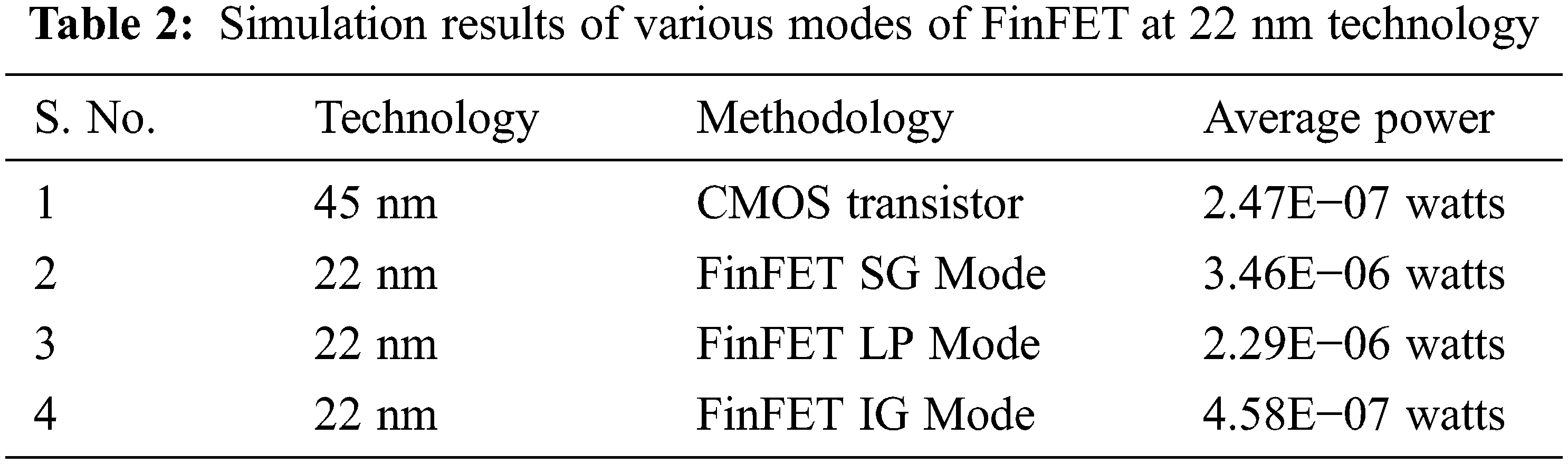
In the power minimization analysis, the independent gate mode is superior to the other three FinFET technology modes. The average consolidation of leakage power and leakage current of the SG, LP, and Hybrid modes is simulated, seen as 28.64 nW and leakage current as 135.24 pA, respectively. The proposed method is implemented in the independent model for overcoming this leakage issue. The simulation result of independent gate mode 4-bit ALU using diode-connected sleep transistor is simulated, and leakage power is seen as 6.15 nW and leakage current as 42.85 pA. It is shown in Fig. 8.
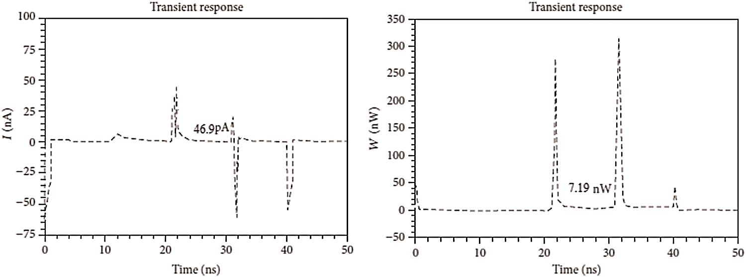
Figure 8: Leakage current and leakage power consumption of the proposed technique
The three inputs Full Adder circuit is implemented and simulated using the HSpice tool in 22 nm technology. The result is compared with Full Adder circuit design at CMOS (45 nm) and FinFET (22 nm) technology. Tab. 2 offers a comparison between the delay and power of the Full Adder circuit for 45 nm and 22 nm technology with 1 V VDD. The table provides information relating to the different input vectors of the Full Adder circuit. Leakage power obtained mainly depends on the input vector and applying Diode connected sleep transistor. It effectively reduces leakage power compared to CMOS (45 nm) and FinFET (22 nm) without a sleep transistor. The power-delay-product (PDP) for dynamic and static power where the proposed 4-bit ALU with Diode connected sleep transistor is much better for static power but a smaller power variation in dynamic due to addition of transistor in this model. It is indicated in Tab. 3. Thus, it conveys that the delay is minimized as low as possible compared with CMOS (45 nm) and FinFET (22 nm) without a sleep transistor.
Similarly, the parameters like leakage power PDP of dynamic and static power are estimated, which is much lower when compared to other methods with 0.85 V VDD. It is shown in Tab. 4. But, in delay, it is slightly higher in CMOS (45 nm) and lower in FinFET (22 nm) without a sleep transistor. Tab. 5 shows the delay and power comparison of the proposed method at 22 nm process technology with other techniques. The conventional CMOS technique has a lower dynamic power and a higher leakage power. The simulation results are shown in Figs. 9–13.
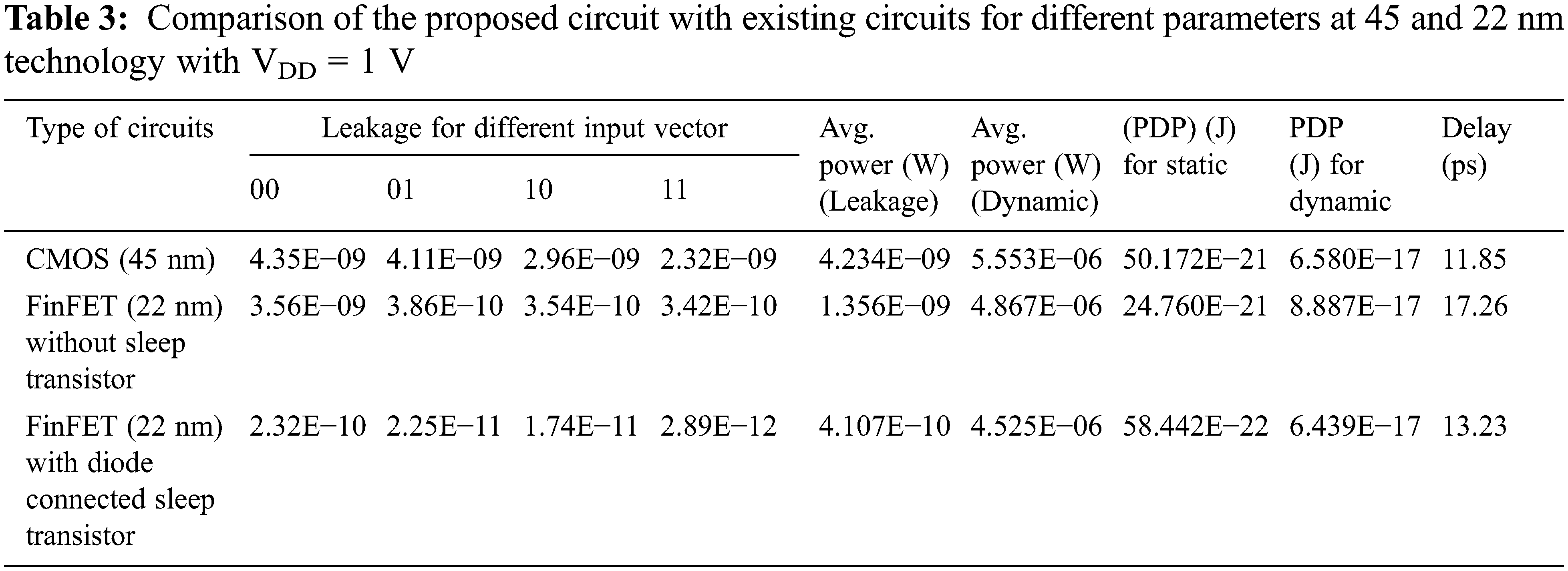
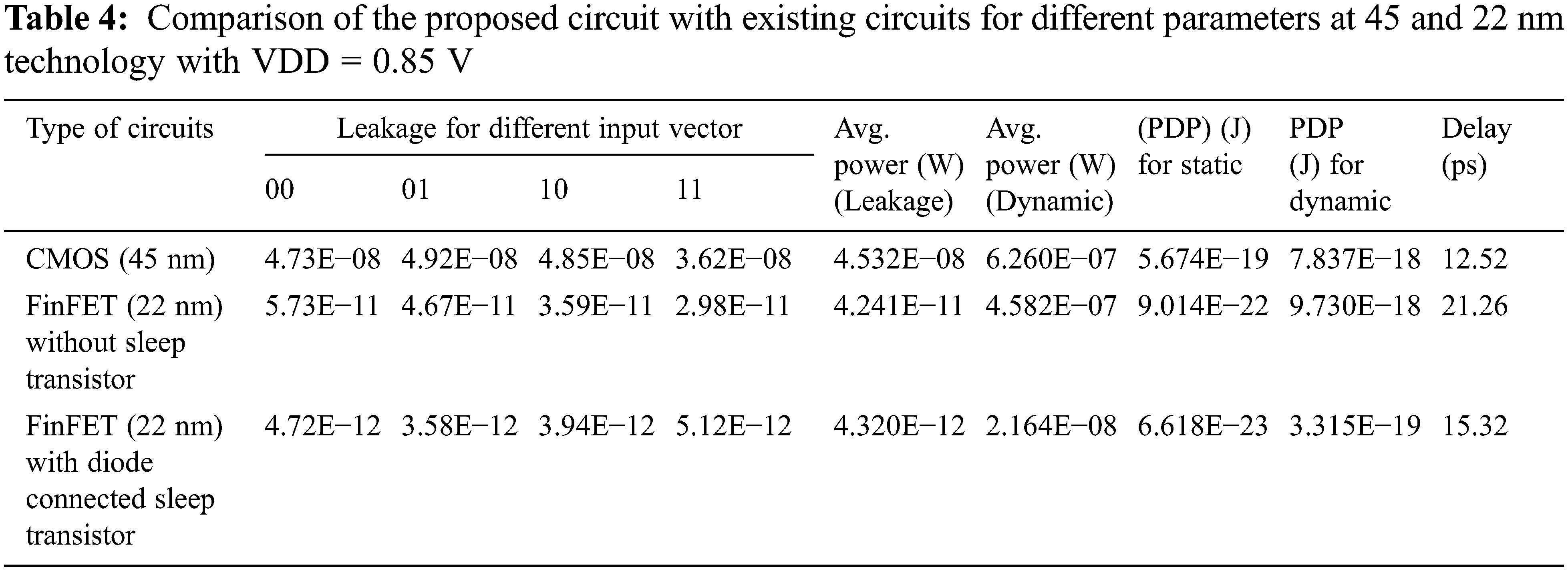
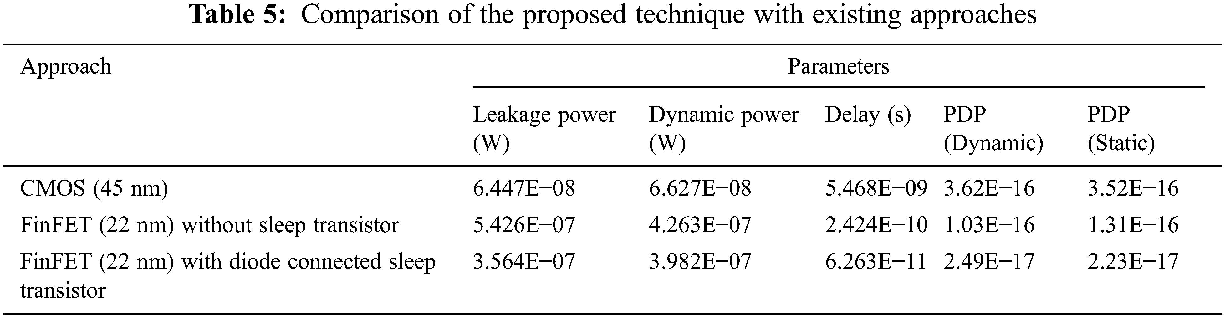
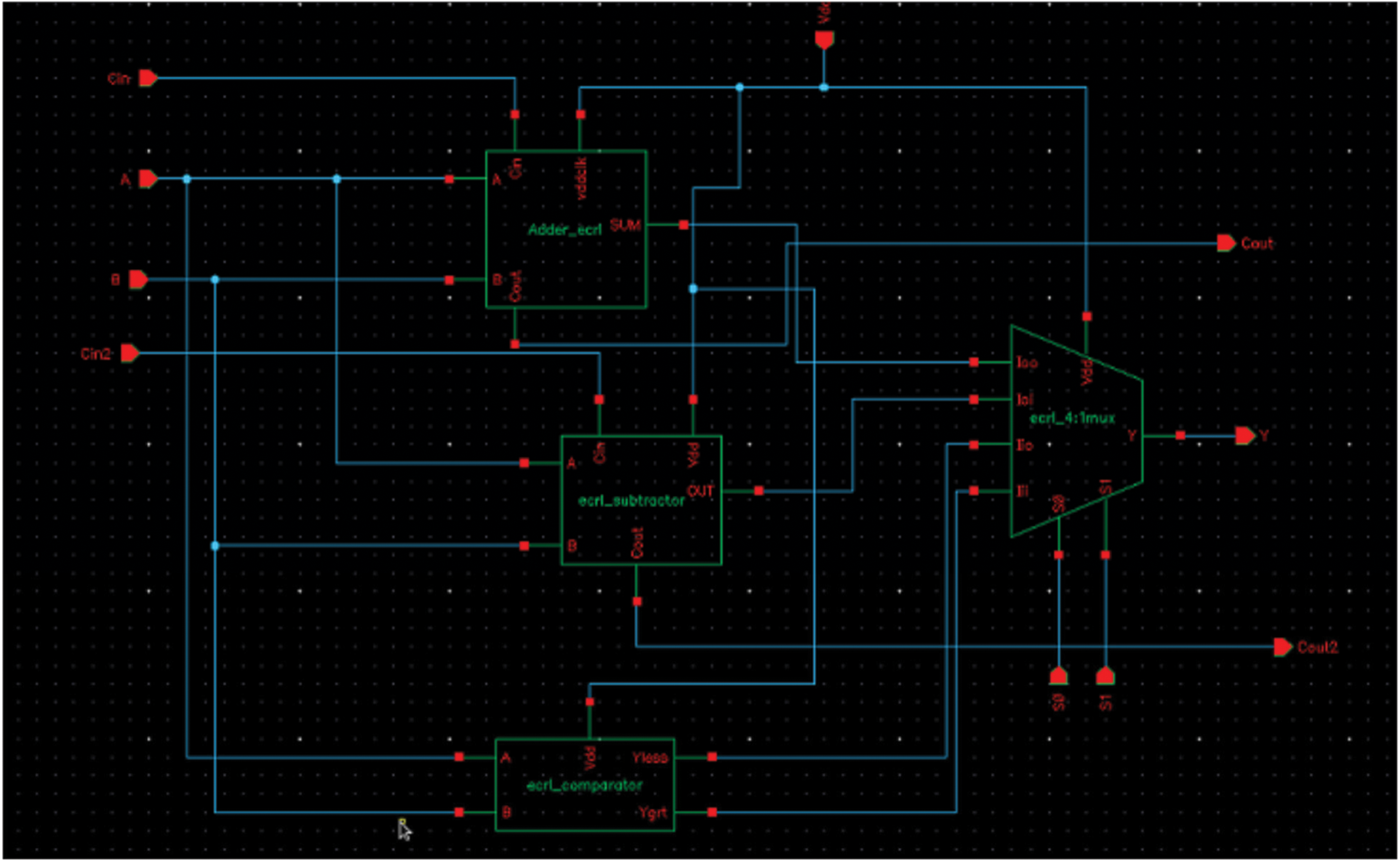
Figure 9: Design of arithmetic operation block
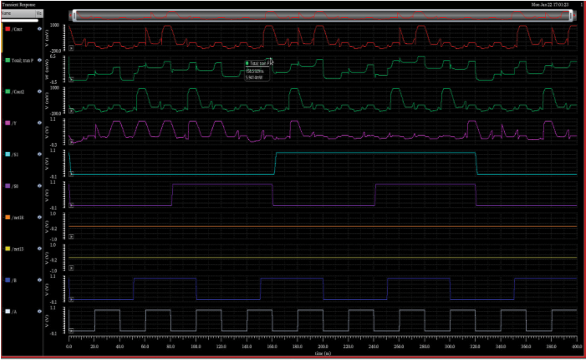
Figure 10: Simulation results of arithmetic operation block
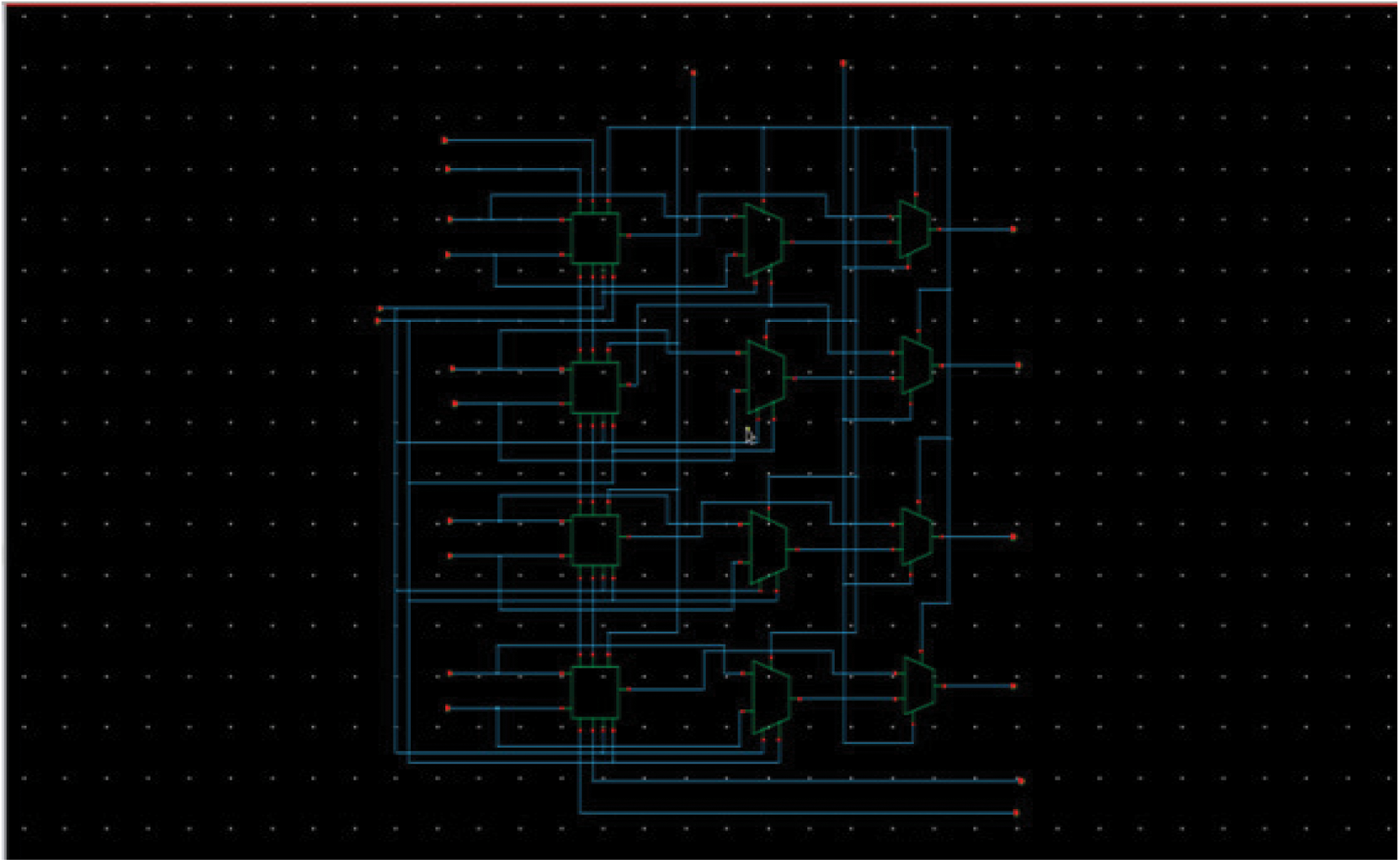
Figure 11: Design of 4 bit ALU with diode-connected sleep transistor
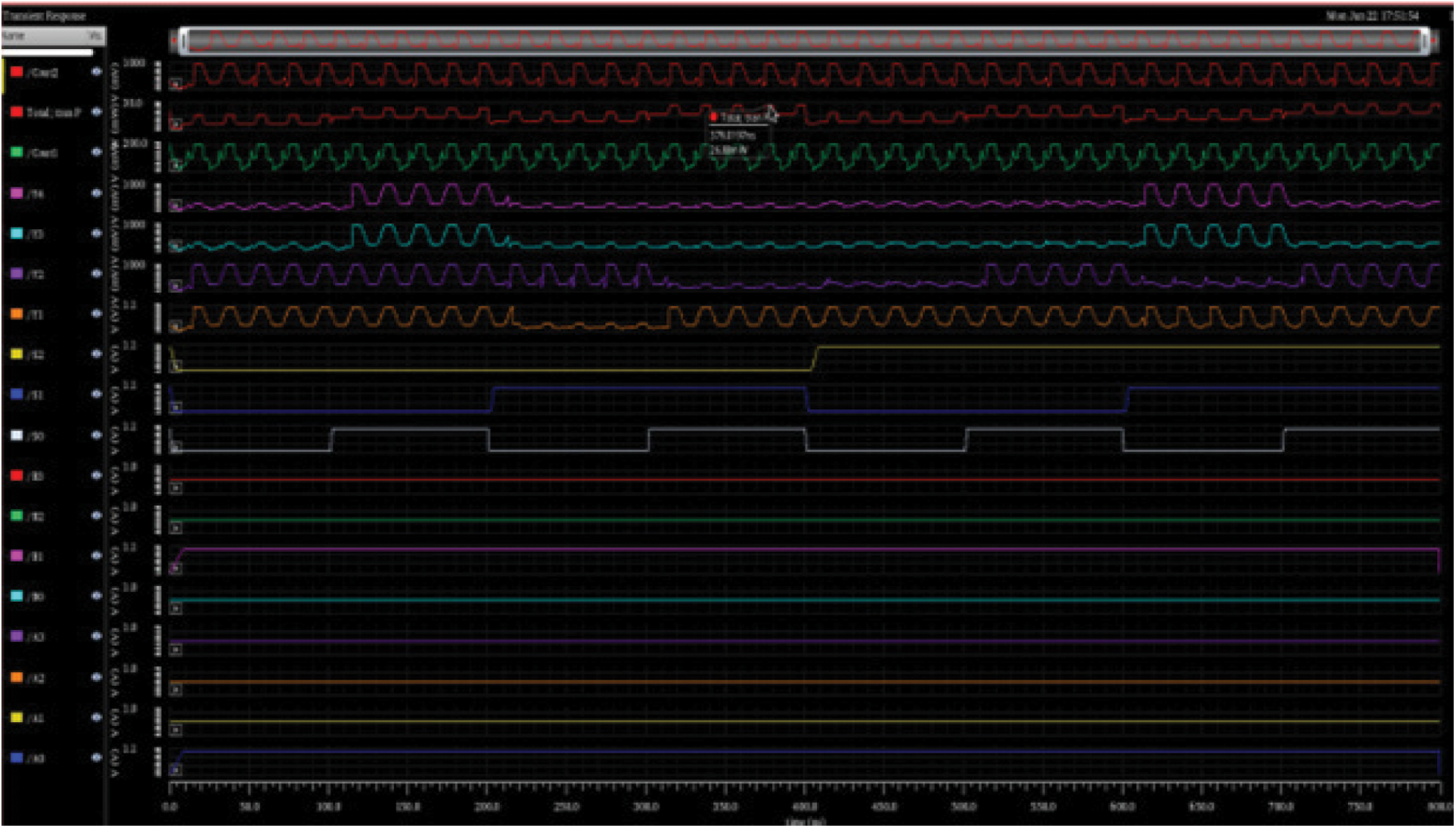
Figure 12: Simulation results of 4 bit ALU with diode-connected sleep transistor
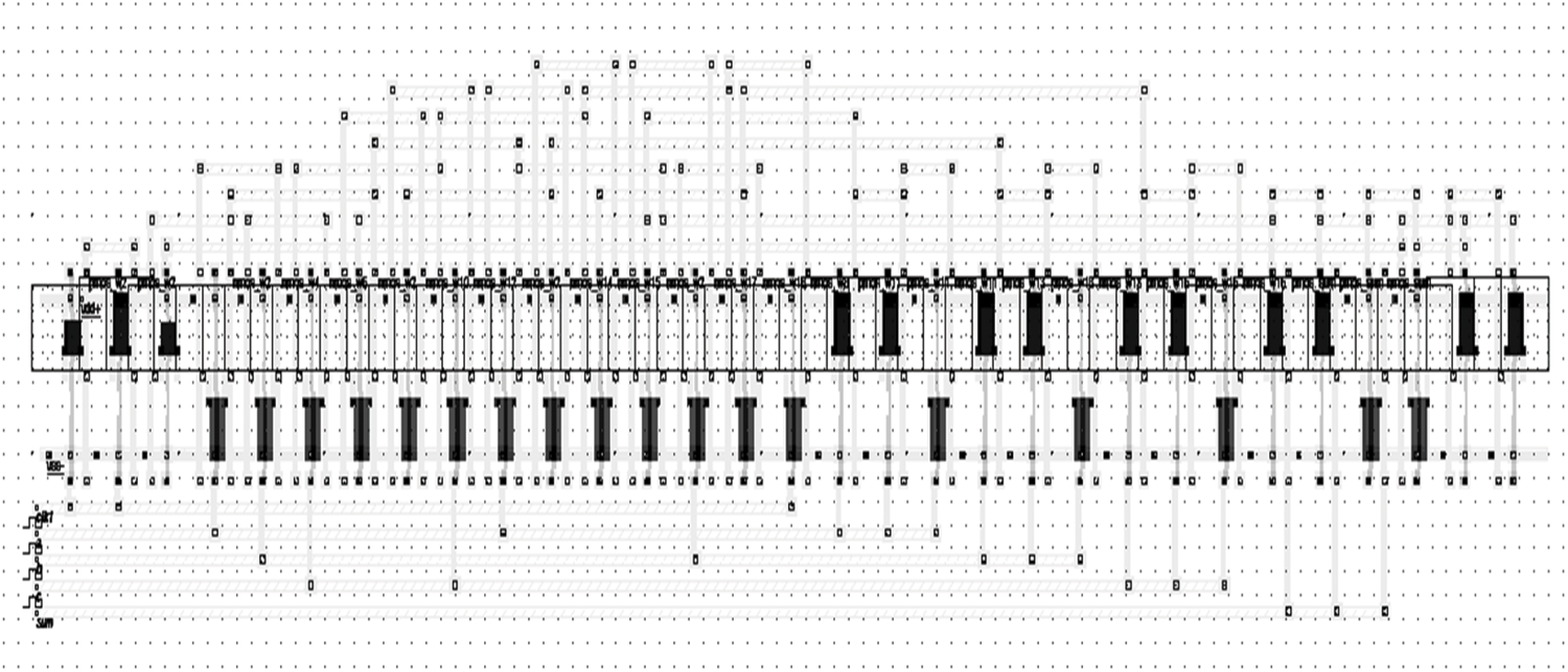
Figure 13: Layout of full adder using diode-connected sleep transistor
This paper proposes a 4-bit ALU framework using FinFET at 22 nm technology. To achieve power minimization, the Diode-connected sleep transistor module is connected to the actual logical circuits, including AND, OR, and Full adder. In the proposed design, nearly eight logical operations are performed with similar operation speed exhibited by the traditional CMOS technology. In the power minimization analysis, the independent gate mode is superior to the other three FinFET technology modes. The average consolidation of leakage power and leakage current of the SG, LP, and Hybrid modes is simulated, seen as 28.64 nW and leakage current as 135.24 pA, respectively. The proposed method is implemented in the independent mode for overcoming this leakage issue. The simulation result of independent gate mode 4-bit ALU using diode-connected sleep transistor is simulated, and leakage power is seen as 6.15 nW and leakage current as 42.85 pA. Leakage power obtained mainly depends on the input vector and applying Diode connected sleep transistor. It effectively reduces leakage power compared to CMOS (45 nm) and FinFET (22 nm) without a sleep transistor. The power-delay-product (PDP) for dynamic and static power where the proposed 4-bit ALU with Diode connected sleep transistor is much better for static power but a smaller power variation in dynamic due to addition of transistor in this model.
Funding Statement: The authors received no specific funding for this study.
Conflicts of Interests: The authors declare they have no conflicts of interest to report regarding this study.
1. S. Dwivedi and N. R. Prakash, “A study on recent advancements in VLSI technology using FinFETs,” International Journal of Innovative Research in Science, Engineering and Technology, vol. 4, no. 12, pp. 12789–12793, 2015. [Google Scholar]
2. S. R. Sanjana, S. Balaji Ramakrishna, Samiksha, R. Banu and P. Shubham, “Design and performance analysis of 6T SRAM cell in 22 nm CMOS and FINFET technology nodes,” in 2017 Int. Conf. on Recent Advances in Electronics and Communication Technology, Bangalore, India, pp. 38–42, 2017. [Google Scholar]
3. R. Singh and S. Jain, “Efficient deblocking filter with SRAM using 22 nm FinFET technology,” in 2021 Int. Conf. on Artificial Intelligence and Smart Systems, vol. 2, pp. 1470–1473, 2021. [Google Scholar]
4. D. Lakshmaiah, M. V. Subramanyam and K. S. Prasad, “Design of high speed low-power 1-Bit CMOS ALU,” International Journal of Technology and Engineering Science, vol. 2, no. 9, pp. 2284–2287, 2014. [Google Scholar]
5. M. Shrivastava, M. S. Baghini, D. K. Sharma and V. R. Rao, “A novel bottom spacer FinFET structure for improved short-channel, power-delay, and thermal performance,” IEEE Transactions on Electron Devices, vol. 57, no. 6, pp. 1287–1294, 2010. [Google Scholar]
6. S. A. Tawfik and V. Kursun, “Low-power and compact sequential circuits with independent gate FinFETs,” IEEE Transaction Computer Aided Design, vol. 26, no. 55, pp. 60–70, 2008. [Google Scholar]
7. A. Datta, A. Goel, R. T. Cakichi, H. Mahmoodi, D. Lakshmanan et al., “Modeling and circuit synthesis for independently controlled double gate FinFET devices,” IEEE Transaction Computer Aided Design, vol. 26, no. 11, pp. 1957–1966, 2007. [Google Scholar]
8. S. Chopra and S. Subramaniam, “A review on challenges for MOSFET scaling,” IJISET International Journal of Innovative Science, Engineering & Technology, vol. 2, no. 4, pp. 1–6, 2015. [Google Scholar]
9. J. Kanungo and S. Dasgupta, “Performance analysis of a complete adiabatic logic system driven by the proposed power clock generator,” IOPscience, vol. 35, no. 9, pp. 1–8, 2014. [Google Scholar]
10. M. Manasa, B. Shankar, J. Praveen and R. Raghavendra, “Design and implementation of ALU using FINFETs,” International Journal of Innovative Research in Electrical, Electronics, Instrumentation and Control Engineering, vol. 4, no. 5, pp. 8–16, 2016. [Google Scholar]
11. J. Jency and B. Lincy, “Design of low power 4 bit ALU using 32 nm FinFET technology,” International Journal of Pure and Applied Mathematics, vol. 120, no. 6, pp. 8089–8100, 2018. [Google Scholar]
12. W. Shin, S. Callender, S. Pellerano and C. Hull, “A compact 75 GHz LNA with 20 dB gain and 4 dB noise figure in 22 nm FinFET CMOS technology,” in 2018 IEEE Radio Frequency Integrated Circuits Symp., Philadelphia, PA, USA, pp. 284–287, 2018. [Google Scholar]
13. P. Suresh, K. Aanandhasaravanan, C. Iwendi, E. Ibeke and G. Srivastava, “An artificial intelligence-based quorum system for the improvement of the lifespan of sensor networks,” IEEE Sensors Journal, vol. 21, no. 15, pp. 1–13, 2021. [Google Scholar]
14. S. Markkandan, S. Sivasubramanian, J. Mulerikkal, N. Shaik, B. Jackson et al., “Massive MIMO codebook design using gaussian mixture model based clustering,” Intelligent Automation & Soft Computing, vol. 32, no. 1, pp. 361–375, 2022. [Google Scholar]
 | This work is licensed under a Creative Commons Attribution 4.0 International License, which permits unrestricted use, distribution, and reproduction in any medium, provided the original work is properly cited. |