DOI:10.32604/iasc.2023.028758
| Intelligent Automation & Soft Computing DOI:10.32604/iasc.2023.028758 | |
| Article |
Adaptive Sub-Threshold Voltage Level Control for Voltage Deviate-Domino Circuits
1Department of Electronics and Communication Engineering, Mahendra Engineering College, Namakkal, 637503, India
2Department of Electrical and Electronics Engineering, KSR College of Engineering, Tiruchengode, 637215, India
*Corresponding Author: C. Arun Prasath. Email: arunprasathc2004@gmail.com
Received: 16 February 2022; Accepted: 29 March 2022
Abstract: Leakage power and propagation delay are two significant issues found in sub-micron technology-based Complementary Metal-Oxide-Semiconductor (CMOS)-based Very Large-Scale Integration (VLSI) circuit designs. Positive Channel Metal Oxide Semiconductor (PMOS) has been replaced by Negative Channel Metal Oxide Semiconductor (NMOS) in recent years, with low dimension-switching changes in order to shape the mirror of voltage comparator. NMOS is used to reduce stacking leakage as well as total exchange. Domino Logic Circuit is a powerful and versatile digital programmer that gained popularity in recent years. In this study regarding Adaptive Sub Threshold Voltage Level Control Problem, the researchers intend to solve the contention issues, reduce power dissipation, and increase the noise immunity by proposing Adaptive Sub Threshold Voltage Level Control (ASVLC)-based domino circuit. The efficiency and effectiveness of the domino circuit are demonstrated through simulation results. The suggested system makes use of high-speed broad fan-gate circuits, occupies minimum space, and consumes meagre amount of power. The proposed circuit was validated in Cadence simulation tool at a supply voltage of 1V, frequency of 100 MHz, and an operating temperature of 27°C with 64 input OR gates. As per the simulation results, the suggested Domino Gate reduced the power dissipation by 17.58 percent and improved the noise immunity by 1.21 times in comparison with standard domino logic circuits.
Keywords: Domino logic; power consumption; figure of merit; adaptive sub-threshold voltage level; wide fan-in gates
Jhamb Mansi et al. 2016 proposed dynamic logic gates for wide fan in gates as a discretionary decision for expansive memory and rapid applications. This is because it is located near standard Complementary Metal-Oxide-Semiconductor (CMOS) logical gates [1]. Domino logic circuits can achieve high speed, thanks to its low noise edge compared to standard CMOS logic. Likewise, low noise mark demonstrates the expanded affectability in domino logic circuit to ensure the noise immunity increases. Domino logic circuits gets upgraded by noise insusceptibility which, on the other hand, downscales the innovation. This circuit is prevalently utilized in vital applications. At this point, the supply voltage is estimated to reduce the utilization of power due to which the delay increases in this circle. Therefore, primary voltage change is supplied in conjunction with voltage scaling in order to compensate the delay discussed above. When there is a reduction in primary voltage, domino logic circuit speed increases. However, based on the response of sub-threshold leakage, the noise immunity response gets changed, as per the literature, Vijay Kumar Sharma et al. 2021, Hathwalia Shruti et al. 2021 [2,3].
The thickness of the gate oxide reduces the scaling technology since the leakage technique increases the scaling of technology transformation. This leakage is presented to current domino circuit. Hence, the productivity of domino logic circuit remains low in high voltage leakage streams and noise sources which has low threshold. During leakage of the transistor, the limit increases quickly. At the time of expansion, the leakage gets reduced to current noise soundness and decreases the Domino circuit to have more information noise. Noise invulnerability is one of the key tests used for domino OR gate framework. Pull Down Network (PDN) is a parallel blend of transistors in domino OR gate structure. The extension network might get leaked effectively from the hub to change from the assessment stage, when the remuneration clock is higher. Domino OR gates in wide fans get questioned, whereas the dynamic nodes results in the failure of logic circuit. In order to deal with the problem of charged leaking, a weak P-channel Metal–Oxide–Semiconductor (PMOS) keeper transistor M2 is used to protect the node as shown in Fig. 1. In gatekeeper mode, the transistor M2 improves noise insusceptibility and decreases the load leakage in dynamic node.
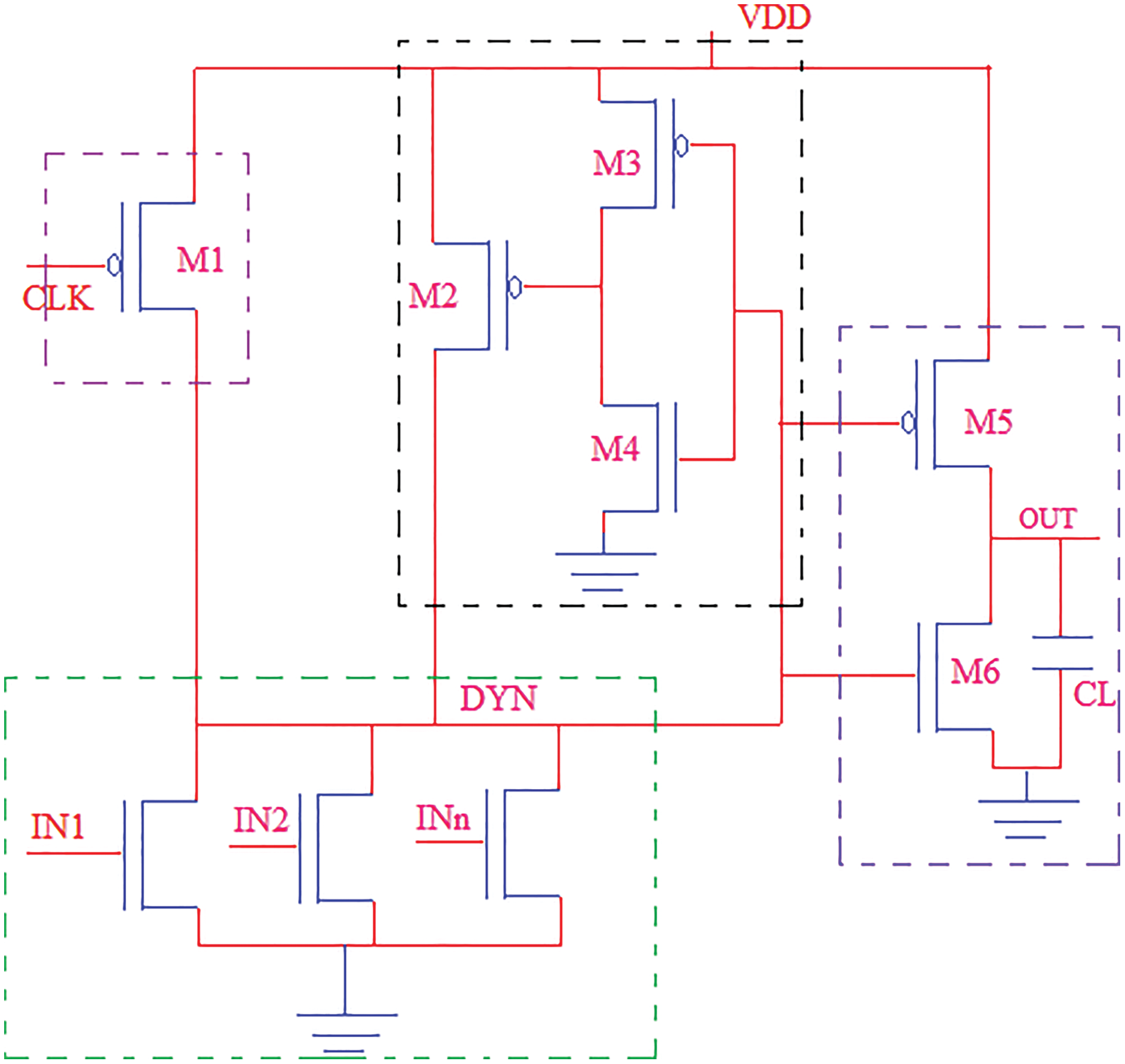
Figure 1: Standard footless domino circuit
Eq. (1), given below, is used to evaluate the average power consumption of domino logic gates.
where
Pavg = Average Power consumption,
Pshort = short Circuit power consumption,
Pswitch = Power consumption in load capacitance
Pleakage = Power consumption against sub-threshold leakage and gate switching current.
When the power utilization of different parts gets reduced, gadget measurements and supply voltage too get reduced. Koshy et al. 2015 mentioned that the current leakage increases in case of unnecessary Short Channel Effects (SCEs). Bhanu Chandr et al. 2013 [4,5] discussed about the causes behind the scaling of devices. These short-channel effects, in turn, reduce the device’s threshold and the length of the channel effectively. Domino’s logic circuits have been proposed in literature to reduce power consumption. These technologies have been developed using basic Foot Domino Logic (FDL) and Footless Domino Logic (FLDL), Rajesh Kumar Paul et al. 2018, M. Hanumanthu et al. 2016 [6,7]. In these studies, it has been proposed that additional P and N transistors can be used to reduce energy consumption and delay the press coverage and domino circuits to improve the immune system.
The current paper discusses about Adaptive Sub Threshold Voltage Level Control Problem in which the researchers addresses the contention issues and aim to reduce power dissipation, and increase noise immunity. Both efficiency and effectiveness of domino circuit are demonstrated through simulation results. The suggested system uses high-speed broad fan-gate circuits, occupies a minimal amount of space and consumes meagre amount of power. The Suggested Adaptive Sub Threshold Voltage Level Control (ASVLC)-based domino circuit was validated using Cadence simulation tool with a supply voltage of 1 V, a frequency of 100 MHz, and an operating temperature of 27°C with 64 input OR gates.
Rest of the paper is organized as follows. Section 2 examines the conventional Domino Circuits and the challenges associated with it. The proposed power leakage control-based Domino logic operations are discussed in Section 3. Simulation results and performance analysis are given in Section 4. Section 5 concludes the paper and provides future enhancement of the entire work.
In recent years, wide fan-in domino has been broadly utilized for elite microprocessors and VLSI circuits. The fan-in domino logic requires a little PMOS keeper to maintain the vast dynamic tip stability. However, if domino logic number is large in size, then a large PMOS keeper is inevitable according to Deepika Bansal et al. 2017 [8]. In the meantime, the threshold range should be reduced to meet the proficiency requirements. As a result, the rapid growth of current threshold increases with the development of low-threshold technology, Nikhil Saxena et al. 2013 [9]. Domino’s logic design techniques are proposed to achieve less consumption of active power, C. J. Akl et al. 2008, Parham Hosseinzadeh Namin et al. 2018 [10,11]. Due to the current conflict between PMOS keeper and expansion logic under N-channel Metal-Oxide Semiconductor (NMOS), the delay-time control scheme got delayed at the beginning of evaluation. Therefore, a large keeper can be implemented without a significant reduction in performance and wastage of power.
Likewise, noise margin is an appropriate field according to Priydarshi et al. 2016 [12] because domino logic has achieved much benefits after validity. The keeper control of clock region and the power of control circuit in Domino Logic are still observed with insignificant leakage, Peiravi et al. 2009, Shah et al. 2016 [13,14] and are adjusted because of the inner dynamic hub delay. This in turn reduces the leak power of both dynamic and sleep mode. If all the information inputs are low, the dynamic middle hub voltage begins for rest mode, Rajeev Kumar et al. 2014, Uday [15]. This yield, according to Panwar et al. 2013 [16], prompts the inverter to disseminate short-circuit power. Aside from this, another method of Split Domino (SD) circuit was proposed by Ankit Kori et al. 2015 [17]. In this circuit, PDN protector transistors and standard footless domino circuit are isolated into two equivalent parts.
Furthermore, Kuldeep Patel et al. 2016 [18] proposed a type of domino circuit called saturated keeper domino circuit. In comparison with normal transistor, the source transistor is connected to the output of the inverter in saturated keeper method F. Frustaci et al. 2009 [19]. If such an arrangement is modified, the power consumption pattern of the lower network gets reduced. This Domino pattern helps in improving the circuit speed. In addition, a strong controlling keeper domino logic circuit is another technique that can boost immunity according to Volkan Kursun et al. 2003 and T. Gupta et al. 2013 [20,21]. A simple CMOS domino controls the strongest keeper transistor. All inputs of this circuit are low voltage whereas CMOS output releases the controlling circuits, Li Ding et al. 2004 [22]. Therefore, solid keeper transistors should be increased in order to decrease the leakage. This circuit has an advantage i.e., high voltage and with this capacity, CMOS circuit yield is high which significantly increases the Domino’s circuit speed.
Furthermore, Leakage Current Replica (LCR), as per the studies conducted earlier such as Mohammad Asya et al. 2018, Yolin Lih et al. 2007 [23,24] PDN Massimo Alioto et al. 2010 [25] controls the current leak proposition of the proposed keeper circuit. When the circuit is processed, it changes the current, voltage, and temperature analog current in mirror. By using an analog current mirror in this region, the standard deviation reduces the current as well as the process of switching it to PDN, Michele De Marchi et al. 2014 [26]. The current clock is delayed by a domino circuit in sleep state mode according to Romain Ritzenthaler et al. 2016 [27]. This circuit clock delay is an odd number of inverter chains. By delaying the clock motion at this rating, if the data sources are high, the current PDN diminishes, as per literature, Ali Peiravi et al. 2013, Shilpa Kamde et al. 2014, Pratosh Kumar Pal et al. 2016, K. Sangeetha et al. 2016 [28–31].
In all of the preceding techniques, the framework is determined to have a cascade connection issue. This results in some consequences including the degradation of circuit performance in terms of area, power dissipation, and latency. As a result, a new actuated methodology is proposed in this study to address the difficulties.
Fig. 2 illustrates the block diagram of the suggested voltage deviate-domino logic. Pre-charge assessment and voltage deviate-domino logic circuit are two major building blocks in this set up. Domino gate design is a high-voltage comparator with low output voltage, based on full voltage differential across the pull-down network. It is used to handle this operation. Voltage comparator is designed to replace the PMOS with NMOS for low-level switching and for designing the mirror voltage comparator. Furthermore, stacking leakage and cascade style of NMOS are carried out to reduce the overall current switching.
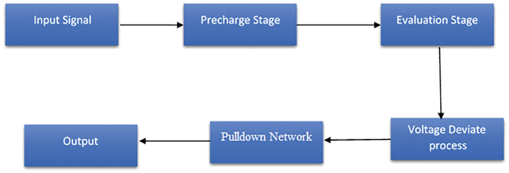
Figure 2: Block diagram of voltage deviate-domino circuit
3.1 Proposed Adaptive Sub Threshold Voltage Level Controlled Domino Circuit
The functional circuit diagram of the proposed domino is depicted in Fig. 3. Low process variations and power dissipation of wide fan-in are designed using the Proposed Adaptive Sub Threshold Voltage Level controller. These wide fan gates contain two stages such as Voltage Comparator and Domino Gate. With the help of wide-OR logic, the two voltage nodes A & B have been implemented. In the first stage, A and B produce voltages which are charged at Dynamic Node (DN) and final output from the second stage. In case of leakage in current, mirror is incorporated into DN for repeated charges. This is done so by replacing a branch with another branch. Both charging and discharging the terminal is highly useful, because the output is efficiently controlled. Thus, the noise gets changed and the output has a high impact on the node. As a result, the DN effectively increases the gate and the process variations decrease the effect. Thus, the noise turns into a large impact between output nodes. Consequently, the DN in the node increases and reduces the effect of the procedural differences.
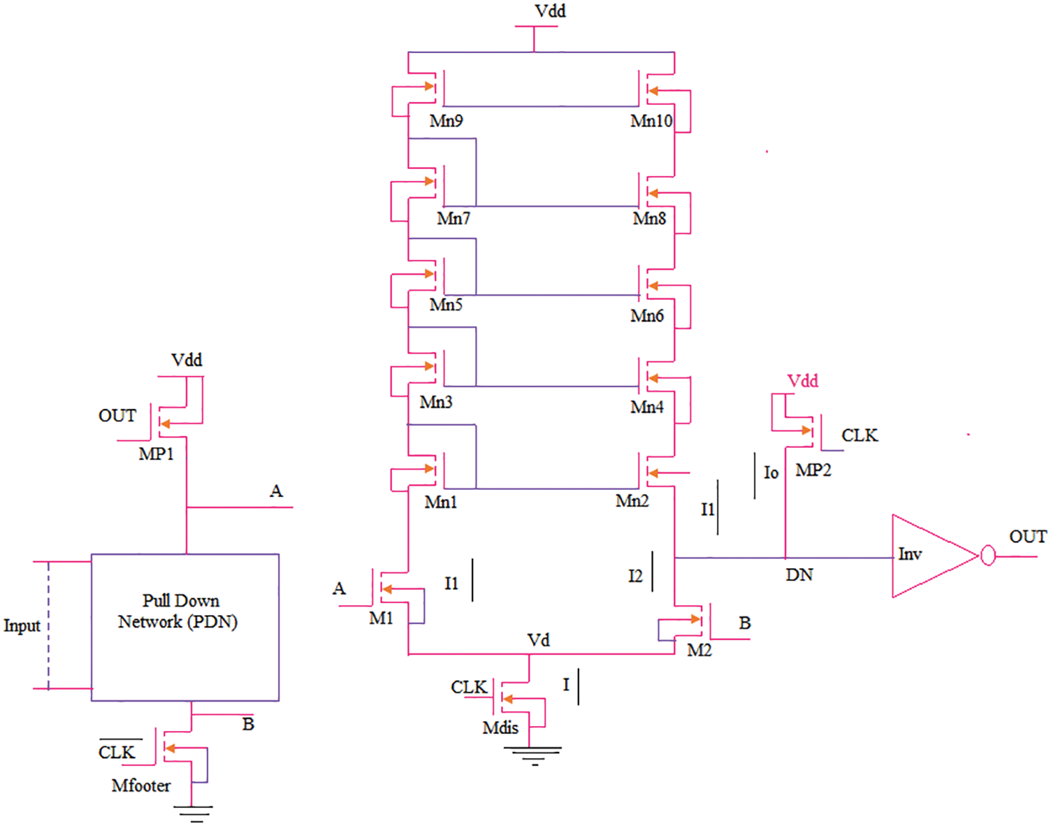
Figure 3: The proposed domino circuit
This design is developed to be used with NMOS as a mirror. When compared with NMOS, numerous advantages are present in this method. NMOS increases the current consumption in response to high mobility response. The present mirror is used to duplicate another arm. Channel Length Modulation (CLM) cannot be altered due to the current in simple mirror. The order is removed in a cascade current mirror to get rid of CLM effect. As the transistor sticks in the mirror, the NMOS threshold range gets automatically increased. In response to PDN reduction, the leak current gets significantly reduced. Pre-designed models mention that some of the charges may directly damage the PDN into current, number of stages, and the transistor size of PDN. In first phase, the Mfooter transistor size should be much higher than EP which is similar to MDIS transistor in the second stage of leakage current. As DN gets discharged by M2, the right-hand trail must be higher than the other hand of VC operations. The rate of the mirror is evaluated using Eq. (2).
Likewise, the quantity of transistors in mirror proportion decreases the stacking which in turn reduces the NI as well. Therefore, mirror ratio that comes with the size of all-transistor mirror is higher. While the area can be lesser, it is less likely to be so. M1 should be controlled by M2 node because it ultimately results in being controlled at voltage B. There are two active phases similar to the standard dynamic gate in this circuit design. The design is described through two stages such as Precharge Phase and Evaluation Phase.
The precharge structure round map is shown in Fig. 4. In this precharge stage, Mdis is turned into OFF stage, whereas PDN transistors are also turned off. Meanwhile, transistors Mfooter and MP2 are turned into ON state. Hence the DN acts as an inverter which makes the OUT low and transistor mp1 ON. Further, the receiver that starts to charge the node gets out due to a cut out in the inverter. If the load actions of node A is under threshold leakage, the Mfooter transistor is turned into ON stage so as to maintain zero voltage at node B. In this case, no ‘1’ logic node will be available from VDD for ‘1’ argument through M2 transistor i.e., it gets loaded from the ground in the direction of DN and ground due to the node, VDD.
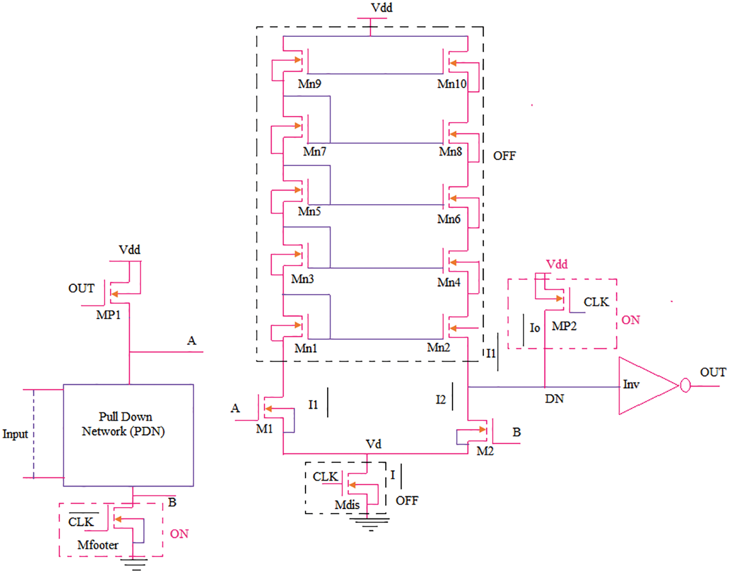
Figure 4: Precharge phase
The evaluation phase circuit diagram is depicted in Fig. 5. At the time of evaluation, CLK is turned into either ON or OFF stage while MP2, and Mfooter maintain the Backstage Voltage.
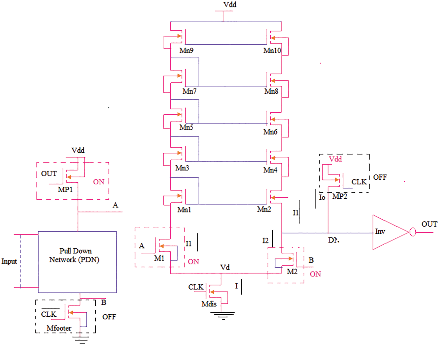
Figure 5: Evaluation phase
Since the rating build transistor Mp1 remains the prerequisite for initialization, it may be turned OFF or ON based on the response of input. At present, NMOS transistors are associated with PDN due to which the activity comes down. PDN transistor contributions can be all high or all low, while at times, some high and low contentions can be loose. At present, both circumstances can be considered. The node has the least logic which means the PDN with all inputs indicate that high voltage is the first one among all transistors in cut-off mode. This voltage gets distributed to the current edge B in sub-threshold, due to a small fraction. As a result, M2 transistor can be switched using this low voltage. Therefore, DN remains at high logic, whereas low logic is found in the position on transistor Mp1 out. At present, no less than one input must be of higher logic, while the second position begins with NMOS in PDN. Therefore, both transistors M1 and M2 have been turned into ON state and the ground begins to reduce M2 and MDIS, as the conduction path between DN and ground gets reduced.
I1, I2 and I0 flow through the currents, M1, M2, and MP2 transistors respectively. As shown in Fig. 3. Let DN have internal capacitances such as Cdyn and Cload and copy the current I1 to other branch. This section discusses the works of all the transistors. As defined earlier, voltages A and B are placed across the PDN. In this section, the discharge of charging and Cdyn are discussed.
In precharge phase CLK = 0 V, the transistor MP2 is turned ON as it is charged through Cdyn MP2. This starts NMOS transistors of INV on the outside node. As the MDIS is closed, the current (I) flows through and then, I1 and I2 becomes equal to zero.
where
I0 = current consumption of Mp2 t. In evaluation phase, the clock = 1 V and transistor MP2 are turned OFF i.e., I0 = 0. During the evaluation phase, an existing transistor on MDIS flows through the transistor. The following conditions can be applied herewith.
Case 1: When node A = 1 V and B = 0, the M2 transistor is turned OFF and M1 is turned ON. If any charge leakage is caused by Isub based on the response of the M2 transistor, then the following equation applies.
Case 2: If A = 1 V and B = 1V. Due to I2 (W / L), more than I1 is 2 (W / L) greater than 1. Thus, the discharge of Cdyn starts on the outside node and the PMOS transistor of INV starts on the Cload
3.3 Estimation of Noise Immunity, Power Consumption and Figure of Merit
3.3.1 Estimation of Power Utilization
To reduce power consumption, voltage-deviate domino circuits should be incorporated in all the active components in a specified voltage-deviate landslide circuits. The dynamic gate pulses include power dissipation, short circuit power, and flipping strength. The following equation represents the average power of an electric gate (6).
where
The switching Power Range (PS) exists as a result of charging and discharging of circuit tech capabilities. It may be calculated using the Eq. (6), which is proportional to voltage swing.
VDD denotes the maximum voltage oscillation in traditional domino circuits, while it is equal to the voltage between VDD and VS. Consequently, the following equation is used.
Many metrics have been defined in the literature to compare noise immunity. UNG (Unity Noise Gain) range is commonly used in the evaluation of noise immunity metric which is incorporated herewith using the following Eq. (8). (UNG).
The main flaw of UNG is that the duration ranges of output pulses are not taken into account. To circumvent this constraint, the proposed work calculates the Unity Noise Average (UNA) value, which considers the duration ranges of output pulses. It is calculated using the following Eq (10).
When compared to UNA in domino circuits, the voltage level in input noise is adjusted to an average noise level than the input noise range. The same noise is used in the assessment phase in worst-case scenario of measuring strength, when all the input gates are used.
At the time of comparing circuits, the following Figure of Merit (FOM) is used to compare energy consumption, delay, noise, and immunity.
where
All the settings of broad input OR gates are conventional circuit specifications. The voltage swing of dynamic node is limited to a voltage-deviate domino circuit. But noise immunity becomes increasingly important during the evaluation phase for following reasons. When under-expanded network is on any transmission path, any unwanted voltage drop on the transistor compensates the dynamic node. The voltage difference between the feet is thus extinguished in this situation, due to increasing voltage of the transistor in the node. The output voltage remains unchanged, because the transistor is smaller than the voltage of the target.
4 Simulation Results and Discussions
The proposed domino logic was created using Adaptive Sub Threshold Voltage Control method. The simulation parameters for the recommended voltage deviate domino logic circuit are shown in Tab. 1. Maximum power reduction, in Domino Logic Gate with adaptive sub-threshold voltage control mechanism, was achieved at 90 nm compared with 8 to 256 bit wide fan spice simulation of 0.8 V.
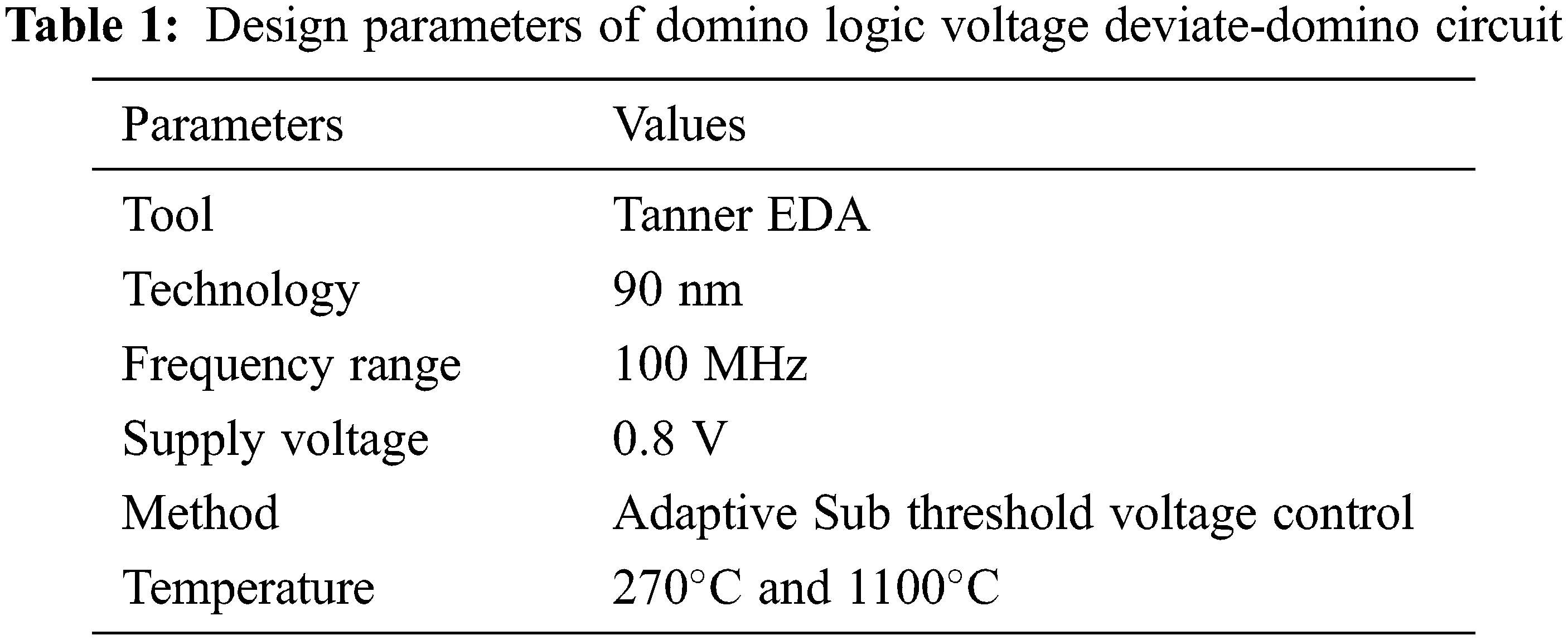
Fig. 6 shows the transient response simulation results of the proposed Domino Logic. In the following figure and table, the performance analysis result is tabulated for power and unity noise average.
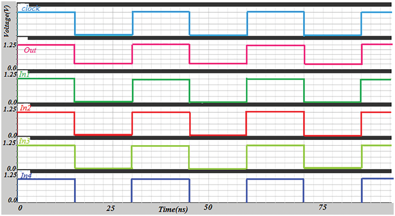
Figure 6: Transient response of proposed domino
Tab. 2, Figs. 7 and 8 compare the unity noise average and adjusted unity noise average reduction performance compared to existing domino logic circuits based on Current Comparison Domino (CCD), Voltage Comparison Domino (VCD) and Prescient Innovation Model (PIM) techniques. The proposed ASVLC-based voltage deviation domino logic delivered the best results against all Fan-in bits. In 64-bit, the normalized UNA of CCD was 1.86, VCD was 2.31, PIM was 2.62, and ASLV was only 2.79.
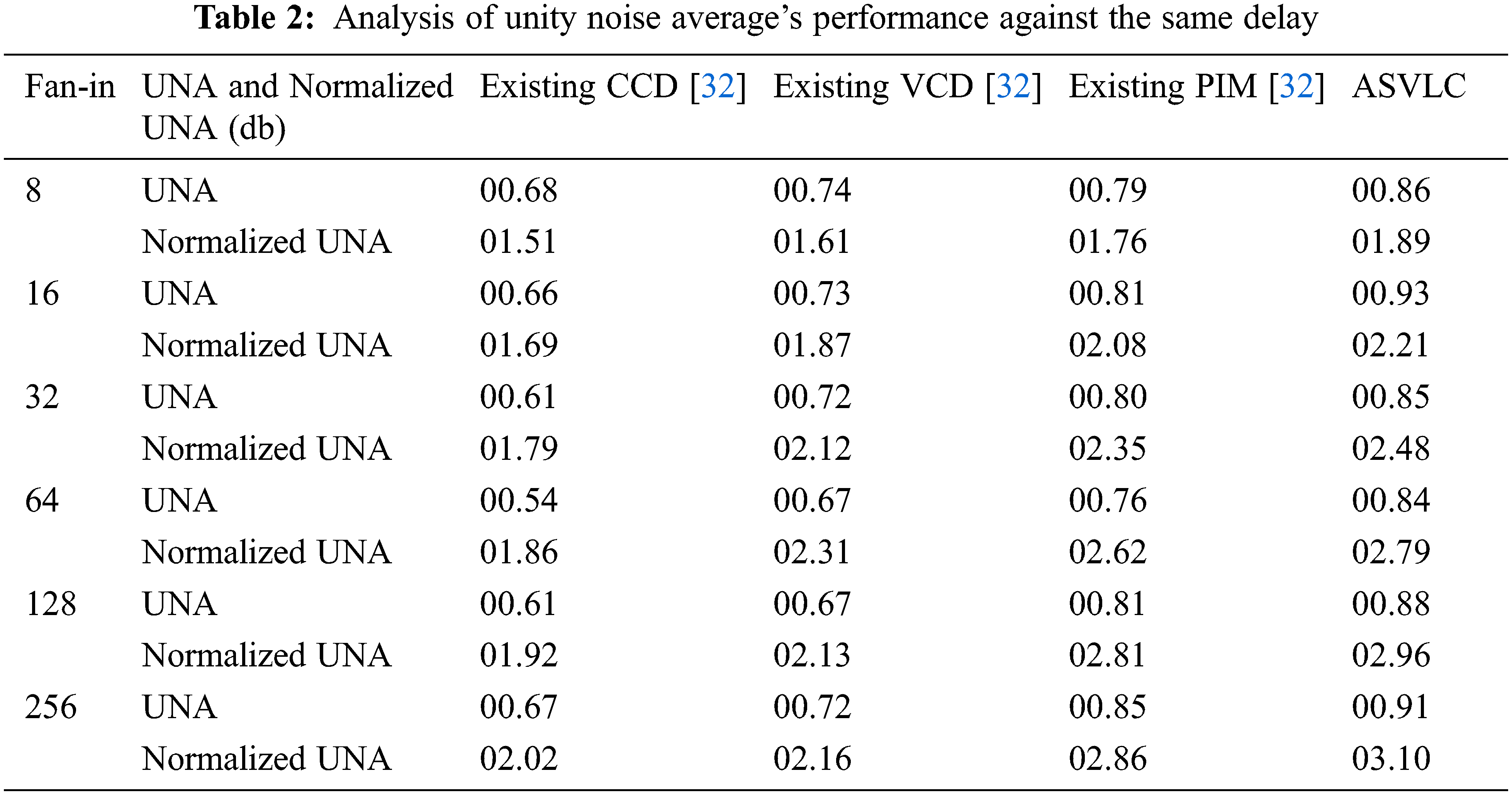
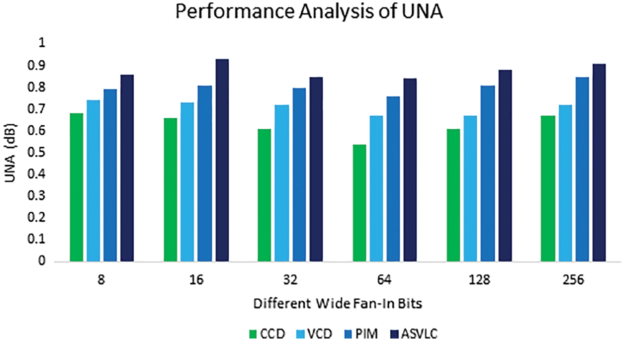
Figure 7: Performance analysis of UNA
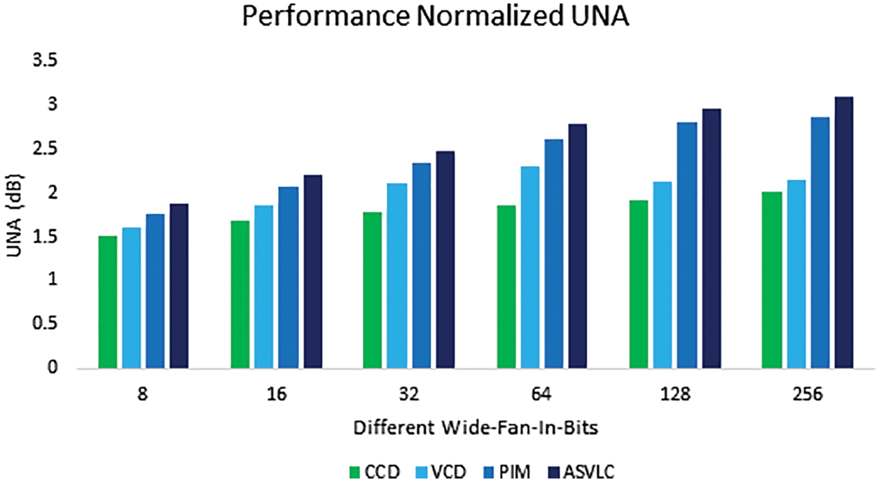
Figure 8: Performance analysis of normalized UNA
Tab. 3, Figs. 9 and 10 compare the consumption of power and normalized power. When compared to existing CCD, VCD, and PIM-based domino logic circuits, the suggested ASVLC-based voltage deviation domino logic circuit achieved the best results against all Fan-in bits For instance, in 64-Bit, CCD had a normalized power of 0.66, VCD had a normalized power of 0.65, PIM had a normalized power of 0.57, and ASVLC had a normalized power of 0.51.
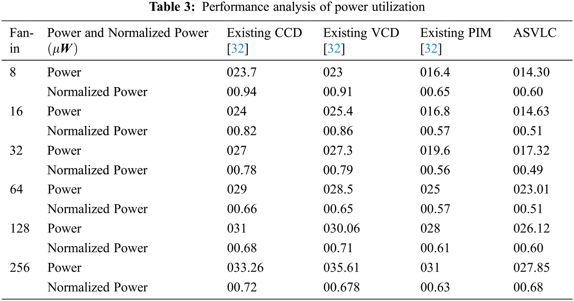
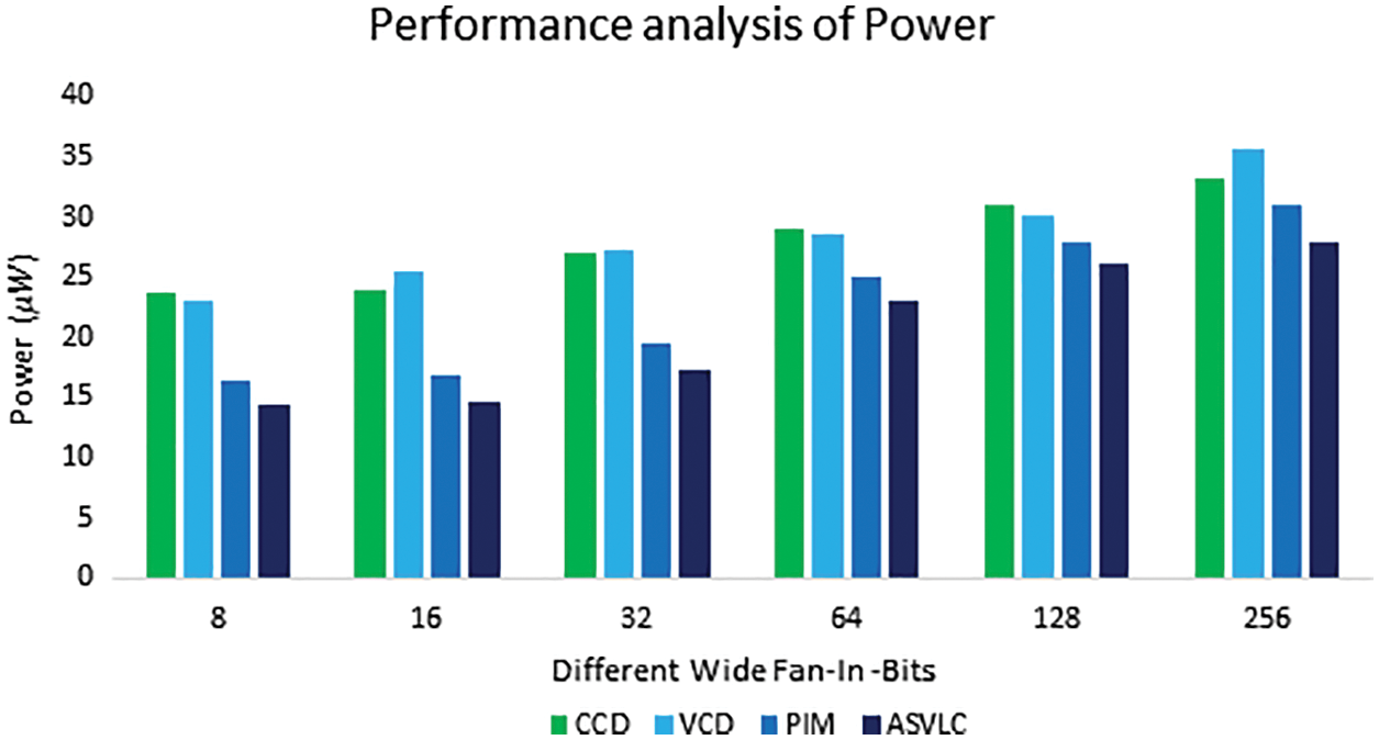
Figure 9: Performance analysis of power
Figure 10: Performance analysis- normalized power
Fig. 11 shows the results of FOM performance that discusses about the performance of a company. Because, the pull-down network power usage is decoupled and the proposed ASVLC-based voltage-deviated domino circuits outperform conventional CCD, VCD, and PIM-based domino circuits across all parameters.
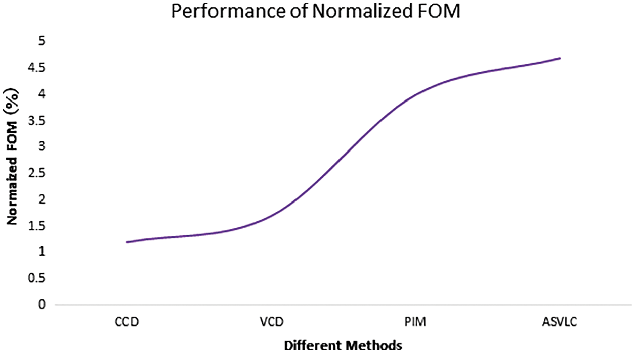
Figure 11: Performance analysis for Fig. of Merit in 16-input OR gate with different methods
Fig. 12 shows the results of ASVLC-based voltage-deviated domino circuits compared against existing CCD, VCD, and PIM-based domino circuits in terms of time delay performance. As previously stated, the suggested PIM-based voltage-deviate domino circuit technique was tested under different parameters and the method produced perfect results across all the metrics.
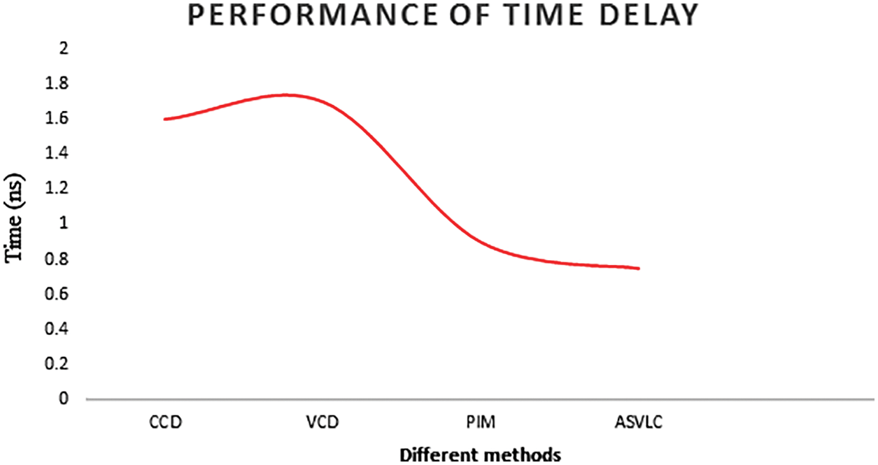
Figure 12: Comparison of the time delay
In this study, a new technique has been proposed based on domino circuits to overcome the present issues. Based on the simulation results, it has been found that the recommended domino logic circuit has numerous advantages including low power consumption and short propagation latency. Before delivering an output, the recommended adaptive sub-threshold voltage level control-based domino system compares the voltages throughout the pull-down network. As a result, the performance gets improved, while resilience is preserved. The pull-down network is separated from the suggested ASVLC inverter by a voltage swing in downward network and the propagation delay is done to reduce power consumption of the gates. The switching voltage threshold of the suggested domino circuit was found to be nearly twice that of the threshold range of NMOS transistors. As a result, the overall performance of the proposed system got improved, particularly the number of fan-ins. For example, the 64-bit fan in CCD had a normalized power of 0.66, VCD had a normalized power of 0.65, PIM had a normalized power of 0.57, and ASVLC had a normalized power of 0.51. In future, the proposed model can be incorporated in real-time environment as well.
Funding Statement: The authors received no specific funding for this study.
Conflicts of Interest: The authors declare that they have no conflicts of interest to report regarding the present study.
1. M. Jhamb and G. Singh, “Efficient adders for assistive devices,” Engineering Science and Technology International Journal, vol. 20, no. 1, pp. 95–104, 2016. [Google Scholar]
2. S. Vijay Kumar, “A survey of leakage reduction techniques in CMOS digital circuits for nanoscale regime,” Australian Journal of Electrical and Electronics Engineering, vol. 18, no. 4, pp. 217–236, 2021. [Google Scholar]
3. H. Shruti and G. Naresh, “A review of leakage power reduction techniques for VLSI applications,” International Journal of Electronics and Communication Engineering, vol. 4, no. 12, pp. 312–324, 2021. [Google Scholar]
4. L. Koshy and G. Chandran, “Low leakage and high performance tag comparator implemented in 180 nm CMOS technology,” Procedia Computer Science, vol. 1, no. 46, pp. 1261–1267, 2015. [Google Scholar]
5. D. B. Chandra, “Suppression of short channel effects (SCES) by dual material gate vertical surrounding gate (DMGVSG) MOSFET: 3-D TCAD simulation,” Procedia Engineering, vol. 64, no. 2, pp. 125–132, 2013. [Google Scholar]
6. P. R. Kumar, “Analysis of various domino logic designs for low power consumption noise immunity and high-speed performance,” International Journal of Research Culture Society, vol. 2, no. 3, pp. 358–369, 2018. [Google Scholar]
7. M. Hanumanthu and N. B. Dastagiri, “Design and comparative analysis of domino logic styles,” Indian Journal of Science and Technology, vol. 9, no. 33, pp. 1–6, 2016. [Google Scholar]
8. D. Bansal, “Efficient keeper for pseudo domino logic,” International Journal of Pure and Applied Mathematics, vol. 117, no. 16, pp. 605–612, 2017. [Google Scholar]
9. N. Saxena, “Leakage current reduction in CMOS circuits using stacking effect,” International Journal of Application or Innovation in Engineering & Management, vol. 2, no. 11, pp. 985–997, 2013. [Google Scholar]
10. C. J. Akl and M. A. Bayoumi, “Single-phase SP-domino: A limited-switching dynamic circuit technique for low-power wide fan-in logic gates,” IEEE Transactions on Circuits and Systems, vol. 55, no. 2, pp. 141–145, 2008. [Google Scholar]
11. P. H. Namin, C. Roma, R. Muscedere and M. Ahmadi, “Efficient VLSI implementation of a sequential finite field multiplier using reordered normal basis in domino logic,” IEEE Transactions on Very Large Scale Integration (VLSI) Systems, vol. 26, no. 11, pp. 2542–2552, 2018. [Google Scholar]
12. L. Priydarshi and M. K. Chattopadhyay, “Low-power and high-speed technique for logic gates in 20 nm double-gate Fin FET technology,” Journal of Physics: Conference Series, America, vol. 755, no. 1, pp. 10255–10267, 2016. [Google Scholar]
13. F. Peiravi, S. Moradi and T. Dag Wisland, “Leakage tolerant, noise immune domino logic for circuit design in the ultra-deep submicron CMOS technology for high fan-in gates,” Journal of Applied Sciences, vol. 9, no. 2, pp. 392–396, 2009. [Google Scholar]
14. K. Shah, G. Ambika, M. Neema and L. Shreeniwas, “DOIND: A technique for leakage reduction in nanoscale domino logic circuits,” Journal of Semiconductors, vol. 37, no. 5, pp. 5501–5514, 2016. [Google Scholar]
15. S. R. Kumar and D. M. K. Singh, “Performance of low power domino circuits using pseudo-dynamic buffer,” IOSR Journal of VLSI and Signal Processing (IOSR-JVSP), vol. 4, no. 6, pp. 62–69, 2014. [Google Scholar]
16. U. Panwar, “Comparision on different domino logic design for high performance and leakage-tolerant wide or gate,” International Journal of Engineering Research and Applications, vol. 3, no. 6, pp. 2048–2052, 2013. [Google Scholar]
17. A. Kori, “Comparative analysis of domino logic circuits for better noise and delay performance,” International Journal of Engineering Trends and Technology (IJETT), vol. 30, no. 3, pp. 321–339, 2015. [Google Scholar]
18. K. Patel, “Leakage power reduction by using sleep switches in domino logic circuit design in DSM technology,” International Journal of Computer Applications, vol. 145, no. 7, pp. 876–882, 2016. [Google Scholar]
19. F. Frustaci, M. Lanuzza, P. Zicari and S. Perri, “Low-power split-path data-driven dynamic logic,” IET Circuits, Devices & Systems, vol. 3, no. 6, pp. 303–312, 2009. [Google Scholar]
20. V. Kursun, “Domino logic with variable threshold voltage keeper,” IEEE Transactions on Very Large Scale Integration (VLSI) Systems, vol. 11, no. 6, pp. 982–995, 2003. [Google Scholar]
21. T. Gupta and K. Khare, “A new technique for leakage reduction in 65 nm Footer less Domino Circuits,” Circuits and Systems, vol. 4, no. 2, pp. 209–216, 2013. [Google Scholar]
22. L. Ding and P. Mazumder, “On circuit techniques to improve noise immunity of CMOS dynamic logic,” IEEE Transactions on Very Large Scale Integration (VLSI) Systems, vol. 12, no. 9, pp. 910–925, 2004. [Google Scholar]
23. M. Asya, “A domino circuit technique for noise-immune high fan-in gates,” Journal of Circuits Systems and Computers, vol. 27, no. 10, pp. 347–358, 2018. [Google Scholar]
24. Y. Lih, N. Tzartzanis, W. William and W. Walker, “A leakage current replica keeper for dynamic circuits,” IEEE Journal of Solid-State Circuits, vol. 42, no. 1, pp. 48–55, 2007. [Google Scholar]
25. M. Alioto, G. Palumbo and M. Pennisi, “Understanding the effect of process variations on the delay of static and domino logic,” IEEE Transactions on Very Large Scale Integration (VLSI), vol. 18, no. 5, pp. 697–710, 2010. [Google Scholar]
26. M. D. Marchi, J. Zhang, S. Frache and D. Sacchetto, “Configurable logic gates using polarity-controlled silicon nanowire gate-all-around FETS,” IEEE Electron Device Letters, vol. 35, no. 8, pp. 880–882, 2014. [Google Scholar]
27. R. Ritzenthaler, “Diffusion and Gate Replacement: A new gate-first High-k/Metal Gate CMOS integration scheme suppressing gate height asymmetry,” IEEE Transactions on Electron Devices, vol. 63, no. 1, pp. 265–271, 2016. [Google Scholar]
28. A. Peiravi and M. Asyaei, “Current-comparison-based domino: new low-leakage high-speed domino circuit for wide fan-in gates,” IEEE Transactions on Very Large Scale Integration (VLSI) Systems, vol. 21, no. 5, pp. 934–943, 2013. [Google Scholar]
29. S. Kamde, “Comparative analysis of improved domino logic based techniques for VLSI circuits,” International Journal of Engineering Research and General Science, vol. 2, no. 3, pp. 487–492, 2014. [Google Scholar]
30. P. K. Pal and A. K. Dubey, “Voltage comparison based high speed & low power domino circuit for wide fan-in gates,” IEEE International Conference on Electron Devices and Solid-State Circuits (EDSSC), vol. 9, no. 68, pp. 371–385, 2016. [Google Scholar]
31. K. Sangeetha and V. Venmathi, “Current comparison based domino with clamped bit line current amplifier for wide fan-in gates,” International Journal of Computer Applications, vol. 137, no. 5, pp. 0975–8887, 2016. [Google Scholar]
32. C. Prasath and K. Shankar, “Voltage deviate-domino circuits for low power high-speed applications using prescient innovation model,” Microprocessors and Microsystems, vol. 12, no. 71, pp. 451–464, 2019. [Google Scholar]
 | This work is licensed under a Creative Commons Attribution 4.0 International License, which permits unrestricted use, distribution, and reproduction in any medium, provided the original work is properly cited. |