| Journal of Renewable Materials |
DOI: 10.32604/jrm.2022.021400
ARTICLE
Sputtering under Mild Heating Enables High-Quality ITO for Efficient Semi-Transparent Perovskite Solar Cells
1Xiamen Key Laboratory of Optoelectronic Materials and Advanced Manufacturing, Institute of Luminescent Materials and Information Displays, College of Materials Science and Engineering, Huaqiao University, Xiamen, 361021, China
2MOE Engineering Research Center for Brittle Materials Machining, Huaqiao University, Xiamen, 361021, China
*Corresponding Authors: Liqiang Xie. Email: lqxie@hqu.edu.cn; Xipeng Xu. Email: xpxu@hqu.edu.cn
#These authors contributed equally to this work
Received: 12 January 2022; Accepted: 01 March 2022
Abstract: Semi-transparent perovskite solar cells (ST-PSCs) are promising in building-integrated photovoltaics (BIPVs) and tandem solar cells (TSCs). One of the keys to fabricate high-performance ST-PSCs is depositing efficient transparent electrodes. Indium tin oxide (ITO) is an excellent transparent conductive oxide with good light transmittance and high conductivity. However, the high sheet resistance of ITO sputtered at room temperature leads to the low fill factor (FF) and poor power conversion efficiency (PCE) of the ST-PSCs. Here, we study the effect of the sputtering temperature on the properties of ITO and the performance of ST-PSCs. We find that when the sputtering temperature increases from the room temperature to 70°C, the crystallinity of the sputtered ITO gradually improves. Therefore, the sheet resistance decreases and the corresponding device performance improves. However, once the sputtering temperature further increases over 70°C, the underlying hole transport layer will be damaged, leading to poor device performance. Therefore, the optimized mild heating temperature of 70°C is applied and we obtain ST-PSCs with a champion PCE of 15.21%. We believe this mild heating assisted sputtering method is applicable in fabricating BIPVs and TSCs.
Keywords: Indium tin oxide; sputtering temperatures; semi-transparent perovskite solar cells
In recent years, organic-inorganic hybrid halide perovskites have attracted intensive attention due to their excellent photovoltaic properties, such as long carrier-diffusion length [1] and strong optical absorption [2]. The power conversion efficiencies (PCEs) of perovskite solar cells (PSCs) have increased from 3.8% in 2009 [3] to the certified 25.7% in 2021 [4]. Except for the PCEs, another attractive feature is that, by tuning the optical bandgap, the transparency of the perovskite materials is adjustable. This makes it promising in building-integrated photovoltaics (BIPVs) [5]. Besides, by integrating the transparent electrode with the semi-transparent perovskite films, semi-transparent perovskite solar cells (ST-PSCs) can be applied in the solar windscreen and perovskite-silicon tandem solar cells (TSCs) [6–10].
The transparent electrode is one of the most important materials in ST-PSCs. At present, the commonly used transparent electrodes for ST-PSCs are transparent conductive oxide (TCO) [11–13], carbon (nanotubes (CNT) and graphene) [14], and metals (ultrathin films, nanowires, meshes) [15–17]. Indium tin oxide (ITO) is widely used in the ST-PSCs due to its excellent transparency and high conductivity. Magnetron sputtering is the most commonly adopted method to deposit ITO. The high kinetic energy of the sputtered particles may cause potential damage to the underlying layers. To reduce the sputtering damage, radio-frequency (RF) sputtering is preferred over DC sputtering because RF sputtering generates particles with lower kinetic energy [18]. Besides, a buffer layer is usually deposited to protect the underlying layer [12]. For example, Loper et al. [19] prepared a MoOx/ITO-type transparent electrode by sputtering, where MoOx was used as a buffer layer to reduce the damage of 2,2′,7,7′-tetrakis-(N, N-dimethoxy phenyl-amine)-9,9′-spirobifluorene (Spiro-OMeTAD). The PCE of the resultant ST-PSC was 6.2%, and the PCE of the four-terminal perovskite/crystalline silicon tandem solar cell was 13.4%. McMeekin et al. [20] reported a method using spin-coated ITO as a buffer layer. They first prepared an ITO nanoparticles buffer layer by spin-coating and then sputtered another ITO layer as a transparent electrode. The reported PCE of the ST-PSC was 15.1%. Park et al. [12] used WOx/NbOy instead of MoOx as the buffer layer, effectively enhancing the fill factor (FF). They prepared ST-PSC with a bandgap of 1.53 eV and achieved a PCE of 18.3%. Chen et al. [15] used atomic layer deposition (ALD) to deposit SnO2 as a buffer layer to construct the p-i-n (inverted) ST-PSCs, the champion device’s PCE was 17.4%.
Apart from preventing the possible heat damage for the underlying layers, another key point to obtaining high-performance ST-PSCs is to deposit high-quality ITO electrodes [21,22]. An excellent transparent electrode for high-efficiency ST-PSCs should possess the properties such as sufficient transparency, robust chemical stability, and low sheet resistance [23]. Although the ITO electrode is usually sputtered at room temperature, the sheet resistance of the resulting ITO film is still relatively high, resulting in poor charge collection, low FF, and inferior PCE for the corresponding ST-PSC. Here, we investigated the influence of the sputtering temperature on the properties of the sputtered ITO. After optimizing the sputtering temperature, we found that the ITO electrode prepared at 70°C can not only ensure low sheet resistance and good light transmittance but also prevent heat damage for the perovskite absorption layer and hole transport layer. Based on this optimized ITO film, we achieved a champion PCE of 15.21% for ST-PSCs.
The ITO targets (90 wt% In2O3, 10 wt% SnO2) were purchased from ZhongNuo Advanced Material (Beijing) Technology Co., Ltd. (Beijing, China) Tin (IV) oxide (SnO2, 15% in H2O colloidal dispersion) was purchased from Alfa Aesar (Heysham, UK). Lead iodide (PbI2, 99.8%) was purchased from TCI (Tokyo, Japan). Formamidinium iodide (FAI, 99.99%) and methylammonium iodide (MAI, 98.0%) were purchased from Greatcellsolar (Queanbeyan, Australia). Lead bromide (PbBr2, 99.99%) and methylammonium chloride (MACl, 99.9%) were purchased from Xi’an Polymer Light Technology Corporation (Xi’an, China). (2,2′,7,7′-tetrakis-(N, N-dimethoxyphenyl-amine)-9,9′-spirobifluorene) (SpiroOMeTAD) was purchased from Feiming Corporation (Shenzhen, China). Lithium bis (trifluoromethanesulfonyl)imide (LiTFSI, 99.95%), N, N-dimethylformamide (DMF, 99.8%), dimethyl sulfoxide (DMSO, 99.9%), isopropanol (IPA, 99.8%), chlorobenzene (99.9%), acetonitrile (ACN, 99.8%), 4-tert-butylpyridine (4-TBP, 96%), cesium iodide (CsI, 99.9%) and molybdenum (VI) oxide (MoO3, 99.97%) were purchased from Sigma-Aldrich (Burlington, USA). All materials were used as received without further purification.
ITO films were prepared on glass substrates by RF magnetron sputtering. The sputtering target was a high purity (99.99%) ITO ceramic billet. The diameter of the sputtering target was 50.8 mm. The base pressure was pumped to about 3.76 × 10⁻⁶ torr. ITO films were prepared in a pure Ar atmosphere (2 × 10⁻⁴ torr) with a deposition power of 50 W and the sputtering rate was 0.34 Å/s. Before depositing ITO film on the glass substrates, a pre-sputtering process for 10 min was performed on the target to remove the possible impurities. Then, ITO films were deposited under the substrate temperature of room temperature (∼25°C), 45°C, 70°C, and 95°C, respectively. The thickness of the sputtered ITO films was about 120 nm.
2.3 Fabrication of Semi-Transparent Perovskite Solar Cells
The commercialized glass/ITO substrates were ultrasonically cleaned by detergent, deionized water, IPA, and ethanol. Then the substrates were cleaned by plasma for 5 min. SnO2 films were obtained by spin coating the SnO2 precursor solution (5%) on the substrate at 4,000 rpm for 30 s and annealed in the air at 150°C for 15 min. The wide-bandgap perovskite films, with the formula of FAxMAyCs1−x−yPbIzBr3−z, were obtained by the sequential deposition method. Lead halide precursor solution (precursor 1) and organic salt solution (precursor 2) were sequentially spin-coated on the substrate. Specifically, precursor 1 was prepared by dissolving 437 mg of PbI2, 348.65 mg of PbBr2, and 24.7 mg of CsI in 1 mL of a mixed solvent of DMF and DMSO (9:1, v/v). Precursor 2 was prepared by dissolving 67.45 mg of FAI, 25.76 mg of MAI, and 9.5 mg of MACl in 1 mL of IPA. Before spin-coating, the SnO2-coated substrates were treated by UV-ozone for 15 min. After that, precursor 1 was spin-coated onto the SnO2 film at 2,000 rpm for 30 s, and then annealed at 70°C for 1 min. After cooling to room temperature, precursor 2 was spin-coated onto the lead halide film at 2,200 rpm for 30 s, and then annealed at 150°C for 15 min in the air (the relative humidity was ∼35%). The hole transport layer (HTL) was obtained by directly depositing the Spiro-OMeTAD solution on top of the perovskite film. The HTL solution contained 90 mg of Spiro-OMeTAD, 19.75 μL of 4-TBP, and 11.5 μL of LiTFSI (520 mg/mL in ACN) in 1 mL of chlorobenzene. A MoOx film (∼20 nm) was deposited on the HTM by thermal evaporation as a buffer layer. After that, ITO films (∼120 nm) were deposited through magnetron sputtering at room temperature, 45°C, 70°C, and 95°C, respectively.
The sheet resistance of the sputtered ITO films was measured by the sheet resistance tester (HELPASS, HPS2523). Transmittance spectra of the sputtered ITO films were acquired on an instrument in the glovebox supplied by Xipu electronics (Guangzhou, China) equipped with an integrating sphere. X-ray diffraction (XRD) measurements were performed on a SmartLab X-ray diffractometer (Rigaku Corporation, Tokyo, Japan) using a Cu Kα radiation source. Scanning electron microscopy (SEM) experiments were carried out on a field-emission scanning electron microscope (JEOL (Tokyo, Japan) JSM-7610F). The surface morphology of sputtered ITO films was studied using a tapping-mode AFM on a Multimode 8 SPM system (Bruker, Billerica, USA). Current density-voltage (J-V) curves of the ST-PSCs were measured using a digital source meter (Keithley (Beaverton, USA) 2400) under AM 1.5G conditions (EnliTech (Kaohsiung, Taiwan), AAA solar simulator). An NREL-calibrated Si solar cell equipped with an infrared cutoff filter (KG-5) was used to calibrate the light intensity. A shadow mask with an effective area of 0.12 cm2 was used to reduce the light scattering. The IPCE characterizations were carried out on an EQE system (EnliTech, QER666) under DC mode without any light bias.
3.1 The Effect of Sputtering Temperature on the Properties of the Sputtered ITO
The sheet resistance of ITO films deposited at different sputtering temperatures is shown in Fig. 1a. Note that all the sputtered films have a similar thickness of ∼120 nm. The ITO film sputtered at room temperature exhibits an average sheet resistance of ∼73 Ω/□. As the sputtering temperature increases, the resistance decreases. The resistance value is about 67, 43, and 24 Ω/□ when sputtered at 45°C, 70°C, and 95°C, respectively. This is probably due to the improvement of the film crystallinity as the temperature increases. The enhanced film crystallinity can suppress the defect states in films, thereby increasing the carrier mobility [24–27]. Moreover, the relatively higher sputtering temperature can help the diffusion of Sn4+ ions into the In2O3 lattice, which is beneficial to generate more carriers and improve the film conductivity [28].
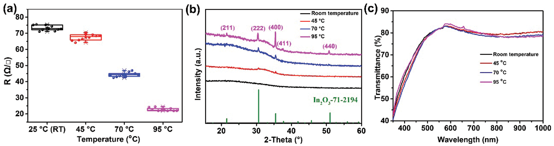
Figure 1: (a) Sheet resistance, (b) XRD patterns, and (c) transmittance spectra of ITO samples sputtered on glass substrates under sputtering temperatures of room temperature (RT), 45°C, 70°C, and 95°C
XRD measurements were performed to study the crystallinity of the ITO films sputtered at different temperatures. The XRD patterns are shown in Fig. 1b. When the film is deposited at room temperature, no characteristic peaks can be assigned to ITO (black line). As the temperature increases, the peaks corresponding to the (222) and (400) crystal planes of ITO gradually increase (red, blue, and magenta lines). This is probably because the higher sputtering temperature can promote the crystallization of the sputtered ITO particles. The transmittance spectra of the sputtered ITO films are shown in Fig. 1c. It can be seen that there was almost no significant difference in the transmittance of ITO films sputtered at different substrate temperatures. Moreover, they all show high transmittance of around 70%∼80% across the visible region. This means the sputtered ITO is suitable for serving as transparent electrodes in the ST-PSCs.
SEM was used to investigate the morphology and microstructure of the sputtered ITO films. The results are presented in Figs. 2a–2d. It can be observed that all of the ITO films are composed of uniform grains. Besides, the grain size of the ITO films strongly depends on the sputtering temperature. As the temperature increases, the grain size is enlarged. This is consistent with the XRD results.
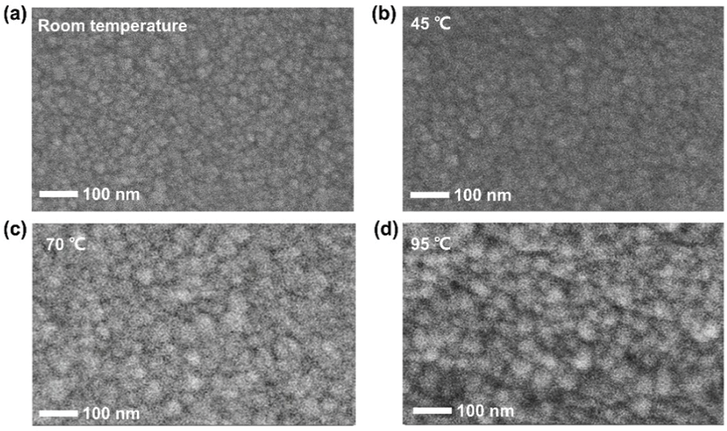
Figure 2: Top-view SEM images of glass/ITO sputtered at room temperature (RT), 45°C, 70°C, and 95°C
To explore the surface roughness of the prepared ITO films, we performed atomic force microscopy (AFM) measurements, and the results are shown in Figs. 3a–3d. The roughness (defined by root mean sheet ) of the films sputtered at room temperature, 45°C, 70°C, and 95°C are 0.549, 1.32, 1.74, and 1.89 nm, respectively. This means the sputtered ITO possesses a very flat surface morphology over these four sputtering temperatures. This is essential for high fill factor (FF) when these films are applied as electrodes in the perovskite solar cells.
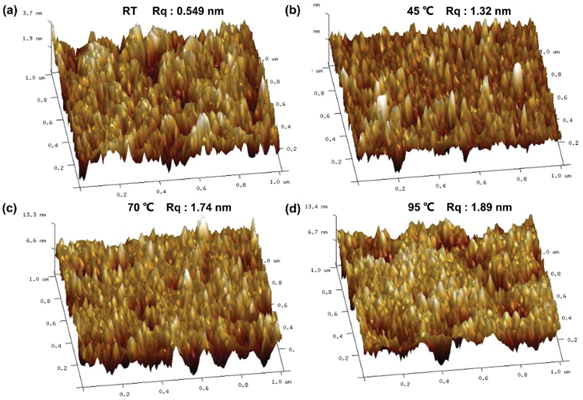
Figure 3: AFM surface morphology and RMS of glass/ITO sputtered at room temperature (RT), 45°C, 70°C, and 95°C
3.2 Device Performance of the ST-PSCs
We utilized the developed ITO sputtering recipe to fabricate ST-PSCs. As shown in Fig. 4a, the architecture of the semi-transparent device is glass/commercialized-ITO/SnO2/perovskite/Spiro-OMeTAD/MoOx/sputtered ITO. Therein, glass/ITO, SnO2, perovskite, Spiro-OMeTAD, and MoOx acts as the cathode, electron transport material, light absorber, hole transport material, and buffer layer, respectively [29,30]. Sputtered ITO film was deposited as the transparent electrode. The cross-sectional SEM was performed to confirm the device structure. The image in Fig. 4b demonstrates a layer-by-layer structure, which shows that the thickness of the perovskite, Spiro-OMeTAD, MoOx, and sputtered ITO layers is about 816, 186, 21, and 127 nm, respectively.
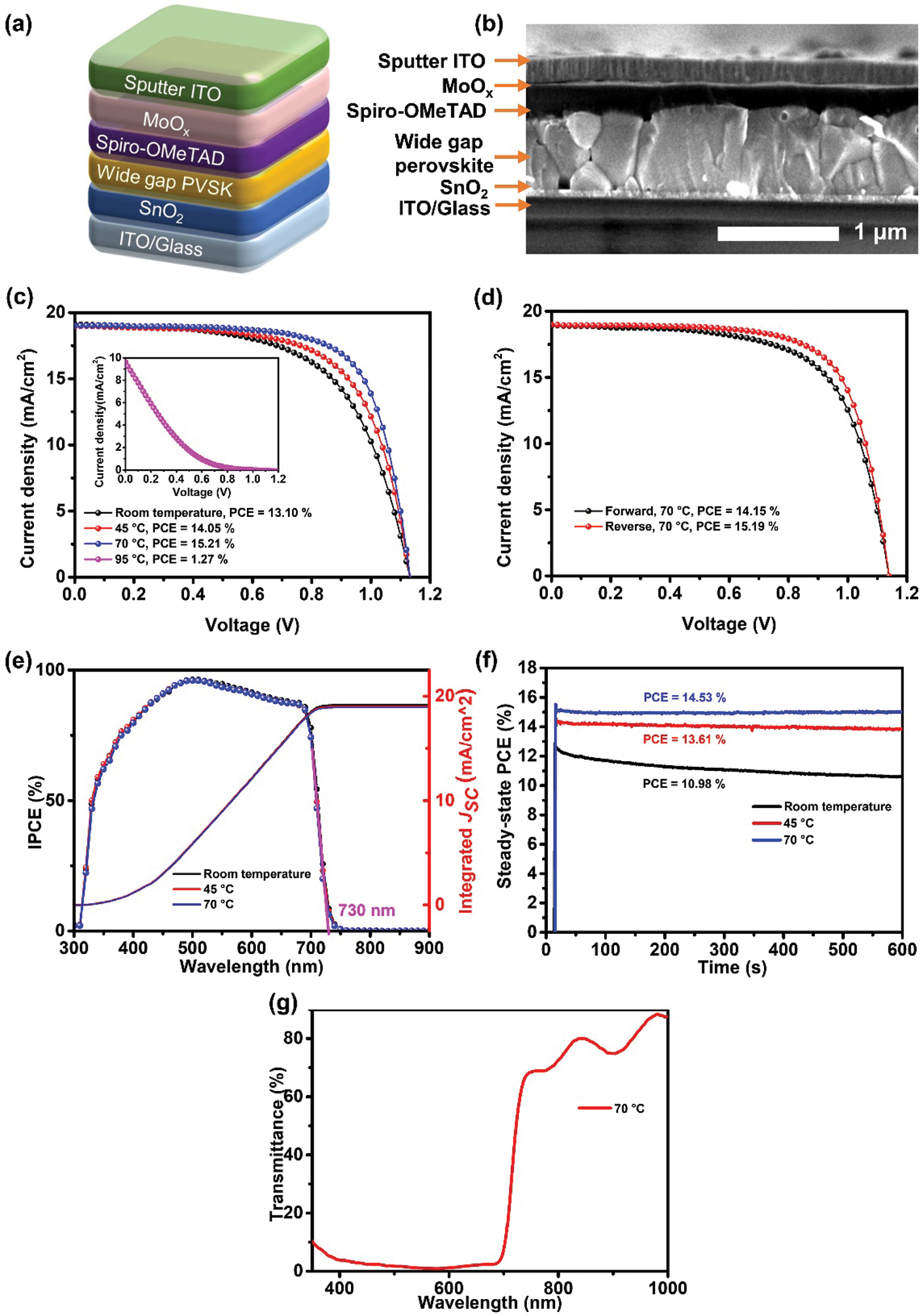
Figure 4: (a) Device architecture and (b) cross-sectional SEM image of the ST-PSC. (c) J–V curves of ST-PSCs with ITO electrodes sputtered at room temperature (RT), 45°C, 70°C, and 95°C. (d) J–V curves of forward and reverse scan for the champion ST-PSCs with ITO electrode sputtered at 70°C. (e) IPCE spectra, and (f) steady-state output at maximum power point (0.82, 0.88, and 0.92 V) of ST-PSCs with ITO electrode sputtered at room temperature (RT), 45°C, and 70°C. (g) Transmittance spectra of ST-PSC with ITO electrodes sputtered at 70°C
Fig. 4c shows the typical current density-voltage (J–V) characteristics of ST-PSCs. The photovoltaic parameters are summarized in Table 1. As the sputtering temperature increases from room temperature to 45°C and 70°C, the corresponding PCE increases from 13.10% to 14.05% and 15.21%. This enhancement is mainly attributed to the improvement of FF from 60.62% to 65.56% and 70.68%. This is consistent with the decline of sheet resistance when increasing the sputtering temperature of ITO electrodes. In contrast, the efficiency of the sample prepared at 95°C is only 1.27%, which is ascribed to the thermal damage of Spiro-OMeTAD.
Hysteresis is a common issue for perovskite solar cells. We studied the hysteresis effect of the ST-PSCs with ITO sputtered at different temperatures. Fig. 4d shows that the hysteresis of our device is low. The PCEreverse (scan from the open circuit to the short circuit) is 15.19%, and the PCEforward (scan from the short circuit to the open-circuit) is 14.15% for the device with the ITO electrode sputtered at 70°C, corresponding to a hysteresis index, defined by (PCEreverse − PCEforward)/PCEforward, of 7.3%. The detailed device parameters extracted from reverse and forward scanned J–V curves are summarized in Table 2.

Incident photon-to-electron conversion efficiency (IPCE) spectra were carried out to study the photovoltaic response of these devices. The results are shown in Fig. 4e. The absorption threshold is obtained by extrapolating the linear part of the IPCE spectra at the long-wavelength region. The bandgap of the perovskite layer of these devices is extracted to be 1.70 eV, which is a typically optimized bandgap for the top cell of perovskite/silicon tandem solar cells. The integrated JSCfrom the IPCE spectra for the devices with ITO prepared at room temperature, 45°C, and 70°C are 19.02, 18.96, and 18.83 mA cm−2, respectively, consistent with the measured JSC extracted from the J–V curves. The steady-state power output at the maximum power point in Fig. 4f demonstrates that the device with ITO sputtered at 70°C exhibits superior light stability under 1 sun illumination than those with ITO sputtered at other temperatures. The result may be due to the relatively higher sputtering temperature can help the diffusion of Sn4+ ions into the In2O3 lattice [28], which is beneficial to generate more carriers and improve the conductivity of the ITO films. This contributes to suppressed charge accumulation and may be responsible for better device stability. To test the semi-transparent properties of the device in the visible-near infrared region, we measured the light transmittance of the device. As shown in Fig. 4g, the transmittance of the device in the near-infrared wavelength range is about 80%. Good light transmittance meets the requirements for the application in perovskite/silicon tandem solar cells.
To check the device reproducibility, the statistics of device performances based on ITO electrodes sputtered at different temperatures are collected and shown in Figs. 5a–5d. It can be observed that as the sputtering temperature increases from room temperature to 45°C and 70°C, the open-circuit voltage (VOC) and short circuit current density (JSC) do not show distinct variation. However, the FF gradually increases, leading to a significant enhancement in the PCE. This improvement in FF and PCE can be attributed to the decrease of the sheet resistance of sputtered ITO, thereby reducing the series resistance (RS) of the device. However, when the sputtering temperature reaches 95°C, the device performance dramatically drops. This is probably due to the direct evaporation of tBP from the doped Spiro-OMeTAD film at 85°C, causing the significant device performance drop [31].
Figure 5: Statistics of the photovoltaic parameters for the ST-PSCs with ITO sputtered at room temperature (RT), 45°C, 70°C, and 95°C. (a) PCE, (b) FF, (c) VOC, and (d) JSC
In summary, this work reports a new method for preparing transparent electrodes for ST-PSCs. By adjusting the sputtering temperature, the crystallinity of the sputtered ITO is largely improved, and the series resistance of ST-PSC is reduced. The device with the transparent electrode sputtered at a mild heating temperature of 70°C shows a much-improved fill factor. Therefore, we obtain a champion device with a PCE of 15.21% and good power output stability at the maximum power point under one-sum illumination.
Author Contributions: Y. Jin performed the experiments and wrote the draft. Z. Fang and L. Yang fabricated perovskite devices. K. Liu and Y. Luo recorded the SEM images. Y. Zhao recorded the AFM images. M. Li fabricated ITO films. H. Feng and B. Deng contributed to optimizing solar cell fabrication. C. Tian contributed to data analysis. C. Cui contributed to some optical measurements. L. Xie, X. Xu, and Z. Wei supervised the project and revised the manuscript. All authors contributed to the discussion.
Funding Statement: This work was financially supported by the National Natural Science Foundation of China (22179042, U21A2078, and 51902110), Natural Science Foundation of Fujian Province (2020J06021, 2019J01057, and 2020J01064), Scientific Research Funds of Huaqiao University, and Promotion Program for Young and Middle-Aged Teacher in Science and Technology Research of Huaqiao University (ZQN-PY607, ZQN-806).
Conflicts of Interest: The authors declare that they have no conflicts of interest to report regarding the present study.
1. Jeong, J., Kim, M., Seo, J., Lu, H., Ahlawat, P. et al. (2021). Pseudo-halide anion engineering for alpha-FAPbI3 perovskite solar cells. Nature, 592(7854), 381–385. DOI 10.1038/s41586-021-03406-5. [Google Scholar] [CrossRef]
2. Yoo, J. J., Seo, G., Chua, M. R., Park, T. G., Lu, Y. et al. (2021). Efficient perovskite solar cells via improved carrier management. Nature, 590(7847), 587–593. DOI 10.1038/s41586-021-03285-w. [Google Scholar] [CrossRef]
3. Kojima, A., Teshima, K., Shirai, Y., Miyasaka, T. (2009). Organometal halide perovskites as visible-light sensitizers for photovoltaic cells. Journal of the American Chemical Society, 131(17), 6050–6051. DOI 10.1021/ja809598r. [Google Scholar] [CrossRef]
4. National Renewable Energy Laboratory (2021). Best Research-Cell Efficiency Chart. https://www.nrel.gov/pv/cell-efficiency.html. [Google Scholar]
5. Shi, B., Duan, L. R., Zhao, Y., Luo, J. S., Zhang, X. D. (2020). Semitransparent perovskite solar cells: From materials and devices to applications. Advanced Materials, 32(3), 1806474. DOI 10.1002/adma.201806474. [Google Scholar] [CrossRef]
6. Wang, R., Huang, T. Y., Xue, J. J., Tong, J. H., Zhu, K. et al. (2021). Prospects for metal halide perovskite-based tandem solar cells. Nature Photonics, 15(6), 411–425. DOI 10.1038/s41566-021-00809-8. [Google Scholar] [CrossRef]
7. Mujahid, M., Chen, C., Zhang, J., Li, C., Duan, Y. (2020). Recent advances in semitransparent perovskite solar cells. InfoMat, 3(1), 101–124. DOI 10.1002/inf2.12154. [Google Scholar] [CrossRef]
8. Zhu, S. J., Yao, X., Ren, Q. S., Zheng, C. C., Li, S. Z. et al. (2018). Transparent electrode for monolithic perovskite/silicon-heterojunction two-terminal tandem solar cells. Nano Energy, 45, 280–286. DOI 10.1016/j.nanoen.2017.12.043. [Google Scholar] [CrossRef]
9. Ho-Baillie, A. W. Y., Zheng, J. H., Mahmud, M. A., Ma, F. J., McKenzie, D. R. et al. (2021). Recent progress and future prospects of perovskite tandem solar cells. Applied Physics Reviews, 8(4), 041307. DOI 10.1063/5.0061483. [Google Scholar] [CrossRef]
10. Chen, B., Ren, N. Y., Li, Y. C., Yan, L. L., Mazumdar, S. et al. (2021). Insights into the development of monolithic perovskite/silicon tandem solar cells. Advanced Energy Materials, 12(4), 2003628. DOI 10.1002/aenm.202003628. [Google Scholar] [CrossRef]
11. Fu, F., Feurer, T., Jager, T., Avancini, E., Bissig, B. et al. (2015). Low-temperature-processed efficient semi-transparent planar perovskite solar cells for bifacial and tandem applications. Nature Communications, 6(8932), 8932. DOI 10.1038/ncomms9932. [Google Scholar] [CrossRef]
12. Park, H. H., Kim, J. Y., Kim, G., Jung, H., Kim, S. et al. (2020). Transparent electrodes consisting of a surface-treated buffer layer based on tungsten oxide for semitransparent perovskite solar cells and four-terminal tandem applications. Small Methods, 4(5), 2000074. DOI 10.1002/smtd.202000074. [Google Scholar] [CrossRef]
13. Wang, H., Dewi, H. A., Koh, T. M., Bruno, A., Mhaisalkar, S. et al. (2020). Bifacial, color-tunable semitransparent perovskite solar cells for building-integrated photovoltaics. ACS Applied Materials & Interfaces, 12(1), 484–493. DOI 10.1021/acsami.9b15488. [Google Scholar] [CrossRef]
14. Yu, L., Shearer, C., Shapter, J. (2016). Recent development of carbon nanotube transparent conductive films. Chemical Reviews, 116(22), 13413–13453. DOI 10.1021/acs.chemrev.6b00179. [Google Scholar] [CrossRef]
15. Chen, C., Liang, J. W., Zhang, J. J., Liu, X. X., Yin, X. X. et al. (2021). Interfacial engineering of a thiophene-based 2D/3D perovskite heterojunction for efficient and stable inverted wide-bandgap perovskite solar cells. Nano Energy, 90, 106608. DOI 10.1016/j.nanoen.2021.106608. [Google Scholar] [CrossRef]
16. Wang, D., Guo, H. L., Wu, X., Deng, X., Li, F. Z. et al. (2021). Interfacial engineering of wide-bandgap perovskites for efficient perovskite/CZTSSe tandem solar cells. Advanced Functional Materials, 32(2), 2107359. DOI 10.1002/adfm.202107359. [Google Scholar] [CrossRef]
17. Hanmandlu, C., Liu, C. C., Chen, C. Y., Boopathi, K. M., Wu, S. H. et al. (2018). Top illuminated hysteresis-free perovskite solar cells incorporating microcavity structures on metal electrodes: A combined experimental and theoretical approach. ACS Applied Materials & Interfaces, 10(21), 17973–17984. DOI 10.1021/acsami.8b04329. [Google Scholar] [CrossRef]
18. Kurdesau, F., Khripunov, G., da Cunha, A. F., Kaelin, M., Tiwari, A. N. (2006). Comparative study of ITO layers deposited by DC and RF magnetron sputtering at room temperature. Journal of Non-Crystalline Solids, 352(9–20), 1466–1470. DOI 10.1016/j.jnoncrysol.2005.11.088. [Google Scholar] [CrossRef]
19. Loper, P., Moon, S. J., de Nicolas, S. M., Niesen, B., Ledinsky, M. et al. (2015). Organic-inorganic halide perovskite/crystalline silicon four-terminal tandem solar cells. Physical Chemistry Chemical Physics, 17(3), 1619–29. DOI 10.1039/c4cp03788j. [Google Scholar] [CrossRef]
20. McMeekin, D. P., Sadoughi, G., Rehman, W., Eperon, G. E., Saliba, M. et al. (2016). A mixed-cation lead mixed-halide perovskite absorber for tandem solar cells. Science, 351(6269), 151–155. DOI 10.1126/science.aad5845. [Google Scholar] [CrossRef]
21. Rombach, F. M., Haque, S. A., Macdonald, T. J. (2021). Lessons learned from spiro-OMeTAD and PTAA in perovskite solar cells. Energy & Environmental Science, 14(10), 5161–5190. DOI 10.1039/d1ee02095a. [Google Scholar] [CrossRef]
22. Seo, J. Y., Akin, S., Zalibera, M., Preciado, M. R., Kim, H. S. et al. (2021). Dopant engineering for spiro-OMeTAD hole-transporting materials towards efficient perovskite solar cells. Advanced Functional Materials, 31(45), 2102124. DOI 10.1002/adfm.202102124. [Google Scholar] [CrossRef]
23. Zhang, C., Ji, C. G., Park, Y. B., Guo, L. J. (2020). Thin-metal-film-based transparent conductors: Material preparation, optical design, and device applications. Advanced Optical Materials, 9(3), 2001298. DOI 10.1002/adom.202001298. [Google Scholar] [CrossRef]
24. Txintxurreta, J., G-Berasategui, E., Ortiz, R., Hernández, O., Mendizábal, L. et al. (2021). Indium tin oxide thin film deposition by magnetron sputtering at room temperature for the manufacturing of efficient transparent heaters. Coatings, 11(1), 92. DOI 10.3390/coatings11010092. [Google Scholar] [CrossRef]
25. Chen, C., Cheng, Y., Dai, Q., Song, H. (2015). Radio frequency magnetron sputtering deposition of TiO2 thin films and their perovskite solar cell applications. Scientific Reports, 5(1), 17684. DOI 10.1038/srep17684. [Google Scholar] [CrossRef]
26. Kim, D. H., Park, M. R., Lee, G. H. (2006). Preparation of high quality ITO films on a plastic substrate using RF magnetron sputtering. Surface & Coatings Technology, 201(3–4), 927–931. DOI 10.1016/j.surfcoat.2006.01.004. [Google Scholar] [CrossRef]
27. Aijo John, K., Philip, R. R., Sajan, P., Manju, T. (2016). In situ crystallization of highly conducting and transparent ITO thin films deposited by RF magnetron sputtering. Vacuum, 132, 91–94. DOI 10.1016/j.vacuum.2016.07.035. [Google Scholar] [CrossRef]
28. Nisha, M., Anusha, S., Antony, A., Manoj, R., Jayaraj, M. K. (2005). Effect of substrate temperature on the growth of ITO thin films. Applied Surface Science, 252(5), 1430–1435. DOI 10.1016/j.apsusc.2005.02.115. [Google Scholar] [CrossRef]
29. Kanda, H., Uzum, A., Baranwal, A. K., Peiris, T. A. N., Umeyama, T. et al. (2016). Analysis of sputtering damage on I–V curves for perovskite solar cells and simulation with reversed diode model. The Journal of Physical Chemistry C, 120(50), 28441–28447. DOI 10.1021/acs.jpcc.6b09219. [Google Scholar] [CrossRef]
30. Qiu, Z. W., Xu, Z. Q., Li, N. X., Zhou, N., Chen, Y. H. et al. (2018). Monolithic perovskite/Si tandem solar cells exceeding 22% efficiency via optimizing top cell absorber. Nano Energy, 53, 798–807. DOI 10.1016/j.nanoen.2018.09.052. [Google Scholar] [CrossRef]
31. Bailie, C. D., Unger, E. L., Zakeeruddin, S. M., Gratzel, M., McGehee, M. D. (2014). Melt-infiltration of spiro-OMeTAD and thermal instability of solid-state dye-sensitized solar cells. Physical Chemistry Chemical Physics, 16(10), 4864–4870. DOI 10.1039/c4cp00116h. [Google Scholar] [CrossRef]
 | This work is licensed under a Creative Commons Attribution 4.0 International License, which permits unrestricted use, distribution, and reproduction in any medium, provided the original work is properly cited. |