| Journal of Renewable Materials |
DOI: 10.32604/jrm.2022.021609
ARTICLE
Pulse Laser Deposition of HfO2 Nanoporous-Like Structure, Physical Properties for Device Fabrication
1Laser and Optoelectronic Engineering Department, University of Technology, Baghdad, Iraq
2Applied Science Department, University of Technology, Baghdad, Iraq
3Al-Mustaqbal University College, Department of Medical Physics, Hillah, Iraq
4Center of Excellence Geopolymer and Green Technology, Faculty of Engineering Technology, Universiti Malaysia Perlis, Perlis, Malaysia
5Department of Civil Engineering, College of Engineering, Cihan University-Erbil, Kurdistan Region, Iraq
*Corresponding Author: Evan T. Salim. Email: evan_tarq@yahoo.com; evan.t.salim@uotechnology.edu.iq
Received: 23 January 2022; Accepted: 17 March 2022
Abstract: The pulsed laser deposition (PLD) technology was used to effectively create conductive nano and micro hafnium oxide with great purity and transparency for (HfO2) nanofilms. In many optoelectronics devices and their applications, the presence of a high dielectric substance like a nano HfO2, between the metal contacts and the substrates was critical. We used the Pulsed Laser Deposition method to fabricate an Al/HfO2/p-Si Schottky barrier diode where the nanostructured HfO2 films as an intermediate layer and varied substrate temperatures. The optical result reveals a high degree of transparency (93%). The optical bandgap of deposited HfO2 films was observed to vary between 4.9 and 5.3 eV, with a value of roughly 5.3 eV at the optimal preparation condition. The morphology of the surface shows a high homogeneous nano structure with the average values of the roughness about (0.3 nm). With regard to substrate temperature, the produced factor ideality for fabricated diode was determined to be lowering and the associated values of the barrier height rose based on I-V characterization. With regard to substrate temperature, the produced factor ideality for fabricated diode was determined to be lowering and the associated values of the barrier height rose based on I-V characterization. The diode manufactured at 600°C, in particular, had a higher ideality factor value (n = 3.2).
Keywords: Pulse laser deposition; nano films; optoelectronics; HfO2; optical device
The solar cell business is dominated by crystalline silicon-based solar cells, with mono crystalline and multi-crystalline solar cells having the highest proven efficiency of 26.7 percent and 22.3 percent, respectively [1]. Hafnium oxide (HfO2), is a desirable material for optical applications because of its superior optical and electrical characteristics, including a broadly visible band gap, a high induced laser damage threshold, good thermal stability, low reflectivity, and high transmittance [2]. HfO2 has interested researchers due to its excellent physical qualities, which include strong durability, high corrosion resistance, scratch resistance, and good surface roughness [3].
Hafnium oxide nanostructure is one of the most promising materials with a high value of dielectric constant ranging about (15–50) and an optical band-gap value of less than 5 eV, as also it has high chemical stability at the high range of the temperatures and, it has a high thermal conductivity [4,5]. In comparison to TiO2 and Ti2O5, HfO2 has a high reflective index of 2 [6,7], finally, at 1000 K, HfO2 with the silicon has a high value of reaction-free energy about 79.6 kcal/mol [8,9]. In general, three different phases for the nano-monoclinic HfO2 has been recognized, (stable phase) at the low value of temperatures [10,11], the tetragonal phase (which becomes stable at 1720°C), and cubic (which be more stable at 2600°C) [12,13].
In addition, the above properties of this material make it high-refectory material with outstanding properties, leading to the usage of HfO2 in a wide range of applications [14,15]. One of the most important applications is the use of this material as a gas sensor, where Er et al. [16] recognized an enhancement in the sensitivity after 30 min of UV radiation, they observed that the values of the HfO2 nano-films sensitivity are increased, indicating that these nanofilms capacity to be appropriate for sensing gas following UV rays [17,18]. HfO2 is an excellent NO2 gas sensor due to its low cost and chemical and thermal stability [19,20]. HfO2 are combined or doped with the Oxide of silicon in several manufacturing and applications due to its dielectric constant [21,22] since the addition of doping plays an important role in material properties [23]. Placement of oxide in silicon on the Devices made of metals over oxides over semiconductors (MOS) in the access memory dynamic for the fabricated devices and the stack gate is one of the main applications of HfO2 [24,25].
Other work on the same material shows the use of HfO2 as a heat mirror. A heated mirror was built based on the hafnium oxide/silver/hafnium oxide/glass system. This heat mirror was found to be transparent in the visible with an average transmittance of 72.4%, and reflective in the near-infrared (wavelength = 700–2000 nm) with an average reflectance of 67.0% [26]. Up to our best knowledge, the HfO2 Nanofilms on Si substrate as a heterojunction photodetector has not been extensively studied yet, as a result, in this manuscript, a HfO2/Si hetero-junction device was prepared and characterized after the preparation and characterization of the HfO2 films at different temperatures.
Both HfO2 and hafnium (IV) chloride (with purity 99.9999% and 99%) sequentially were obtained from Sigma Aldrich. Three grams of HfO2 were used to prepare the disk in dimensions (2 × 0.5) cm as shown in Fig. 1. The hydraulic press was used to press HfO2 powder to prepare the disk in 1 Ton. The processes of the experimental for PLD are presented in Fig. 2, where the PLD system uses the Nd:YAG (Q-switch laser) and its characteristics that presented in Table 1. The Genetic Joule-meter QE12 is used to calibrate the laser energy.

Figure 1: HfO2 after pressing

Figure 2: The experimental set up of pulsed laser deposition
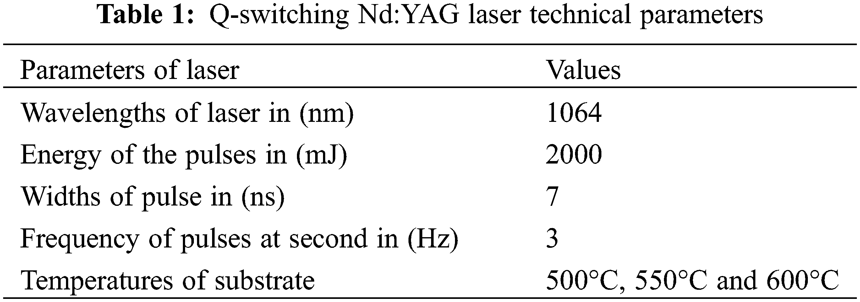
At room temperatures, the Nd:YAG Q-switching Laser was used at varying temperatures of the substrate, 2 J energy, and pulses numbers of 400 pulses. The laser device and the deposition chamber are the two most important parts of the PLD system. The deposition using pulsed laser process was conducted in a chamber of vacuum with a vacuum of around 10−3 Torr. The concentrated Nd:YAG (second harmonic generation) SHG Q-switching laser beam makes a 45° angle with the target surface. The deposited nano-films were formed on the substrates of quartz at temperatures of 500, 550, and 600°C and with a laser intensity of 2000 mJ. The Q switched Nd:YAG laser was used to deposit 50 shots with varying substrate temperatures and a pulse repetition rate of 6 Hz. The target was constructed as a disk before the thin film was applied. The target was formed as a disk with a diameter of 2 cm and a thickness of 0.5 cm, with the purity of HfO2 (99.9%) supplied by Gamma. Characterizations were explored utilizing a variety of measuring techniques, including XRD, SEM, and AFM measurements; for assessing the shape and the deposited Nano-thin film structure.
2.1 Preparation of HfO2 Thin Films
Before starting to deposit the samples, there are two important steps that have to be done. The first one is: all the substrates were cleaned by using isopropyl alcohol, detergent solution and washed by acetone after washed by deionized water cleaned the substrate (quartz) and this includes. Later the HfO2 (high-quality) nano-films were deposited inside the vacuum chamber at different temperatures of the substrate about 500, 550, and 600°C by using the PLD technique.
2.2 Hetero-Junction Diode Made of Al/HfO2/n-Si
Type Al/HfO2/n-Si hetero-junction diodes were made on a silicon wafer (n-type, Si100) with a resistance of 0–30 cm and a thickness of 250 μm. But in usual some impurities, for example, dust, grease, oil, etc., can be found on the surface of Si-wafer, so it was necessary to clean the substrate before fabricating the Schottky diode. On the other hand, the cleaning process can affect positively on the parameters of a diode as presented in the investigation [18]. The deposited homogeneous HfO2 nano-films and structure on the selected substrates (n-type Si) at varying temperatures of the substrate ranging from 400 to 600 degrees Celsius. Pure aluminum was sputtered on the deposited HfO2/n-Si using (dc sputtering) with a square mask 1 × 1 cm and its thickness around 200 nm to establish a contact.
X-ray diffraction was used to study the phase transformation of the thin films with wavelength 0.15406 nm of Cukα1 (Rigaku Miniflex-II). While FE-SEM (Zeiss Sigma) was used to study the surface morphology and compositional analysis of the samples. The optical properties of the films were examined by photoluminescence spectroscopy (FP/8300) and UV-Vis spectroscopy (JASCO Model No. V-770PC) and A Keithley Electrometer was used to measure current-voltage properties (Model No. 6517-B).
Fig. 3 illustrates the XRD pattern of hafnium oxide films deposited at temperatures of 500, 550, and 600°C. It is clear that as the deposition temperature increase, the HfO2 films become more crystallized. Two different crystalline phases could be recognized, the cubic and the monoclinic. The transformation in film structure from amorphous as shown at 500°C to be more crystalline at 550°C, could be seen in Fig. 3.

Figure 3: XRD of nano HfO2 films at substrates at temperature (a) 500°C, (b) 550°C, and (c) 600°C
The enhanced in crystallinity of the film is related to increasing the molecule thermal energy at elevated temperature resulting in more chance for each molecule or atom to reconnect with its neighbored molecule to build the crystal at a specific structure and phase. At the low temperature, the atoms slowly stick and harden to form an amorphous film. Relatively and at the low temperature, the substrate molecules have a low value of the kinetic energy, the creation of the (long range-orientation) (LRO) for molecules [7,8,27]. The monoclinic crystal structure of the Hafnium (IV) oxide films was seen at 500, 550, and 600°C, and these results are consistent with (JCPDS) data number of (78–0049) at a = 5.117, b = 5.175, and c = 5.291. significantly, it has been noticed that there is an increase in the (–111) and (111) plans diffraction intensity with increasing the temperature from 500 to 600°C was which was produced by atom diffusion, resulting in combining large numbers of atoms coming together, and hence an increase in grain size could be recognize this behavior agree with other work [7,8,28]. Fig. 3 depicts the transition from amorphous to monoclinic phase for temperatures between 500 and 600 degrees Celsius. This shows that the temperature of the substrate has an influence on the HfO2 films. The transition to the crystalline phase was predicted, as previously stated [7,8,29]. The following equations were used to compute the structural characteristics of HfO2 films [30–32]:
where ε is the strain, δ is dislocation density, SF is the stacking faults, all the values of these parameters are listed in Table 2.
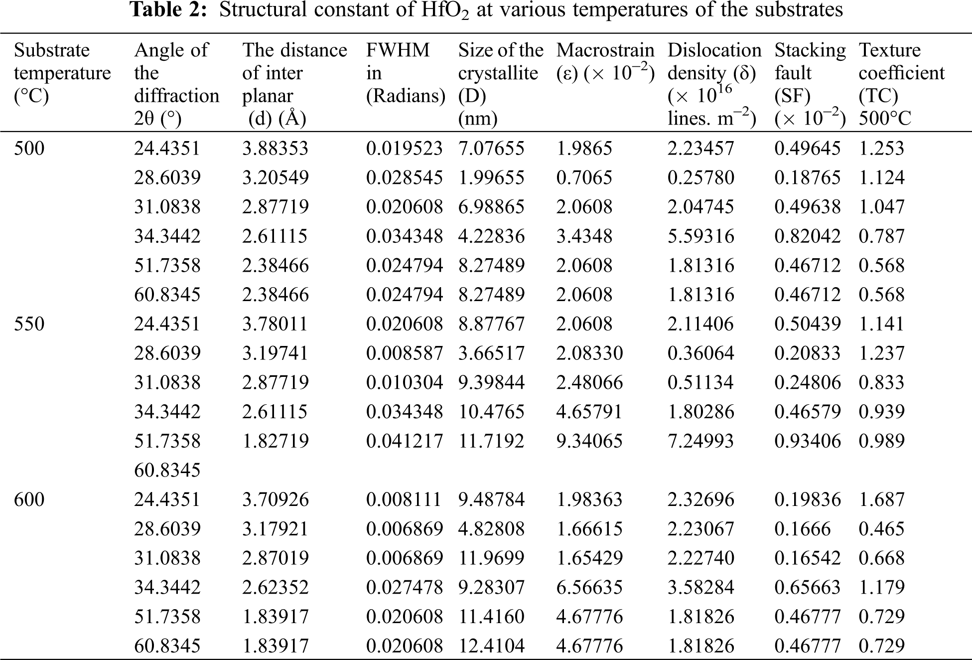
In addition, it has been found that the sizes of the crystallite equal 6.98865, 9.29844, and 11.9699 nm for 500, 550, 600°C, respectively.
The amended size of crystallite with a high temperature of the substrate belongs to the mobility of the atoms and low density of packing which was values of the influenced by the temperature of the substrate [7,8,33]. In general, the increase in the substrate temperature from 500 to 600°C led to reducing the stacking fault and the strain because of reducing the blemishes at the grain’s interfaces as a result of the oxygen vacancies [7,8,34]. Fig. 3 shows the difference in structural parameters in various temperatures. It might be the cause of the lower stacking fault and strain readings as the temperature rises. Furthermore, with temperature, the predicted mean values of the (dislocation density) changed from 2.04745 × 10¹⁶ to 2.22740 × 10¹⁶ lines m−2. The characteristics of the structure for HfO2 nano-films were greatly enhanced above 550°C, according to the XRD data. As a result, altering the structure of the samples may improve the films’ electrical and optical characteristics.
Furthermore, X-ray diffraction revealed that as the deposition temperature was raised, the intensity values of the presented peaks of 011, 100, 111, 002, 220, and 302 are increasing. In addition, AFM pictures of Hafnium oxide films indicated that the grain size grew with the substrate’s temperature from 18 to 86 nm, but the values of the roughness are reduced, as a result of substrate temperatures effect, as presented in below Fig. 4.

Figure 4: Grain size and the roughness for HfO2 nano films at different substrates temperature
In general, roughness rises as grain size grows, however roughness reduced as grain size grew in this study. This might be related to the manner of deposition. The thickness, on the other hand, maybe determined using AFM scans of the film increased from 47 to 102 nm at 500°C and 550°C, respectively [7,8,35], as shown in Fig. 5.

Figure 5: LPD produced HfO2 films at various temperatures
The transmission declined as the deposition temperature increased, while the absorbance values are increased as presented in the Figs. 6 and 7. The highest transmittance values occurred as the approached wavelength at the Near Infra-Red area, as indicated in the Fig. 6, while the maximum values of the absorption emerged around the Near Infra-Red region. As shown in the presented Fig. 7, HfO2 films have an absorbance range of (1.51–1.94) percent and transmission spectra of (73–84) percent, these results agree with other work [36].

Figure 6: The absorbance spectra of HfO2 nano-films at various temperatures

Figure 7: HfO2 film transmittance spectra at various temperatures
Fig. 8 present the optical energy band gap of HfO2 nanofilms made at 500, 550, and 600°C, with the energy gap of HfO2 being about (4.9–5.3) eV. It can be seen in Fig. 8 that the Eg dropped as the temperature was increased, going from 5.3 to 4.9 eV. Because of the decrease in Eg, intermediate levels between the valence and conduction bands were shared, these results agree with other work [37].

Figure 8: Optical energy gab for HfO2 nano films at various temperatures
Fig. 9 presents a significant emission at the wavelength range of 337 to 365 nm where the PL spectra of Hafnium dioxide films at various substrate temperatures (500, 550, and 600°C) have been given. It is clear that as increasing the substrate temperature the emission wavelength of films was improved. At 500°C a weak emission could be shown at 337 nm, while it has been increasing to 365 nm at a higher substrate temperature of about 600°C which is related to the lower recombination of charge carriers and the oxygen vacancies [7,8]. The films coated at 600°C emitted a substantial amount of light at 365 nm, which might imply that the energy in the films decreases and the wavelength increases as the temperature rises as a result of the density low-packing, which causes the voids empty to develop between the values of the grain of the surfaces. Interestingly, previous studies [7,8] found a similar pattern of increased intensity of the PL with increasing temperature substrate.

Figure 9: The photoluminescence results for nano HfO2 films at various temperatures
Fig. 10 shows 2D and 3D AFM images of HfO2 nano-films that were deposited at different temperatures with the scan area 4 μ × 4 μ, and the films’ height increased with increase in the temperature of the substrates.

Figure 10: 2D and 3D AFM images of HfO2 at different temperatures
FE-SEM was used to determine the surface structure, grain orientation, and shape of these thin films. Fig. 11 shows FE-SEM images for the deposited HfO2 nano-films are prepared and deposited on several substrates at temperatures ranging from 500 to 600 degrees Celsius. The HfO2 films produced a honeycomb/micro-porous like structure at 500 degrees Celsius, with fewer figures of grains (like balls) with a diameter of 3–4 m, as reported previously at the same figure. Furthermore, when the temperature of the substrate samples was raised to 550°C, the number of ball-like grains rose as well. Due to the gathering, and the agglomeration of the nano-grains after impacting against the heated substrate, they mix and form big grains [7,8]. Furthermore, a clump of the grains is closely bound as presented in Fig. 11 due to the sluggish nucleation rate. Large numbers of ball-like grains may be detected at a higher substrate temperature of 600°C compared to other temperatures. It is also worth noting that the size of the holes shrinks from 10 to 100 nm, resulting in a nano porous-like morphology. Higher temperatures, according to this conclusion, promote grain development and decrease the pore’s structure sizes are found in the presented samples. The surface morphology of HfO2 films is supported by the shift in the structure of the crystal from the amorphous structures to the monoclinic structures. The diode factors will be improved by a (pores-like) structure at a higher number of the channel.

Figure 11: SEM images of HfO2 thin films at various substrate temperatures; (a–c) the samples were examined by Image J; (d–f) show the distribution of the diameters of HfO2
Fig. 11 The SEM of HfO2 at different temperature substrates and it has been noticed that the average size of the particles between (5–9.9) nm rose at the highest temperature of the substrate 600°C compare to 500°C and 550°C.
3.5 Energy Dispersive X-Ray Spectroscopy (EDX)
Fig. 12 shows the EDX picture of the deposited HfO2 nano-films with the different temperature substrates. The presences of Hf and oxygen (O) components in the films are shown by the EDX spectra. A clear increase in Hf atomic weight with a reduction in oxygen atomic ratio could be recognized as the substrate temperature was increased from 500°C to 600°C which give rise to enhanced stoichiometry, Finally, all of the deposited films show excellent stoichiometry characteristics. Additionally, the MIS diode’s electrical activity will be reinforced by the constant lowering of oxygen (atomic percent).

Figure 12: EXD analysis of HfO2 nano-films at different temperature of the substrates
3.6 Schottky Barrier Diode Al/HfO2/n-Si Characterization
Hafnium dioxide Nanostructures layer was deposited on the Si wafer P-type and deposited a mask of Aluminum up to the HfO2 nanostructure to fabricate the optoelectronic device. The voltage-current (I-V) characterization of the deposited (Al/HfO2/p-Si) at various temperatures of the substrates are presented in Fig. 13. The I-V results will be used to investigate contacts of the Schottky, the quality interface, device performance, and constraints. The reverse and forward current levels of the manufactured device were tested using a continuous biasing voltage ranging from –3 to +3 V. For all of the fabricated diodes, the observed forward current grows exponentially with voltage and demonstrates good rectification behavior. Reverse current is reduced, while forward current development is exponential at 600°C substrate temperature, suggesting improved rectification capabilities and the excellent nature of the deposited and manufactured devices (diodes). The contact/junctions (Metal-semiconductor) MS and the semiconductor hetero-junction that is comparable configurations generate a barrier Schottky. A Schottky diode is another name for an MS contact. In these facilities, the majority of charge carriers are in charge of carrier transit. The current-voltage characteristics are studied throughout a wide temperature range to explore the current transport mechanism in these devices. The intercept and the slope of the J-V curve (semi-logarithmic) are used to calculate the barrier height and ideality factor using the theory of the thermionic-emission. The current via Al/HfO2/P-Si was defined using the following equations according to the theory of the thermionic-emission [38–40]:
The diode’s reverse saturation current, Io, was computed.
Where Io stands for reverse saturation current, q stands for electron charge, V stands for bias voltage, n stands for ideality factor, B stands for effective barrier height, KB stands for Boltzmann constant, T stands for temperature, A stands for diode area, and A* stands for the constant of the effective-Richardson. The value of the Io is a parameter of the fabricated diode that represents reverse saturation current and minority carrier diffusion in the depletion area at forwarding bias. The value of the Io for the fabricated diode is increasing with the temperature of the substrate, from Io = 515.2 mA at 500°C to Io = 1140.5 mA at 600°C, among three based voltages.

Figure 13: I-V characteristics of Al/HfO2/p-Si barrier hetero-structure devise
Using the ln J vs. voltage plot (Fig. 14) and the following equation to estimate the Al/HfO2/p-Si diodes’ ideal factors (n) and barrier heights (experimental values) [41–44], the forward bias’s slopes and intercept were calculated.

Figure 14: Density of current (ln J) with the applied voltage (V) for the fabricated device
As the temperatures of the substrate are rises, the calculated values of the factor (ideality) were calculated to be dropping and the associated height barrier was increasing. At low temperatures of the substrate, the electrons can overcome the lower value of the barriers or the patches. As a result, the values of current flowing through patches with lower barrier height and a greater ideality factor will dominate current transport. As the temperature rises, more electrons have enough energy to break through the higher barrier. In this situation, the height of the barrier will rise as the temperature rises [45,46]. The Al/HfO2/p-Si diode produced at 600°C has a minimum value of the (ideality) factor of 3.2 and matches with the height of the barrier equal to B = 0.824 eV. According to Altndal et al., the lower of n results in a greater B value at higher temperatures [47,48]. Similarly, a number of research groups have reported temperature-dependent Schottky diodes made using diverse techniques [47,48]. Many studies have also described the dependent-temperature based on the Schottky device made using different techniques [48,49]. Because of the thermionic emission sample, the electron does not have enough energy to pass throw the barrier energy at a lower temperature of the substrates, however, at a maximum substrate temperature, the higher values of barriers are readily overcome by the electron. As a result, most diodes operate better at higher temperatures [50,51].
HfO2 nano and microstructures were successfully deposited utilizing the PLD approach using high values of the quality-wide-band gap HfO2 Nano-thin films on a quartz substrate at varying temperatures of the substrate. Furthermore, the best film in terms of absorbance, transmission, the thicknesses of the Nano-film, and founds have a significant impact on the characteristics and performance of photonics and optoelectronic devices. The coated films’ physical characteristics (optical, structural, and electrical) were investigated. The XRD data for HfO2 suggest a monoclinic crystal structure, with the crystallite improving after 550°C. The FE-SEM micrograph revealed ball-like grains and micro-porous structures. Furthermore, at 600°C, a considerable of grains numbers with a tiny porous structure has been observed. The presence of O and Hf was verified by EDX analyses which insure the formation of stoichiometric material. At 600°C, thin films of HfO2 exhibit an absorption peak with a band gap of 3.41 eV. Meanwhile, an emission significant peak at 384 nm was discovered in the PL spectra and at high temperatures. The I-V test revealed that increasing the temperature of the substrate lowers the values of the ideality-factor and strengthens the (barrier-heights), as well as inverting the Al/HfO2/n-Si diode’s saturation current. The fabricated device insure the fact that HfO2 is a versatile material for hetero-junction device fabrication as a photodiode or solar cell, the device performance study reflects a good rectification behavior with enhanced properties with temperature.
Acknowledgement: The authors would like to thank the Department of Laser Engineering and Electro-Optic/University of Technology for the logistic support this work.
Funding Statement: The authors received no specific funding for this study.
Conflicts of Interest: The authors declare that they have no conflicts of interest to report regarding the present study.
1. Martin, A. G., Ewan, D. D., Dean, H. L., Jochen, H., Masahiro, Y. et al. (2019). Solar cell tables (version 54). Progress in Photovoltaics: Research and Applications, 27(7), 565–575. DOI 10.1002/pip.3171. [Google Scholar] [CrossRef]
2. Martínez-Merlín, I., Guzmán-Mendoza, J., García-Hipólito, M., Sánchez-Resendiz, V. M., Lartundo-Rojas, L. et al. (2016). Transparent and low surface roughness HfO2: Tb3+, Eu3+ luminescent thin films deposited by USP technique. Ceramics International, 42(2), 2446–2455. DOI 10.1016/j.ceramint.2015.10.045. [Google Scholar] [CrossRef]
3. Bright, T. J., Watjen, J. I., Zhang, Z. M., Muratore, C., Voevodin, A. A. (2012). Optical properties of HfO2 thin films deposited by magnetron sputtering: From the visible to the far-infrared. Thin Solid Films, 520(22), 6793–6802. DOI 10.1016/j.tsf.2012.07.037. [Google Scholar] [CrossRef]
4. Mohsin, M. H., Numan, N. H., Salim, E. T., Fakhri, M. A. (2021). Physical properties of sic nanostructure for optoelectronics applications. Journal of Renewable Materials, 9(9), 1519–1530. DOI 10.32604/jrm.2021.015465. [Google Scholar] [CrossRef]
5. Lin, S. S., Liao, C. S., Fan, S. Y. (2015). Effects of substrate temperature on properties of HfO2, HfO2:Al and HfO2:W films. Surface and Coatings Technology, 271, 269–275. DOI 10.1016/j.surfcoat.2014.10.057. [Google Scholar] [CrossRef]
6. Salim, E. T., Khalid, F. G., Fakhri, M. A., Mahmood, R. S. (2021). Laser wavelength effects on the optical, structure, and morphological properties of nano HfO2 structures. Materials Today: Proceedings, 42, 2422–2425. DOI 10.1016/j.matpr.2020.12.551. [Google Scholar] [CrossRef]
7. Basel, S., Numan, N. H., Khalid, F. G., Fakhri, M. A. (2020). Structure and optical properties of HfO2 nano films grown by PLD for optoelectronic device. AIP Conference Proceedings, vol. 2213, 20228. DOI 10.1063/5.0000185. [Google Scholar] [CrossRef]
8. Lauria, A., Villa, I., Fasoli, M., Niederberger, M., Vedda, A. (2013). Multifunctional role of rare earth doping in optical materials: Nonaqueous sol-gel synthesis of stabilized cubic HfO2 luminescent nanoparticles. ACS Nano, 7, 7041–7052. DOI 10.1021/nn402357s. [Google Scholar] [CrossRef]
9. Makram, A. F., Evan, T. S., Ahmed, W. A., Hashim, U., Mohammed, A. M. et al. (2019). The effect of annealing temperature on optical and photolumence properties of LiNbO3. Surface Review and Letters, 26(10), 1950068. DOI 10.1142/S0218625X19500689. [Google Scholar] [CrossRef]
10. Kumar, G. M., Ilanchezhiyan, P., Fu, X., Siva, C., Kumar, A. M. et al. (2016). Blue luminescence and Schottky diode applications of monoclinic HfO2 nanostructures. RSC Advances, 6, 57941–57947. DOI 10.1039/C6RA10644G. [Google Scholar] [CrossRef]
11. Liang, H. L., Jin, X., Da, Y. Z., Ren, S. Q. (2021). Phase transformation and dielectric properties of Y doped HfO2 thin films. Journal of Alloys and Compounds, 861, 158241. DOI 10.1016/j.jallcom.2020.158241. [Google Scholar] [CrossRef]
12. Jayaraman, V., Bhavesh, G., Chinnathambi, S., Ganesan, S., Aruna, P. (2014). Synthesis and characterization of hafnium oxide nanoparticles for bio-safety. Materials Express, 4, 375–383. DOI 10.1166/mex.2014.1190. [Google Scholar] [CrossRef]
13. Chen, G. H., Hou, Z. F., Gong, X. G., Li, Q. (2008). Effects of Y doping on the structural stability and defect properties of cubic HfO2. Journal of Applied Physics, 104, 74101. DOI 10.1063/1.2985908. [Google Scholar] [CrossRef]
14. Fakhri, M. A., Basheer, R. A., Banoosh, A. M., Azeez, H. N. (2021). Rapid thermal oxidation of nano silver film for solar cell fabrication. Digest Journal of Nanomaterials and Biostructures, 16(2), 367–375. [Google Scholar]
15. Quintero-García, J. S., Puente-Urbina, B. A., García-Cerda, L. A., Rodríguez-Fernández, O. S., Mendoza-Mendoza, E. A. (2015). A “Green methodology” approach to the synthesis of HfO2 nanoparticles. Materials Letters, 159, 520–524. DOI 10.1016/j.matlet.2015.07.014. [Google Scholar] [CrossRef]
16. Er, I. K., Çağırtekin, A. O. (2021). Synthesis of Al/HfO2/p-Si Schottky diodes and the investigation of their electrical and dielectric properties. Journal of Materials Science: Materials in Electronics, 32, 1677–1690. [Google Scholar]
17. Al-Douri, Y., Makram, A. F., Bouhemadou, A., Khenata, R., Ameri, M. (2018). Stirrer time effect on optical properties of nanophotonic LiNbO3. Materials Chemistry and Physics, 203, 243–248. DOI 10.1016/j.matchemphys.2017.10.024. [Google Scholar] [CrossRef]
18. Kumar, N., George, B. P. A., Abrahamse, H., Parashar, V., Ngila, J. C. (2017). Sustainable one-step synthesis of hierarchical microspheres of PEGylated MoS2 nanosheets and MoO3 nanorods: Their cytotoxicity towards lung and breast cancer cells. Applied Surface Science, 396, 8–18. DOI 10.1016%2Fj.apsusc.2016.11.027. [Google Scholar]
19. Abood, M. K., Salim, E. T., Saimon, J. A. (2018). Niobium pentoxide thin film prepared using simple colloidal suspension for optoelectronic application. International Journal of Nanoelectronics and Materials, 11(2), 127–134. [Google Scholar]
20. Chandran, P. R., Sandhyarani, N. (2014). An electric field responsive drug delivery system based on chitosan-gold nanocomposites for site specific and controlled delivery of 5-fluorouracil. RSC Advances, 4, 44922–44929. DOI 10.1039/C4RA07551J. [Google Scholar] [CrossRef]
21. Manimekalai, K., Padmamalini, N., Vinitha, G., Jayaprakash, P. (2022). Crystal growth and physico-chemical characterization of methyl ammonium chloride doping on the characteristics of potassium dihydrogen. Inorganic Chemistry Communications, 137, 109207. DOI 10.1016/j.inoche.2022.109207. [Google Scholar] [CrossRef]
22. Abutalib, M. M., Rajeh, A. (2021). Enhanced structural, electrical, mechanical properties and antibacterial activity of Cs/PEO doped mixed nanoparticles (Ag/TiO2) for food packaging applications. Polymer Testing, 93, 107013. DOI 10.1016/j.polymertesting.2020.107013. [Google Scholar] [CrossRef]
23. Mohammed, D. A., Fakhri, M. A., Kadhim, A. (2018). Reduction the corrosion rate of 304 stainless steel using pulsed laser shock penning method. IOP Conference Series: Materials Science and Engineering, 454(1), 012162. DOI 10.1088/1757-899X/454/1/012162. [Google Scholar] [CrossRef]
24. Al-Kuhaili, F. (2004). Optical properties of hafnium oxide thin films and their application in energy-efficient windows. Optical Materials, 27(3), 383–387. DOI 10.1016/j.optmat.2004.04.014. [Google Scholar] [CrossRef]
25. Abood, M. K., Salim, E. T., Saimon, J. A. (2018). Impact of substrate type on the microstructure of H-Nb2O5 thin film at room temperature. International Journal of Nanoelectronics and Materials, 11(Special Issue), 55–64. [Google Scholar]
26. Makram, A. F., Mohammed, J. A., Ali, A. A., Wijdan, H. M. (2020). Theoretical study of a pure LinbO3/Quartz waveguide coated gold nanorods using supercontinuum laser source. Optical Materials, 109, 110363. DOI 10.1016/j.optmat.2020.110363. [Google Scholar] [CrossRef]
27. Sun, N. N., Zhou, D. Y., Liu, W. W., Zhang, Y., Li, S. D. et al. (2021). Importance of tailoring the thickness of SiO2 interlayer in the observation of ferroelectric characteristics in yttrium doped HfO2 films on silicon. Vacuum, 183, 109835. DOI 10.1016/j.vacuum.2020.109835. [Google Scholar] [CrossRef]
28. Raid, A. I., Bassam, G. R., Evan, T. S., Mukram, A. (2007). Transparent and conducting ZnO films prepared by reactive pulsed laser deposition. Journal of Materials Science: Materials in Electronics, 18(4), 397–400. DOI 10.1007/s10854-006-9046-y. [Google Scholar] [CrossRef]
29. Suvorova, E. I., Uvarov, O. V., Arkharova, N. A., Ibrayeva, A. D., Skuratov, V. A. et al. (2020). Structure evolution, bandgap, and dielectric function in La-doped hafnium oxide thin layer subjected to swift Xe ion irradiation. Journal of Applied Physics, 128(16), 164103. DOI 10.1063/5.0025536. [Google Scholar] [CrossRef]
30. Alaa, A. A., Farhad, M. O., Makram, A. F. (2021). Preparation of MgO-MnO2 nanocomposite particles for cholesterol sensors. Journal of Materials Science: Materials in Electronics, 32, 15523–15532. DOI 10.1007%2Fs10854-021-06102-2. [Google Scholar]
31. Evan, T. S. (2013). Surface morphology and X-ray diffraction analysis for silicon nanocrystal-based heterostructures. Surface Review and Letters, 20(5), 1350046. DOI 10.1142/S0218625X13500467. [Google Scholar] [CrossRef]
32. Rauwel, P., Augustinas, G., Ducroquet, F., Rauwel, E. (2019). Selective photocurrent generation in HfO2 and carbon nanotube hybrid nanocomposites under Ultra-Violet and visible photoexcitations. Materials Letters, 246, 45–48. DOI 10.1016/j.matlet.2019.03.030. [Google Scholar] [CrossRef]
33. Alhasan, S. F. H., Bader, B. A., Salim, E. T. (2021). Surface morphology and roughness of silver oxide prepared employing pulsed laser at optimum laser fluence. Materials Today: Proceedings, 42, 2845–2848. DOI 10.1016/j.matpr.2020.12.732. [Google Scholar] [CrossRef]
34. Martínez, F. L., Toledano-Luque, M., Gandía, J. J., Cárabe, J., Bohne, W. et al. (2007). Optical properties and structure of HfO2 thin films grown by high pressure reactive sputtering. Journal of Physics D: Applied Physics, 40, 5256. DOI 10.1088/0022-3727/40/17/037. [Google Scholar] [CrossRef]
35. Papernov, S., Brunsman, M. D., Oliver, J. B., Hoffman, B. N., Kozlov, A. A. et al. (2018). Optical properties of oxygen vacancies in HfO2 thin films studied by absorption and luminescence spectroscopy. Optics Express, 26, 17608–17623. DOI 10.1364/OE.26.017608. [Google Scholar] [CrossRef]
36. Alsultany, F. H., Alhasan, S. F. H., Salim, E. T. (2021). Seed layer-assisted chemical bath deposition of Cu2O nanoparticles on ITO-coated glass substrates with tunable morphology, crystallinity, and optical properties. Journal of Inorganic and Organometallic Polymers and Material, 31, 3749–3759. DOI 10.21203/rs.3.rs-217173/v1. [Google Scholar] [CrossRef]
37. Padma, K. H., Vidya, S., Saravana, K. S., Vijayakumar, C., Thomas, J. K. (2015). Optical properties of nanocrystalline HfO2 synthesized by an auto-igniting combustion synthesis. Journal of Asian Ceramic Societies, 3(1), 64–69. DOI 10.1016/j.jascer.2014.10.009. [Google Scholar] [CrossRef]
38. Nahar, R. K., Vikram, S., Aparna, S. (2007). Study of electrical and microstructure properties of high dielectric hafnium oxide thin film for MOS devices. Journal of Materials Science: Materials in Electronics, 18, 615–619. DOI 10.1007/s10854-006-9111-6. [Google Scholar] [CrossRef]
39. Raid, A. I., Evan, T. S., Halemah, T. H. (2021). Preparation of Nb2O5 nanoflakes by hydrothermal route for photodetection applications: The role of deposition time. Optik, 245, 167778. DOI 10.1016/j.ijleo.2021.167778. [Google Scholar] [CrossRef]
40. Hector, G., Helena, C., Salvador, D., Luis, B., Francesca, C. et al. (2013). Electrical characterization of atomic-layer-deposited hafnium oxide films from hafnium tetrakis (dimethylamide) and water/ozone: Effects of growth temperature, oxygen source, and postdeposition annealing. Journal of Vacuum Science & Technology A, 31, 01A127. DOI 10.1116/1.4768167. [Google Scholar] [CrossRef]
41. Evan, T. S., Marwa, S. A., Makram, A. F. (2013). Glancing angle reactive pulsed laser deposition (GRPLD) for Bi2O3/Si heterostructure. Modern Physics Letters B, 27(16), 1350122. DOI 10.1142/S0217984913501224. [Google Scholar] [CrossRef]
42. Gritsenko, V. A., Perevalov, T. V., Islamov, D. R. (2016). Electronic properties of hafnium oxide: A contribution from defects and traps. Physics Reports, 613, 1–20. DOI 10.1016/j.physrep.2015.11.002. [Google Scholar] [CrossRef]
43. Hassan, M. M., Fakhri, M. A., Adnan, S. A. (2019). of nano photonic silicon fabrication for sensing application. Digest Journal of Nanomaterials and Biostructures, 14(4), 873–878. [Google Scholar]
44. Branko, M., Jelena, M., Jelena, L., Maria, Č., Svetlana, B. et al. (2016). A novel reduction-oxidation synthetic route for hafnia. Ceramics International, 42, 615–620. DOI 10.1016/j.ceramint.2015.08.155. [Google Scholar] [CrossRef]
45. Makram, A. F., Najwan, H. N., Qamar, Q. M., Mustafa, S. A., Omer, S. H. et al. (2018). Responsivity and response time of nano silver oxide on silicon heterojunction detector. International Journal of Nanoelectronics and Materials, 11, 109–114. [Google Scholar]
46. Altındal, S., Dokme, I., Bulbu, M. M., Yalçın, N., Serin, T. (2006). The role of the interface insulator layer and interface states on the current-transport mechanism of Schottky diodes in wide temperature range. Microelectronic Engineering, 83, 499–505. DOI 10.1016/j.mee.2005.11.014. [Google Scholar] [CrossRef]
47. Harishsenthil, P., Chandrasekaran, J., Marnadu, R., Balraju, P., Mahendran, C. (2020). Influence of high dielectric HfO2 thin films on the electrical properties of Al/HfO2/n-Si (MIS) structured Schottky barrier diodes. Physica B: Condensed Matter, 594, 412336. DOI 10.1016/j.physb.2020.412336. [Google Scholar] [CrossRef]
48. Badr, B. A., Mohammed, Q. Q., Numan, N. H., Fakhri, M. A., Abdulwahhab, A. W. (2019). Substrate temperature effects on optical properties and constants of ZnO. International Journal of Nanoelectronics and Materials, 12(3), 283–290. [Google Scholar]
49. Liu, H., Zhao, D., Chen, S., Huang, J. Tang, D. (2015). Effect of HfO2 on the compatibility of borosilicate sealing glasses for solid oxide fuel cells application. RSC Advances, 5, 62891–62898. DOI 10.1039/C5RA10216B. [Google Scholar] [CrossRef]
50. Liu, C., Hajagos, T. J., Kishpaugh, D., Jin, Y. X., Hu, W. (2015). Facile single-precursor synthesis and surface modification of hafnium oxide nanoparticles for nanocomposite γ-ray scintillators. Advanced Functional Materials, 25, 4607–4616. DOI 10.1002/adfm.201501439. [Google Scholar] [CrossRef]
51. Fakhri, M. A., Al-Douri, Y., Bouhemadou, A., Ameri, M. (2017). Structural and optical properties of nanophotonic LiNbO3 under stirrer time effect. Journal of Optical Communications, 39(3), 297–306. DOI 10.1515/joc-2016-0159. [Google Scholar] [CrossRef]
 | This work is licensed under a Creative Commons Attribution 4.0 International License, which permits unrestricted use, distribution, and reproduction in any medium, provided the original work is properly cited. |