| Journal of Renewable Materials |
DOI: 10.32604/jrm.2022.018765
ARTICLE
Monolayer MoS2/n-Si Heterostructure Schottky Solar Cell
The University of Duhok, College of Science, Department of Physics, Duhok, Kurdistan Region, Iraq
*Corresponding Author: Omar Salih Omar. Email: omar_dosky@uod.ac
Received: 16 August 2021; Accepted: 09 November 2021
Abstract: Monolayer MoS2 has a promising optoelectronics property, with a bandgap in the visible range; the material is a potential candidate for solar cell applications. In this work, we grew MoS2 monolayers using a low-pressure chemical vapor deposition approach. To produce uniform wafer-scale MoS2 monolayer films, precursors molybdenum dioxide (MoO2) and sulfur (S) are utilized. Atomic force microscopy was used to quantify the thickness of the monolayers, and the result was validated by Raman spectroscopy. Transmission electron microscopy (TEM) was used to confirm the crystalline quality of the monolayers, and photoluminescence spectroscopy was used to evaluate their optical properties. We were able to create a Schottky solar cell with a MoS2 monolayer up to 1 cm2 area by transferring monolayer film to n-type silicon. The MoS2/n-Si Schottky solar cell demonstrated photovoltaic characteristics with a short circuit current density of 14.8 mA cm−2 and an open-circuit voltage of 0.32 V under 100 mW cm−2 illumination. The fill factor and energy conversion efficiency were 53% and 2.46%, respectively, with the highest external quantum efficiency at 530 nm being 44%.
Keywords: MoS2 monolayers; chemical vapor deposition; Schottky solar cell
Abbreviations
| 2D | Two Dimensional |
| TMD | Transitional metal dichalcogenides |
| FET | Field-effect transistor |
| EQE | External quantum efficiency |
| PMMA | Poly (methyl methacrylate) |
| CVD | Chemical vapor deposition |
Two-dimensional materials (2D), which are known as the family of van der Waals solids, have strong in-plane bonds that provide stability for atomically thin layers and weak interlayer van der Waals forces offer the feasibility of exfoliation [1]. Transitional metal dichalcogenides (TMD) is a family of 2D materials that have very different optoelectronic properties depending on the structure and number of electrons in the d-shell of the transitional metal atom: some are insulators like HfS2, while others are semiconductors like MoS2, WS2, MoSe2, and WSe2, or semimetals like WTe2 and TiSe2, or even true metals like NbS2 and VSe2. Among all TMDS, MoS2 is the most widely studied in nanoelectronics applications since it is a semiconductor [2–4].
MoS2 has high chemical and thermal stability and a sizable band gap; as the bulk material is thinned, the band structure changes with the number of layers. One of the most important characteristics that distinguish MoS2 as a promising candidate for future optoelectronic devices is band gap tuning. The bandgap in MoS2 varies from 1.2 eV in bulk material to 1.9 eV in monolayer [5]. A prototype optoelectronic device based on MoS2 monolayers has emerged, MoS2 monolayer photodetectors have been reported to have photo detectivity of 1012 Jones at a wavelength of 2 μm and photo responsivity of (106 A/W) due to enhanced light absorption when MoS2 is covered with Hg-Te nanoparticles [6]. Field-effect transistors (FETs) made of MoS2 monolayers demonstrated a room temperature on/off ratio of 108 and mobility of up to 200 cm2 V−1 s−1 with very low standby power dissipation [7].
MoS2 monolayers are flexible, with Young’s modulus in the range of 270 ± 100 GPa, which is comparable to that of steel. Such exceptional mechanical properties make this material suitable to be integrated with flexible optoelectronic devices [8].
Recently, heterostructure solar cells have been realized in many TMDS, MoS2/WSe2 van der Waals heterojunctions have been produced, and the devices showed an obvious photovoltaic effect, however, the limited light absorption in such thin monolayer solar cells and difficulties of lateral arrangement of these monolayers do not allow for easy scalability [9].
Forming 2D materials/bulk materials van der Waals heterostructure junctions is also an interesting choice that has been investigated lately, as the bulk semiconductor material almost fully absorbs the incident light. Graphene was the first 2D material that has been discovered and Graphene/Si heterostructure solar cell conversion efficiency has reached 15.6% [10] and graphene/GaAs solar cell with 18.5% [11].
A 1 nm thick MoS2 monolayer, a semiconductor with a bandgap in the visible range (1.9 eV) that can be deposited on large scales via chemical vapor deposition can absorb about 5–10% of the incident light [12]. As a result, MoS2/Si heterostructure solar cells provide a new research area that can be investigated. It has been shown that the MoS2/p-Si heterostructure solar cells can achieve a power conversion efficiency of 5.23% [13]. Moreover, theoretical calculations have shown that the solar cell conversion efficiency for MoS2/Si heterostructures with an appropriate optimum thickness of MoS2 can reach up to 24.76%, therefore, much more work on MoS2/Si heterostructure solar cells is needed [14].
In recent years, the combination of MoS2 with n-type bulk semiconductors such as Si and GaAs to form unipolar solar cells has gained significant interest. Lin et al. [15] fabricated MoS2/GaAs heterojunction solar cell, which demonstrated power conversion efficiency of 9.03%, by utilizing chemical dopants and electrical gating to the heterojunction solar cell. Li et al. [16] have demonstrated that the MoS2/n-Si homo-junction exhibits a photoelectric behavior with a reasonable external quantum efficiency of up to 25%. Therefore, a large-scale MoS2/n-Si unipolar solar cell is encouraging to be investigated.
The silicon p-n junction solar cells still dominate the market due to their high power conversion efficiency that reaches up to 26% but they require high production cost and temperature during the ion implantation process [17]. To meet the global demand and overcome the barrier of high costs, solar cells based on new materials are required to be investigated. Compared to their counterpart p-n junction, Schottky, solar cells have an appealing advantage of low-cost manufacturing [18].
MoS2 monolayer can absorb up to 10% of the incident light [12] compared to the graphene which absorbs only 2.3% [19], and yet the improved graphene/n-Si Shottky solar cells have shown a conversion efficiency of up to 15.6% [10] therefore the MoS2/n-Si unipolar solar cells worth investigating.
In agreement with the work done by Li et al. [16], our unipolar solar cells have shown photovoltaic characteristics and reasonable power conversion efficiency of 2.46%. The Work on MoS2/n-Si solar cells is still at the very begging stages. Yet, the photovoltaic properties of solar cells can be much improved by enhancing the built-in electric field at the MoS2/n-Si interface, which could be done by doping the MoS2 monolayer. For example, Zhang et al. [20] increased the built-in potential of a few layers of MoS2/n-Si solar from 201.9 to 413.38 by capping the MoS2 layer with a molybdenum oxide thin film. In addition, improving the efficiency of the solar cell can be done by enhancing the light-harvesting, as each MoS2 monolayer can absorb up to 10% of the incident light, increasing the layer number of MoS2 will enhance the light absorption in MoS2/n-Si, therefore obtaining the optimum thickness of MoS2 for MoS2/n-Si Schottky solar cell worth investigating.
In a typical procedure, 5 mg of high purity MoO2 powder (99% Sigma Aldrich) was placed in a quartz boat. SiO2/Si (1.5 cm × 1 cm) was cleaned with Acetone and ultra-sonicated for 10 min and then faced down on a MoO2 container. Then the MoO2 container with the substrates was placed at the center of (70 mm diameter) tube furnace, and another boat containing 5 mg of sulfur powder (99.98% Sigma Aldrich) was placed at the inlet of the tube at a place where the temperature reaches (200°C). Before the growth, the furnace was flushed with Argon gas (800 sccm) for about 30 min. Then the furnace pumped down to (10 mbars) and the center was heated to 800°C with a heating rate of 15 °C/minute in an Argon follow (200 sccm). The furnace naturally cooled to room temperature after being kept at 800°C for 10 min.
We used the Poly (methyl methacrylate) (PMMA) method to transfer the MoS2 monolayer films. PMMA (M = 950 K from Allresist Inc) was spin-coated on top of the MoS2 monolayer film, and then potassium hydroxide (KOH) was used to etch the silicon oxide and release the PMMA/MoS2 film. The obtained PMMA film with MoS2 was rinsed in de-ionized water before being pressed onto a Si wafer (N-type <100>, electrical resistivity 1–5 Ohm, thickness 400 μm). The fabricated solar cell was then tested under Air Mass 1.5 illumination. The light density calibration was done using a standard solar reference cell (PVM 937). The current-voltage measurements were carried out using a solar cell I-V data acquisition system from PV Measurements, Inc. (USA). The incident photon to current conversion efficiency was measured using a PVM QEXL solar cell quantum efficiency measurement system from PV Measurements, Inc. (USA) in the (300–1100) nm range.
Our growth conditions produce a continuous MoS2 thin film that covers up to a centimeter scale. Fig. 1a shows a low-resolution photograph of a centimeter-scale of continuous MoS2 thin film on 300 nm SiO2/Si substrate. There is a clear contrast in the color of the area covered by the monolayer film (blue) compared to the color of the substrate (light pink). The color change is consistent with the expected light interference between the monolayer film and the 300 nm SiO2 covered Si substrate. Fig. 1b shows an optical image of a scratched MoS2 monolayer on Si covered by 300 nm SiO2.
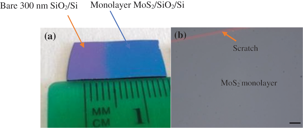
Figure 1: (a) Optical images of a centimeter scale MoS2 monolayer (right part) and the bare SiO2 covered Si substrate (the left purple part). (b): An optical image of scratched MoS2 monolayer, the scale bar is 5 μm
Following growth, we used a JEOL JSPM-5200 atomic force microscope to take direct thickness measurements. The film was first scratched with a sharp tip, and measurements were taken at the edges (across the red arrow) of the scratch, as shown in Fig. 2, with the corresponding height profile displayed in the inset. The distance between the substrate and the crystal edge is measured to be 0.8 nm. This value is consistent with the findings from mechanically exfoliated MoS2 monolayers reported in the literature [21].
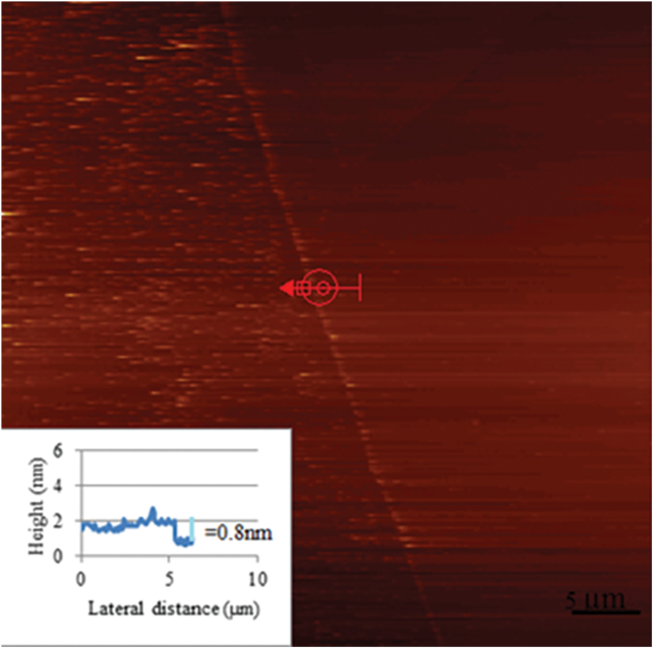
Figure 2: AFM image of MoS2 monolayer film, the measurements are taken along the red line with the inset showing thickness profile
Raman spectroscopy is one of the most widely used techniques in the field of transitional metal dichalcogenides TMDs for qualitative thickness measurements. Raman peaks are known as E12 g and A1 g modes, which correspond to the in-plane vibrations of Mo and S atoms and the out-of-plane vibrations of S atoms. The distance between these two peaks is highly dependent on the thickness of the MoS2 film [22]. As the thin film thickness decreases, so do the separation between the peaks, causing the E12 g peak to red-shift (phonon soften) and the A1 g peak to blue-shift (phonon stiffen), and such shifts in the Raman peaks can be used to determine the layer number of MoS2 [22]. In our case, Raman measurements were performed at room temperature under ambient conditions using a JY Horiba HR800 micro-Raman system. A 532 nm wavelength laser beam with a power of 0.5 mW and a spot diameter of 1 μm was focused on the sample. A typical Raman spectrum of a continuous film grown at 800°C is shown in Fig. 3. The E12 g peak is at 383.64 cm−1 and the A1 g peak is at 404.63 cm−1, with a separation of about 21 cm−1. These measurements are consistent with those reported for CVD-grown MoS2 monolayers [23].
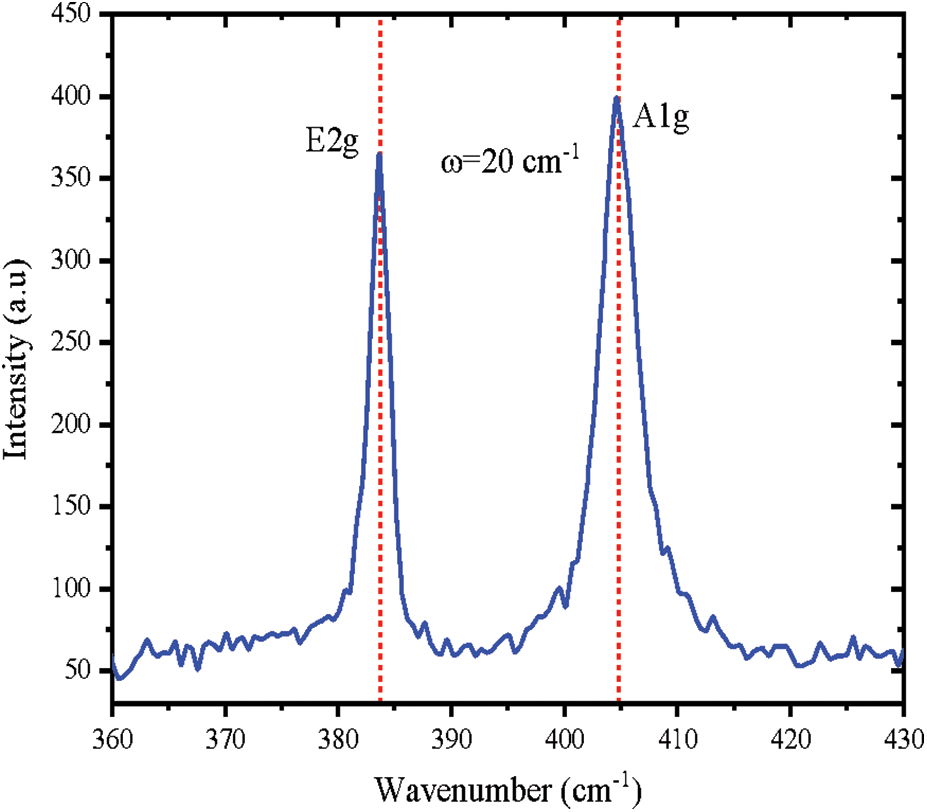
Figure 3: Raman spectrum of a continuous MoS2 monolayer film grown at 800°C
The optical properties of monolayer samples were studied using the same Raman system mentioned above. Fig. 4 shows a typical example of photoluminescence (PL) for the as-grown MoS2 monolayers. The A and B excitons, with centers at 1.80 and 1.96 eV, are associated with direct transitions from the lowest conduction band to the spin-orbit split valence bands. This result is consistent with PL measurements from mechanically exfoliated MoS2 monolayers [21]. A exciton has a full width at half maximum (FWHM) width of 70 meV. This result is comparable to mechanically exfoliated MoS2 monolayers, confirming our films’ high quality [24]. The PL spectra of single-layer MoS2 were fitted with three Lorentzian functions with the Trion peak centered at 1.8 eV and the neutral exciton peak at 1.82 eV [25]. The presence of the Trion peak in our films confirms the n-type doping of the MoS2 by charge transfer effects from the SiO2 substrate and this result is in good agreement with previous reports [26,27].

Figure 4: Lorentzian peak fitting of MoS2 monolayer PL spectra showing neutral exciton and trion peaks
Aberration-corrected transmission electron microscopy was used to assess the crystal quality of the monolayer films (TEM). Fig. 5a shows a MoS2 monolayer film transferred to a TEM grid using a poly (methyl methacrylate) (PMMA) assisted method (see materials and method for more details). The transferred film’s continuity indicated that the grown sample was of high quality; folds and holes observed on the TEM specimen were caused by the transfer process. An HRTEM image of the same monolayer region is shown in Fig. 5b. The corresponding selected area diffraction patterns (SAED) with the [001] zone axis are shown in Fig. 5c. The monolayer can be seen to have a high-quality single-crystalline nature with hexagonal lattice symmetry. We determined the value of the MoS2 monolayer lattice constant (a = 3.20) using SAED diffraction spots. This value is consistent with those reported in the literature [23,28].
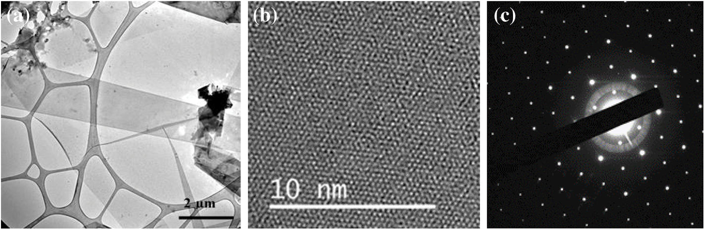
Figure 5: (a) Transferred MoS2 monolayer on lacey carbon film (b) HRTEM image of monolayer region (c) SAED from the same region in (b)
By transferring large-scale monolayer MoS2 (as mentioned in materials and method), we could fabricate MoS2/n-Si Schottky solar cell devices with MoS2 monolayer up to 1 cm2 area on the n-Si substrate. The solar cell fabrication process is summarized in Fig. 6.
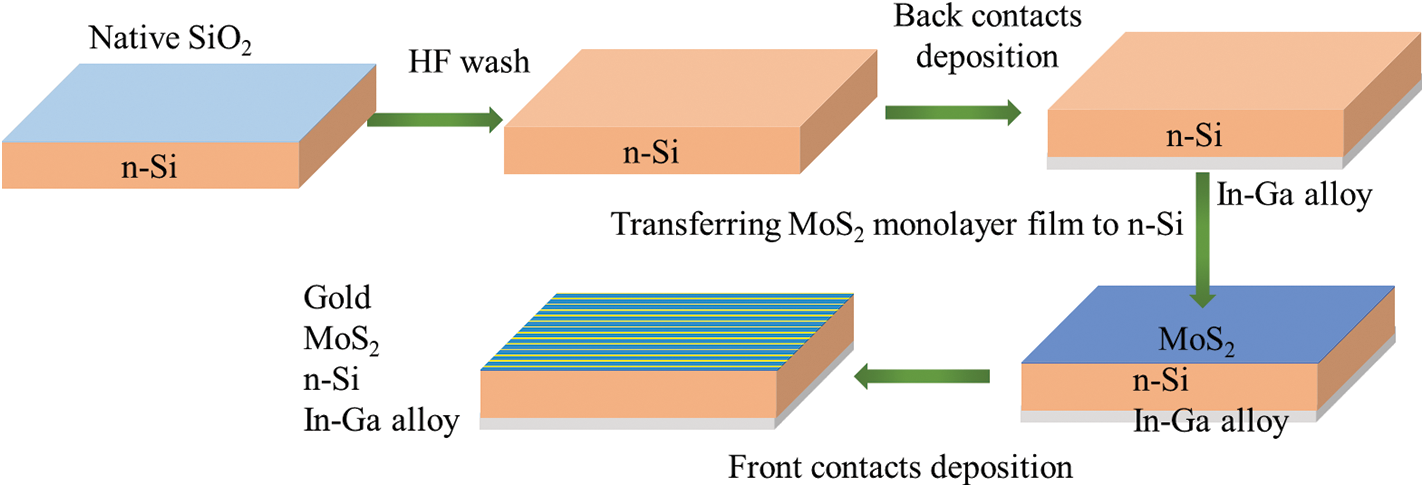
Figure 6: Fabrication procedure of monolayer MoS2/n-Si Schottky solar cell
The photovoltaic characteristics of the MoS2/n-Si Schottky solar can be explained by looking at the energy-band diagram of the MoS2/n-Si junction, which is shown in Fig. 7. When MoS2 monolayers are deposited on the surface of n-Si, electrons flow from n-Si into MoS2 at the interface due to the higher Si’s electron affinity [29]. When the Fermi levels of both materials are equal, the flowing process comes to an end, and the MoS2/n-Si Schottky solar cell is formed. The resultant band bending caused by electron flow results in the formation of a barrier for electron transport at the interface. Under illumination, the incident photons with energy larger than the bandgap of MoS2 monolayers (1.8 eV), the excitons from monolayer MoS2 and n-Si were generated. The built-in potential of about 201.29 mV at the interface of MoS2/n-Si is strong enough to separate the photo-generated electrons and holes and drift the electrons from MoS2 to n-Si and holes from n-Si to MoS2 monolayer [20].
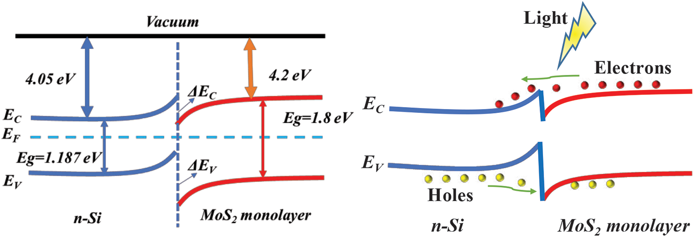
Figure 7: The band alignment at the interface between MoS2/n-Si at equilibrium (left). Electron-hole flow in the n-n homo-junction solar cell under illumination (right)
The I-V characteristics of a fabricated Schottky solar cell under dark and light illumination of 100 mW cm−2 are shown in Fig. 8. In the light, the current of the solar cell at a given voltage is greater than in the dark. This demonstrates that light absorption generates a photocurrent due to excitons produced in MoS2 and n-Si. According to the measurements, our device has an open circuit voltage of 0.32 V and a short circuit current of 14.8 mA cm−2. The fill factor and power conversion efficiency were calculated to be 53% and 2.46%, respectively.
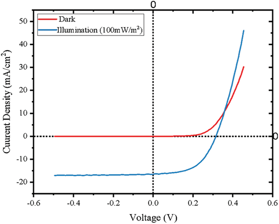
Figure 8: I-V characteristics of MoS2/n-Si Schottky solar cell under dank and illumination of 100 mW cm−2
The external quantum efficiency (EQE) of the monolayer MoS2/n-Si Schottky solar cell in the wavelength range of 300 nm–1100 nm is shown in Fig. 9. EQE of the constructed solar cell is identical to the silicon-based solar cells [30] As the Mos2 monolayer is semi-transparent and absorbs only up to 10% of the incident light thus, the generated carriers in the underlying n-Si layer are the main contributors to the photovoltaic current in the cell. The highest EQE (44%) recorded for our device is centered at 530 nm (2.34 eV).
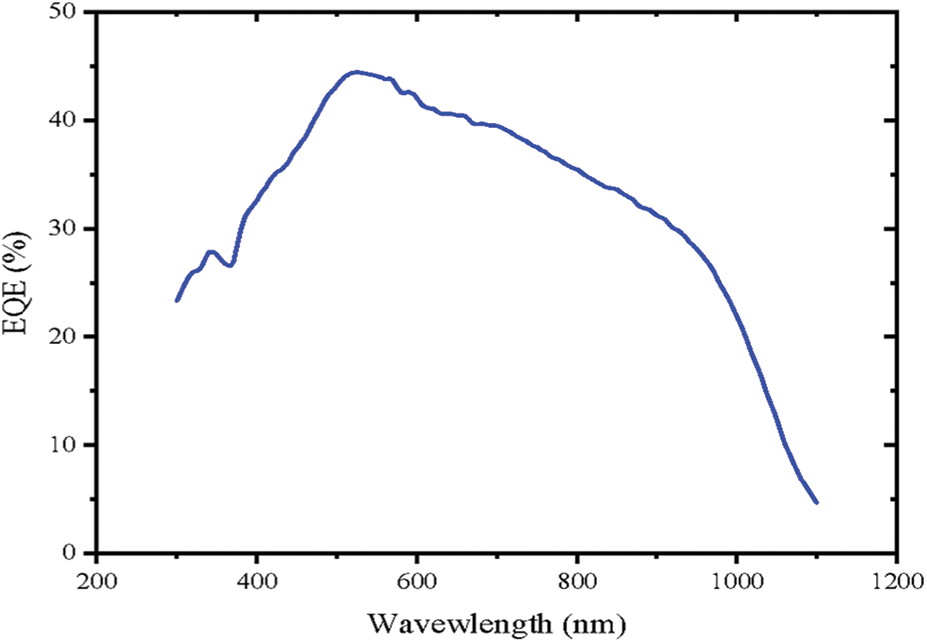
Figure 9: EQE spectra of MoS2/n-Si Schottky solar cell
Using a chemical vapor deposition technique, centimeter-scale MoS2 monolayer films were grown on a SiO2/Si substrate. The as-grown monolayer films are transferred to an n-Si silicon wafer to form the MoS2/n-Si Schottky solar cell. Under 100 mW cm−2 illumination, the Schottky solar cell has a large short circuit current density of 14.8 mA cm−2, an open circuit voltage of 0.32 V, a fill factor of 53%, and an efficiency of 2.46%. Photovoltaic characteristics were explained in terms of energy-band alignment mechanisms. Our findings show that MoS2/n-Si Schottky solar cells have a bright future in the field of solar cells.
Acknowledgement: The author extends his appreciation to Dr. Kun Huang from Silicon Laboratory at Zhejiang University and Prof. Dr. Jun Yuan from York University (UK) for help with constructing solar cells and measuring IV-Characteristics and quantum efficiency. This research was supported by the Kurdistan Regional Government, Human Capacity Development Program (HCDP).
Funding Statement: The author received no specific funding for this study.
Conflicts of Interest: The author declares that they have no conflicts of interest to report regarding the present study.
1. Butler, S. Z., Hollen, S. M., Cao, L., Cui, Y., Gupta, J. A. et al. (2013). Progress, challenges, and opportunities in two-dimensional materials beyond graphene. ACS Nano, 7(4), 2898–2926. DOI 10.1021/nn400280c. [Google Scholar] [CrossRef]
2. Miró, P., Audiffred, M., Heine, T. (2014). An atlas of two-dimensional materials. Chemical Society Reviews, 43(18), 6537–6554. DOI 10.1039/c4cs00102h. [Google Scholar] [CrossRef]
3. Chhowalla, M., Shin, H. S., Eda, G., Li, L. J., Loh, K. P. et al. (2013). The chemistry of two-dimensional layered transition metal dichalcogenide nanosheets. Nature Chemistry, 5(4), 263–275. DOI 10.1038/nchem.1589. [Google Scholar] [CrossRef]
4. Wilson, J. A., Yoffe, A. D. (1969). The transition metal dichalcogenides discussion and interpretation of the observed optical, electrical and structural properties. Advances in Physics, 18(73), 193–335. DOI 10.1080/00018736900101307. [Google Scholar] [CrossRef]
5. Mak, K. F., Lee, C., Hone, J., Shan, J., Heinz, T. F. (2010). Atomically thin MoS2: A new direct-gap semiconductor. Physical Review Letters, 105(13), 136805. DOI 10.1103/PhysRevLett.105.136805. [Google Scholar] [CrossRef]
6. Huo, N., Gupta, S., Konstantatos, G. (2017). Mos2-HgTe quantum Dot hybrid photodetectors beyond 2 μm. Advanced Materials, 29(17), 1606576. DOI 10.1002/adma.201606576. [Google Scholar] [CrossRef]
7. Radisavljevic, B., Radenovic, A., Brivio, J., Giacometti, V., Kis, A. (2011). Single-layer MoS2 transistors. Nature Nanotechnology, 6(3), 147–150. DOI 10.1038/nnano.2010.279. [Google Scholar] [CrossRef]
8. Bertolazzi, S., Brivio, J., Kis, A. (2011). Stretching and breaking of ultrathin MoS2. ACS Nano, 5(12), 9703–9709. DOI 10.1021/nn203879f. [Google Scholar] [CrossRef]
9. Furchi, M. M., Pospischil, A., Libisch, F., Burgdörfer, J., Mueller, T. (2014). Photovoltaic effect in an electrically tunable van der Waals heterojunction. Nano Letters, 14(8), 4785–4791. DOI 10.1021/nl501962c. [Google Scholar] [CrossRef]
10. Song, Y., Li, X., Mackin, C., Zhang, X., Fang, W. et al. (2015). Role of interfacial oxide in high-efficiency graphene-silicon schottky barrier solar cells. Nano Letters, 15(3), 2104–2110. DOI 10.1021/nl505011f. [Google Scholar] [CrossRef]
11. Li, X., Chen, W., Zhang, S., Wu, Z., Wang, P. et al. (2015). 18.5% efficient graphene/GaAs van der Waals heterostructure solar cell. Nano Energy, 16, 310–319. DOI 10.1016/j.nanoen.2015.07.003. [Google Scholar] [CrossRef]
12. Bernardi, M., Palummo, M., Grossman, J. C. (2013). Extraordinary sunlight absorption and one nanometer thick photovoltaics using two-dimensional monolayer materials. Nano Letters, 13(8), 3664–3670. DOI 10.1021/nl401544y. [Google Scholar] [CrossRef]
13. Tsai, M. L., Su, S. H., Chang, J. K., Tsai, D. S., Chen, C. H. et al. (2014). Monolayer MoS2 heterojunction solar cells. ACS Nano, 8(8), 8317–8322. DOI 10.1021/nn502776h. [Google Scholar] [CrossRef]
14. Zhao, Y., Ouyang, G. (2019). Thickness-dependent photoelectric properties of MoS2/Si heterostructure solar cells. Scientific Reports, 9(1), 17381. DOI 10.1038/s41598-019-53936-2. [Google Scholar] [CrossRef]
15. Lin, S., Li, X., Wang, P., Xu, Z., Zhang, S. et al. (2015). Interface designed MoS2/GaAs heterostructure solar cell with sandwich stacked hexagonal boron nitride. Scientific Reports, 5(1), 15103. DOI 10.1038/srep15103. [Google Scholar] [CrossRef]
16. Li, S. L., Zhang, L., Zhong, X., Gobbi, M., Bertolazzi, S. et al. (2019). Nano-subsidence-assisted precise integration of patterned Two-dimensional materials for high-performance photodetector arrays. ACS Nano, 13(2), 2654–2662. DOI 10.1021/acsnano.9b00889. [Google Scholar] [CrossRef]
17. Yoshikawa, K., Kawasaki, H., Yoshida, W., Irie, T., Konishi, K. et al. (2017). Silicon heterojunction solar cell with interdigitated back contacts for a photoconversion efficiency over 26%. Nature Energy, 2(5), 17032. DOI 10.1038/nenergy.2017.32. [Google Scholar] [CrossRef]
18. Shanmugam, M., Durcan, C. A., Yu, B. (2012). Layered semiconductor molybdenum disulfide nanomembrane based schottky-barrier solar cells. Nanoscale, 4(23), 7399–7405. DOI 10.1039/c2nr32394j. [Google Scholar] [CrossRef]
19. Nair, R. R., Blake, P., Grigorenko, A. N., Novoselov, K. S., Booth, T. J. et al. (2008). Fine structure constant defines visual transparency of graphene. Science, 320(5881), 1308. DOI 10.1126/science.1156965. [Google Scholar] [CrossRef]
20. Zhang, Y., Su, P., Liu, L., Qiu, P., Su, L. et al. (2020). The effect of MoS2 modulated doping with molybdenum-oxide on the photovoltaic performance for MoS2/n-Si heterojunction solar cells. Solar Energy, 208, 1048–1057. DOI 10.1016/j.solener.2020.08.062. [Google Scholar] [CrossRef]
21. Splendiani, A., Sun, L., Zhang, Y., Li, T., Kim, J. et al. (2010). Emerging photoluminescence in monolayer MoS2. Nano Letters, 10(4), 1271–1275. DOI 10.1021/nl903868w. [Google Scholar] [CrossRef]
22. Lee, C., Yan, H., Brus, L. E., Heinz, T. F., Hone, J. et al. (2010). Anomalous lattice vibrations of single-and few-layer MoS2. ACS Nano, 4(5), 2695–2700. DOI 10.1021/nn1003937. [Google Scholar] [CrossRef]
23. Yu, Y., Li, C., Liu, Y., Su, L., Zhang, Y. et al. (2013). Controlled scalable synthesis of uniform, high-quality monolayer, and few-layer MoS2 films. Scientific Reports, 3(1), 1866. DOI 10.1038/srep01866. [Google Scholar] [CrossRef]
24. Sercombe, D., Schwarz, S., Del Pozo-Zamudio, O., Liu, F., Robinson, B. J. et al. (2013). Optical investigation of the natural electron doping in thin MoS2 films deposited on dielectric substrates. Scientific Reports, 3(1), 3489. DOI 10.1038/srep03489. [Google Scholar] [CrossRef]
25. Li, Y., Qi, Z., Liu, M., Wang, Y., Cheng, X. et al. (2014). Photoluminescence of monolayer MoS2 on LaAlO3 and SrTiO3 substrates. Nanoscale, 6(24), 15248–15254. DOI 10.1039/c4nr04602a. [Google Scholar] [CrossRef]
26. Mak, K. F., He, K., Lee, C., Lee, G. H., Hone, J. et al. (2013). Tightly bound trions in monolayer MoS2. Nature Materials, 12(3), 207–211. DOI 10.1038/nmat3505. [Google Scholar] [CrossRef]
27. Scheuschner, N., Ochedowski, O., Kaulitz, A. M., Gillen, R., Schleberger, M. et al. (2014). Photoluminescence of freestanding single-and few-layer MoS2. Physical Review B, 89(12), 125406. DOI 10.1103/physrevb.89.125406. [Google Scholar] [CrossRef]
28. Huang, Y. L., Chen, Y., Zhang, W., Quek, S. Y., Chen, C. H. et al. (2015). Bandgap tunability at single-layer molybdenum disulfide grain boundaries. Nature Communications, 6(1), 6298. DOI 10.1038/ncomms7298. [Google Scholar] [CrossRef]
29. Ma, X. Y., Shi, M. Y. (2013). Study of the electrical contact properties of monolayer MoS2/Si heterojunction. Advanced Materials Research, 660, 57–60. DOI 10.4028/www.scientific.net/amr.660.57. [Google Scholar] [CrossRef]
30. Bae, S., Oh, W., Lee, K. D., Kim, S., Kim, H. et al. (2017). Potential induced degradation of n-type crystalline silicon solar cells with p+ front junction. Energy Science & Engineering, 5(1), 30–37. DOI 10.1002/ese3.146. [Google Scholar] [CrossRef]
 | This work is licensed under a Creative Commons Attribution 4.0 International License, which permits unrestricted use, distribution, and reproduction in any medium, provided the original work is properly cited. |